

Page 1
General Description
The MAX5080/MAX5081 are 250kHz PWM step-down
DC-DC converters with an on-chip, 0.3Ω high-side
switch. The input voltage range is 4.5V to 40V for the
MAX5080 and 7.5V to 40V for the MAX5081. The output
is adjustable from 1.23V to 32V and can deliver up to
1A of load current.
Both devices utilize a voltage-mode control scheme for
good noise immunity in the high-voltage switching environment and offer external compensation allowing for
maximum flexibility with a wide selection of inductor values and capacitor types. The switching frequency is
internally fixed at 250kHz and can be synchronized to
an external clock signal through the SYNC input. Light
load efficiency is improved by automatically switching
to a pulse-skip mode.
All devices include programmable undervoltage lockout and soft-start. Protection features include cycle-bycycle current limit, hiccup-mode output short-circuit
protection, and thermal shutdown. Both devices are
available in a space-saving, high-power (2.7W), 16-pin
TQFN package and are rated for operation over the
-40°C to +125°C temperature range.
Applications
FireWire®Power Supplies Automotive
Distributed Power Industrial
Features
♦ 4.5V to 40V (MAX5080) or 7.5V to 40V (MAX5081)
Input Voltage Range
♦ 1A Output Current
♦ V
OUT
Range From 1.23V to 32V
♦ Internal High-Side Switch
♦ Fixed 250kHz Internal Oscillator
♦ Automatic Switchover to Pulse-Skip Mode at
Light Loads
♦ External Frequency Synchronization
♦ Thermal Shutdown and Short-Circuit Protection
♦ Operates Over the -40°C to +125°C Temperature
Range
♦ Space-Saving (5mm x 5mm) High-Power 16-Pin
TQFN Package
MAX5080/MAX5081
1A, 40V, MAXPower Step-Down
DC-DC Converters
________________________________________________________________ Maxim Integrated Products 1
19-3656; Rev 0; 5/05
For pricing, delivery, and ordering information, please contact Maxim/Dallas Direct! at
1-888-629-4642, or visit Maxim’s website at www.maxim-ic.com.
Ordering Information
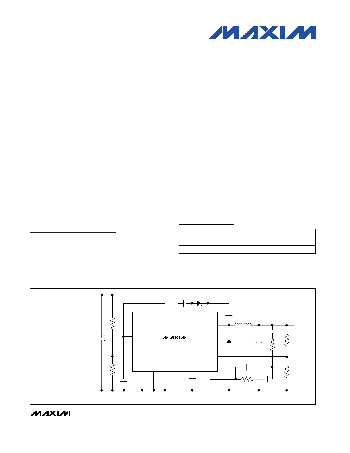
Typical Operating Circuits
FireWire is a registered trademark of Apple Computer, Inc.
Typical Operating Circuits continued at end of data sheet.
*EP = Exposed pad.
Pin Configurations appear at end of data sheet.
PART TEMP RANGE PIN-PACKAGE
MAX5080ATE -40°C to +125°C 16 TQFN-EP*
MAX5081ATE -40°C to +125°C 16 TQFN-EP*
V
IN
4.5V TO 40V
IN
R1
C1
R2
C2
PGND
REG
ON/OFF
SYNC SGND PGND SS COMP
DVREG
C-
MAX5080
D1
C
F
C
BST
C+
LX
FB
C
SS
BST
L1
C6
D2
C8
R5
C5
C7
R3
R6
R4
V
OUT
PGND
Page 2
MAX5080/MAX5081
1A, 40V, MAXPower Step-Down
DC-DC Converters
2 _______________________________________________________________________________________
ABSOLUTE MAXIMUM RATINGS
Stresses beyond those listed under “Absolute Maximum Ratings” may cause permanent damage to the device. These are stress ratings only, and functional
operation of the device at these or any other conditions beyond those indicated in the operational sections of the specifications is not implied. Exposure to
absolute maximum rating conditions for extended periods may affect device reliability.
IN, ON/OFF to SGND..............................................-0.3V to +45V
LX to SGND .................................................-0.3V to (V
IN
+ 0.3V)
BST to SGND ................................................-0.3V to (V
IN
+ 12V)
BST to LX................................................................-0.3V to +12V
PGND to SGND .....................................................-0.3V to +0.3V
REG, DVREG, SYNC to SGND ...............................-0.3V to +12V
FB, COMP, SS to SGND ...........................-0.3V to (V
REG
+ 0.3V)
C+ to PGND (MAX5080 only)................(V
DVREG
- 0.3V) to +12V
C- to PGND (MAX5080 only)................-0.3V to (V
DVREG
+ 0.3V)
Continuous current through internal power MOSFET (pins 11/12
connected together and pins 13/14 connected together)
T
J
= +125°C.........................................................................3A
T
J
= +150°C.........................................................................2A
Continuous Power Dissipation
*
(TA= +70°C)
16-Pin TQFN (derate 33.3mW/°C above +70°C) ...2666.7mW
16-Pin TQFN (θ
JA
)........................................................30°C/W
16-Pin TQFN (θ
JC
).......................................................1.7°C/W
Operating Temperature Range .........................-40°C to +125°C
Maximum Junction Temperature .....................................+150°C
Storage Temperature Range .............................-60°C to +150°C
Lead Temperature (soldering, 10s) .................................+300°C
ELECTRICAL CHARACTERISTICS
(VIN= V
ON/OFF
= 12V, V
REG
= V
DVREG
, V
SYNC
= PGND = SGND, TA= TJ= -40°C to +125°C, unless otherwise noted. Typical values
are at T
A
= + 25°C.) (Note 1)
*As per JEDEC 51 Standard
Input Voltage Range V
Undervoltage Lockout Threshold UVLO
Undervoltage Lockout Hysteresis UVLO
Switching Supply Current (PWM
Operation)
Efficiency
No-Load Supply Current
(PFM Operation)
Shutdown Current I
ON/OFF CONTROL
Input Voltage Threshold V
Input Voltage Hysteresis 0.12 V
Input Bias Current V
ERROR AMPLIFIER/SOFT-START
Soft-Start Current I
Reference Voltage (Soft-Start) V
FB Regulation Voltage V
FB Input Range 0 1.5 V
FB Input Current -250 +250 nA
COMP Voltage Range I
Open-Loop Gain 80 dB
Unity-Gain Bandwidth 1.8 MHz
PARAMETER SYMBOL CONDITIONS MIN TYP MAX UNITS
MAX5080 4.5 40
IN
MAX5081 7.5 40
VIN rising, MAX5080 3.9 4.2
rising, MAX5081 6.8 7.3
V
IN
MAX5080 0.4
HYST
MAX5081 0.7
I
SW
VFB = 0V, MAX5080 10.5
VFB = 0V, MAX5081 9.5
VIN = 12V, V
= 4.5V, V
V
IN
OUT
OUT
(MAX5080)
MAX5080 1.4 2.5
MAX5081 1.3 2.3
SS
FB
V
I
SHDN
ON/ OFFVON/ OFF
SS
= 0V, VIN = 40V 200 300 µA
ON/OFF
rising 1.20 1.23 1.25 V
= 0 to 40V -250 +250 nA
ON/OFF
= -500µA to +500µA 1.215 1.228 1.240 V
COMP
= -500µA to +500µA 0.25 4.50 V
COMP
= 3.3V, I
= 3.3V, I
= 1A 84
OUT
= 1A
OUT
88
81524µA
1.215 1.228 1.240 V
V
V
V
mA
%
mA
Page 3
MAX5080/MAX5081
1A, 40V, MAXPower Step-Down
DC-DC Converters
_______________________________________________________________________________________ 3
ELECTRICAL CHARACTERISTICS (continued)
(VIN= V
ON/OFF
= 12V, V
REG
= V
DVREG
, V
SYNC
= PGND = SGND, TA= TJ= -40°C to +125°C, unless otherwise noted. Typical values
are at T
A
= + 25°C.) (Note 1)
FB Offset Voltage I
OSCILLATOR
Frequency f
Maximum Duty Cycle D
SYNC High-Level Voltage 2.2 V
SYNC Low-Level Voltage 0.8 V
SYNC Frequency Range f
PWM Modulator Gain f
Ramp Level Shift (Valley) 0.3 V
POWER SWITCH
Switch On-Resistance V
Switch Gate Charge V
Switch Leakage Current VIN = 40V, VLX = V
BST Leakage Current V
CHARGE PUMP
C- Output Voltage Low MAX5080 only, sinking 10mA 0.1 V
C- Output Voltage High
DVREG to C+ On-Resistance MAX5080 only, sourcing 10mA 10 Ω
LX to PGND On-Resistance Sinking 10mA 12 Ω
CURRENT-LIMIT COMPARATOR
Pulse-Skip Threshold I
Cycle-by-Cycle Current Limit I
Number of Consecutive ILIM
Events to Hiccup
Hiccup Timeout 512
INTERNAL VOLTAGE REGULATOR
Output Voltage V
Line Regulation
Load Regulation I
Dropout Voltage
PARAMETER SYMBOL CONDITIONS MIN TYP MAX UNITS
SYNC
= -500µA to +500µA -5 +5 mV
COMP
V
SW
MAX
PFM
ILIM
REG
= 0V 225 250 275 kHz
SYNC
V
= 0V, V
SYNC
V
= 0V, VIN = 7.5V, MAX5081 87
SYNC
V
= 0V, VIN ≤ 40V 87
SYNC
= 150kHz to 350kHz 10 V/V
SYNC
- V
BST
LX
- VLX = 6V 6 nC
BST
= VLX = VIN = 40V 10 µA
BST
MAX5080 only, relative to DVREG, sourcing
10mA
MAX5080 4.75 5 5.25
MAX5081 7.6 8 8.4
VIN = 5.5V to 40V, MAX5080 1
V
= 9.0V to 40V, MAX5081 1
IN
= 0 to 20mA 0.25 V
REG
VIN = 4.5V, I
= 7.5V, I
V
IN
= 4.5V, MAX5080 87
IN
150 350 kHz
= 6V 0.3 0.6 Ω
= 0V 10 µA
BST
0.1 V
100 200 300 mA
1.4 2 2.6 A
7
= 20mA, MAX5080 0.5
REG
= 20mA, MAX5081 0.5
REG
periods
%
Clock
V
mV/V
V
Page 4
MAX5080/MAX5081
1A, 40V, MAXPower Step-Down
DC-DC Converters
4 _______________________________________________________________________________________
ELECTRICAL CHARACTERISTICS (continued)
(VIN= V
ON/OFF
= 12V, V
REG
= V
DVREG
, V
SYNC
= PGND = SGND, TA= TJ= -40°C to +125°C, unless otherwise noted. Typical values
are at T
A
= + 25°C.) (Note 1)
Note 1: 100% production tested at TA= +25°C and TA= TJ= +125°C. Limits at -40°C are guaranteed by design.
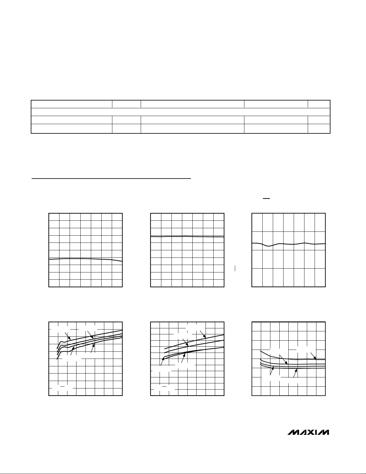
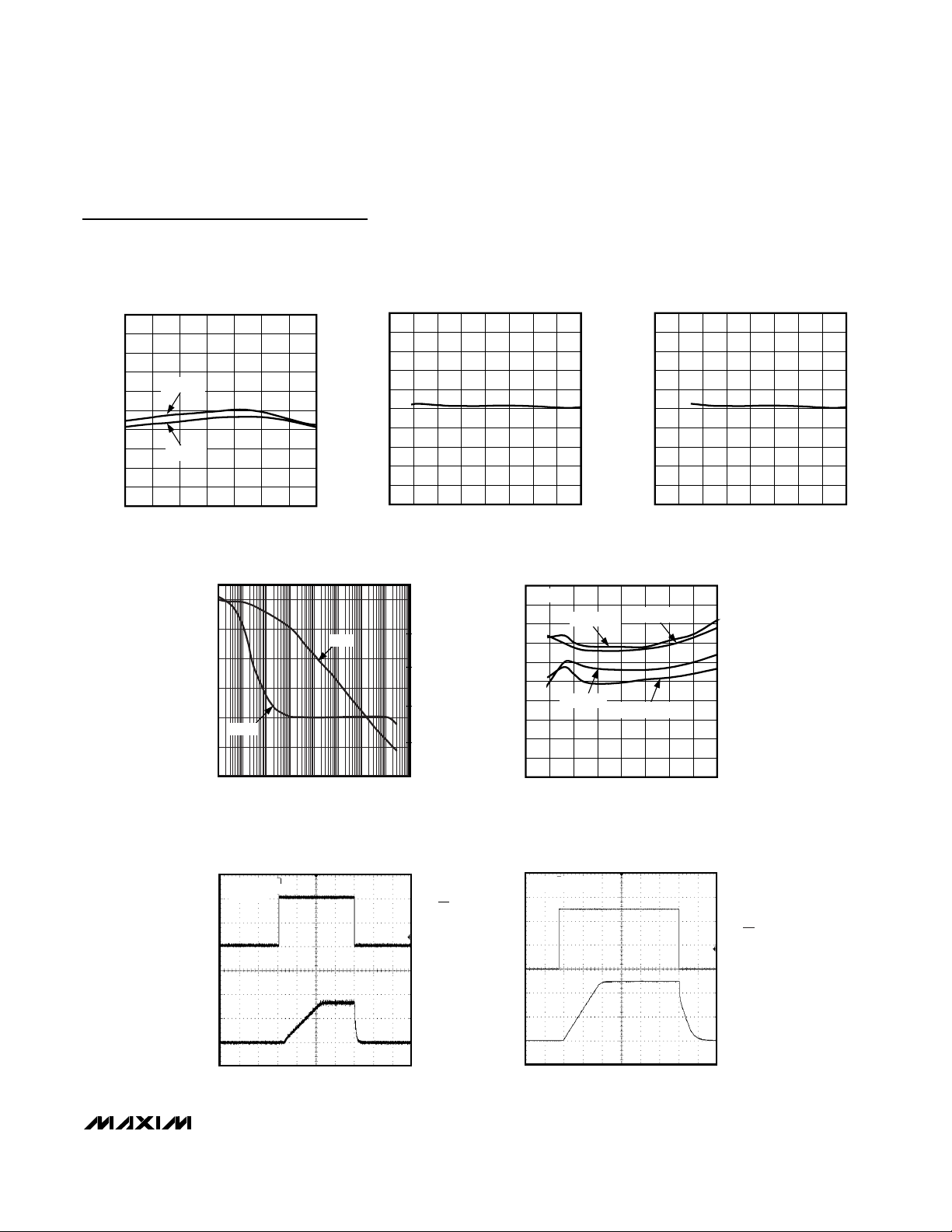
Typical Operating Characteristics
(VIN= 12V, see Figure 5 (MAX5080) and Figure 6 (MAX5081), TA= +25°C, unless otherwise noted.)
UNDERVOLTAGE LOCKOUT HYSTERESIS
vs. TEMPERATURE (MAX5080)
MAX5080 toc01
TEMPERATURE (°C)
UNDERVOLTAGE LOCKOUT HYSTERESIS (V)
1108535 6010-15
0.1
0.2
0.3
0.4
0.5
0.6
0.7
0.8
0.9
1.0
0
-40 135
UNDERVOLTAGE LOCKOUT HYSTERESIS
vs. TEMPERATURE (MAX5081)
MAX5080 toc02
TEMPERATURE (°C)
UNDERVOLTAGE LOCKOUT HYSTERESIS (V)
1108535 6010-15
0.1
0.2
0.3
0.4
0.5
0.6
0.7
0.8
0.9
1.0
0
-40 135
ON/OFF THRESHOLD HYSTERESIS
vs. TEMPERATURE
MAX5080 toc03
TEMPERATURE (°C )
ON/OFF THRESHOLD HYSTERESIS (V)
11085603510-15
0.05
0.10
0.15
0.20
0
-40 135
SHUTDOWN SUPPLY CURRENT
vs. INPUT VOLTAGE (MAX5080)
MAX5080 toc04
INPUT VOLTAGE (V)
SHUTDOWN SUPPLY CURRENT (µA)
353020 2510 155
25
50
75
100
125
150
175
200
225
250
0
040
TA = +135°C
TA = +25°C
TA = +85°C
TA = -40°C
V
ON/OFF
= 0V
SHUTDOWN SUPPLY CURRENT
vs. INPUT VOLTAGE (MAX5081)
MAX5080 toc05
INPUT VOLTAGE (V)
SHUTDOWN SUPPLY CURRENT (µA)
353020 2510 155
25
50
75
100
125
150
175
200
225
250
275
300
0
040
TA = +135°C
TA = +25°C
TA = +85°C
TA = -40°C
V
ON/OFF
= 0V
NO-LOAD SUPPLY CURRENT
vs. INPUT VOLTAGE (MAX5080)
MAX5080 toc06
INPUT VOLTAGE (V)
SUPPLY CURRENT (mA)
35305 10 15 20 25
0.5
1.0
1.5
2.0
2.5
3.0
3.5
4.0
0
040
TA = +135°C
TA = +25°C
TA = +85°C
TA = -40°C
THERMAL SHUTDOWN
Thermal Shutdown Temperature Temperature rising +160 °C
Thermal Shutdown Hysteresis 20 °C
PARAMETER SYMBOL CONDITIONS MIN TYP MAX UNITS
Page 5
OPERATING FREQUENCY
vs. TEMPERATURE
MAX5080 toc07
TEMPERATURE (°C)
OPERATING FREQUENCY (kHz)
1108535 6010-15
242
244
246
248
250
252
254
256
258
260
240
-40 135
VIN = 4.5V
VIN = 40V
MAXIMUM DUTY CYCLE
vs. INPUT VOLTAGE (MAX5080)
MAX5080 toc08
INPUT VOLTAGE (V)
MAXIMUM DUTY CYCLE (%)
353020 2510 155
82
84
86
88
90
92
94
96
98
100
80
040
MAXIMUM DUTY CYCLE
vs. INPUT VOLTAGE (MAX5081)
MAX5080 toc09
INPUT VOLTAGE (V)
MAXIMUM DUTY CYCLE (%)
353020 2510 155
82
84
86
88
90
92
94
96
98
100
80
040
MAX5080/MAX5081
1A, 40V, MAXPower Step-Down
DC-DC Converters
_______________________________________________________________________________________ 5
Typical Operating Characteristics (continued)
(VIN= 12V, see Figure 5 (MAX5080) and Figure 6 (MAX5081), TA= +25°C, unless otherwise noted.)
OPEN-LOOP GAIN/PHASE vs. FREQUENCY
MAX5080 toc10
FREQUENCY (kHz)
GAIN (dB)
PHASE (DEGREES)
10001001010.10.010.001
0
20
40
60
80
100
-20
75
100
125
150
175
50
0 10,000
GAIN
PHASE
OUTPUT CURRENT LIMIT
vs. INPUT VOLTAGE
MAX5080 toc11
INPUT VOLTAGE (V)
OUTPUT CURRENT LIMIT (A)
353020 2510 155
1.6
1.7
1.8
1.9
2.0
2.1
2.2
2.3
2.4
2.5
1.5
040
MAX5080
TA = +135°C
TA = +25°C
TA = +85°C
TA = -40°C
TURN-ON/OFF WAVEFORM
MAX5080 toc12
I
LOAD
= 1A
V
OUT
2V/div
V
ON/OFF
2V/div
2ms/div
TURN-ON/OFF WAVEFORM
MAX5080 toc13
V
ON/OFF
2V/div
V
OUT
2V/div
2ms/div
I
LOAD
= 100mA
Page 6
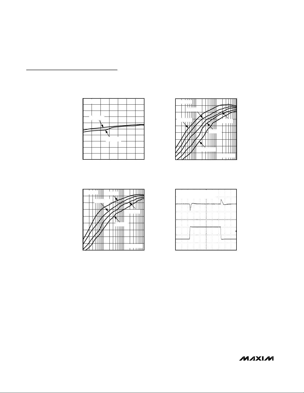
Typical Operating Characteristics (continued)
(VIN= 12V, see Figure 5 (MAX5080) and Figure 6 (MAX5081), TA= +25°C, unless otherwise noted.)
MAX5080/MAX5081
1A, 40V, MAXPower Step-Down
DC-DC Converters
6 _______________________________________________________________________________________
OUTPUT VOLTAGE vs. TEMPERATURE
3.40
MAX5080
3.38
3.36
3.34
3.32
3.30
3.28
OUTPUT VOLTAGE (V)
3.26
3.24
3.22
3.20
I
= 0A
LOAD
I
= 1A
LOAD
-40 135
TEMPERATURE (°C)
EFFICIENCY vs. LOAD CURRENT
100
V
= 5V
OUT
90
80
70
60
50
EFFICIENCY (%)
40
30
20
0
0.001 1
VIN = 7.5V
VIN = 12V
LOAD CURRENT (A)
VIN = 40V
0.10.01
1108535 6010-15
VIN = 24V
MAX5081
MAX5080 toc14
MAX5080 toc16
EFFICIENCY vs. LOAD CURRENT
100
V
= 3.3V
OUT
90
80
70
60
50
EFFICIENCY (%)
40
30
20
0
0.001 1
VIN = 7.5V
VIN = 4.5V
VIN = 24V
VIN = 40V
0.10.01
LOAD CURRENT (A)
LOAD-TRANSIENT RESPONSE
0
VIN = 12V, I
MAX5080
= 0.25A TO 1A
OUT
200µs/div
VIN = 12V
MAX5080
MAX5080 toc17
MAX5080 toc15
V
OUT
AC-COUPLED
200mV/div
I
LOAD
500mA/div
Page 7

MAX5080/MAX5081
1A, 40V, MAXPower Step-Down
DC-DC Converters
_______________________________________________________________________________________ 7
Typical Operating Characteristics (continued)
(VIN= 12V, see Figure 5 (MAX5080) and Figure 6 (MAX5081), TA= +25°C, unless otherwise noted.)
LX VOLTAGE AND INDUCTOR CURRENT
MAX5080 toc19
V
LX
5V/div
INDUCTOR CURRENT
200mA/div
2µs/div
I
LOAD
= 40mA
LX VOLTAGE AND INDUCTOR CURRENT
MAX5080 toc20
V
LX
5V/div
INDUCTOR CURRENT
100mA/div
2µs/div
I
LOAD
= 140mA
0
LX VOLTAGE AND INDUCTOR CURRENT
MAX5080 toc21
V
LX
5V/div
INDUCTOR CURRENT
500mA/div
2µs/div
I
LOAD
= 1A
0
LOAD-TRANSIENT RESPONSE
MAX5080 toc18
VIN = 4.5V, I
OUT
= 0.25A TO 1A
MAX5080
V
OUT
AC-COUPLED
500mV/div
I
LOAD
500mA/div
200µs/div
0
Page 8

MAX5080/MAX5081
1A, 40V, MAXPower Step-Down
DC-DC Converters
8 _______________________________________________________________________________________
Detailed Description
The MAX5080/MAX5081 are voltage-mode buck converters with internal 0.3Ω power MOSFET switches. The
MAX5080 has a wide input voltage range of 4.5V to
40V. The MAX5081’s input voltage range is 7.5V to 40V.
The internal low R
DS_ON
switch allows for up to 1A of
output current. The 250kHz fixed switching frequency,
external compensation, and voltage feed-forward simplify loop compensation design and allow for a variety
of L and C filter components. Both devices offer an
automatic switchover to pulse-skipping (PFM) mode,
providing low quiescent current and high efficiency at
light loads. Under no load, a PFM mode operation
reduces the current consumption to only 1.4mA. In
shutdown, the supply current falls to 200µA. Additional
features include an externally programmable undervoltage lockout through the ON/OFF pin, a programmable
soft-start, cycle-by-cycle current limit, hiccup mode
output short-circuit protection, and thermal shutdown.
PIN
MAX5080
FUNCTION
11
Error Amplifier Output. Connect COMP to the compensation feedback network.
22FB
Feedback Regulation Point. Connect to the center tap of a resistive divider from converter
output to SGND to set the output voltage. The FB voltage regulates to the voltage present at SS
(1.23V).
33
ON/OFF and External UVLO Control. The ON/OFF rising threshold is set to approximately 1.23V.
Connect to the center tap of a resistive divider from IN to SGND to set the UVLO (rising)
threshold. Pull ON/OFF to SGND to shut down the device. ON/OFF can be used for powersupply sequencing. Connect to IN for always-on operation.
44SS
Soft-Start and Reference Output. Connect a capacitor from SS to SGND to set the soft-start
time. See the Applications Information section to calculate the value of the CSS capacitor.
55
Oscillator Synchronization Input. SYNC can be driven by an external 150kHz to 350kHz clock to
synchronize the MAX5080/MAX5081’s switching frequency. Connect SYNC to SGND when not
used.
66
Gate Drive Supply for High-Side MOSFET Driver. Connect externally to REG for MAX5080.
Connect to REG and the anode of the boost diode for MAX5081.
7 — C+ Charge-Pump Flying Capacitor Positive Connection
8 — C- Charge-Pump Flying Capacitor Negative Connection
— 7, 8 N.C. No Connection. Not internally connected. Can be left floating or connected to SGND.
99
Power Ground Connection. Connect the input filter capacitor’s negative terminal, the anode of
the freewheeling diode, and the output filter capacitor’s return to PGND. Connect externally to
SGND at a single point near the input capacitor’s return terminal.
10 10 BST
High-Side Gate Driver Supply. Connect BST to the cathode of the boost diode and to the
positive terminal of the boost capacitor.
11, 12 11, 12 LX
Source Connection of Internal High-Side Switch. Connect the inductor and rectifier diode’s
anode to LX.
13, 14 13, 14 IN
Supply Input Connection. Connect to an external voltage source from 4.5V to 40V (MAX5080) or
a 7.5V to 40V (MAX5081).
15 15 REG
Internal Regulator Output. 5V output for the MAX5080 and 8V output for the MAX5081. Bypass
to SGND with at least a 1µF ceramic capacitor.
16 16
Signal Ground Connection. Solder the exposed pad to a large SGND plane. Connect SGND
and PGND together at one point near the input bypass capacitor return terminal.
EP EP EP Exposed Pad. Connect exposed pad to SGND.
Pin Description
MAX5081
NAME
COMP
ON/OFF
SYNC
DVREG
PGND
SGND
Page 9

MAX5080/MAX5081
1A, 40V, MAXPower Step-Down
DC-DC Converters
_______________________________________________________________________________________ 9
Internal Linear Regulator (REG)
REG is the output terminal of a 5V (MAX5080), or 8V
(MAX5081) LDO which is powered from IN and provides power to the IC. Connect REG externally to
DVREG to provide power for the high-side MOSFET
gate driver. Bypass REG to SGND with a ceramic
capacitor of at least 1µF. Place the capacitor physically
close to the MAX5080/MAX5081 to provide good
bypassing. During normal operation, REG is intended
for powering up only the internal circuitry and should
not be used to supply power to external loads.
Internal UVLO/External UVLO
The MAX5080/MAX5081 provides two undervoltage
lockouts (UVLOs). An internal UVLO looks at the input
voltage (VIN) and is fixed at 4.1V (MAX5080) or 7.1V
(MAX5081). An external UVLO is sensed and programmed at the ON/OFF pin. The external UVLO over-
rides the internal UVLO when the external UVLO is
higher than the internal UVLO. During startup, before
any operation begins, the input voltage and the voltage
at ON/OFF must exceed their respective UVLOs. The
external UVLO has a rising threshold of 1.23V with
0.12V of hysteresis. Program the external UVLO by
connecting a resistive divider from IN to ON/OFF to
SGND. Connect ON/OFF to IN directly to disable the
external UVLO.
Driving ON/OFF to ground places the MAX5080/
MAX5081 in shutdown. When in shutdown the internal
power MOSFET turns off, all internal circuitry shuts
down and the quiescent supply current reduces to
200µA. Connect an RC network from ON/OFF to SGND
to set a turn-on delay that can be used to sequence the
output voltages of multiple devices.
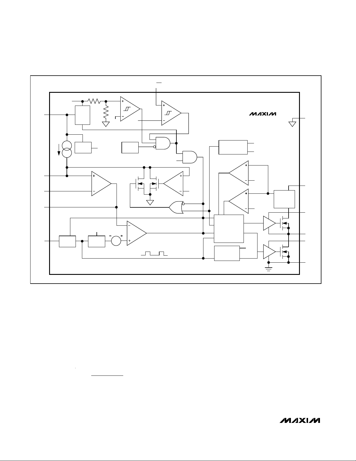
Figure 1. MAX5080 Simplified Block Diagram
REG
COMP
SYNC
ILIM
CLK
DVREGC+
MAX5080
DVREG
HIGH-SIDE
CURRENT
SENSE
SGND
IN
BST
LX
PGND
DVREG
OVERL
CHARGE-PUMP
MANAGEMENT
C-
LEVEL
SHIFT
OVERLOAD
MANAGEMENT
ILIM
PFM
LOGIC
REF_ILIM
REF_PFM
PCLK
SCLK
ON/OFF
IN
CLK
>1.23V ON
<1.11V OFF
REGOK
SSA
V
PCLK
EN
REF
LDO
EN
OSC
1.23V
EN
REF
RAMP
I
SS
SS
FB
1.23V
V
REF
E/A
IN
0.3V
1.23V
THERMAL
SHDN
CPWM
Page 10
MAX5080/MAX5081
1A, 40V, MAXPower Step-Down
DC-DC Converters
10 ______________________________________________________________________________________
Soft-Start and Reference (SS)
SS is the 1.23V reference bypass connection for the
MAX5080/MAX5081 and also controls the soft-start
period. At startup, after VINis applied and the internal
and external UVLO thresholds are reached, the device
enters soft-start. During soft-start, 15µA is sourced into
the capacitor (CSS) connected from SS to SGND causing the reference voltage to ramp up slowly. When V
SS
reaches 1.23V the output becomes fully active. Set the
soft-start time (tSS) using following equation:
where tSSis in seconds and CSSis in Farads.
Internal Charge Pump (MAX5080)
The MAX5080 features an internal charge pump to
enhance the turn-on of the internal MOSFET, allowing
for operation with input voltages down to 4.5V. Connect
a flying capacitor (CF) between C+ and C-, a boost
diode from C+ to BST, as well as a bootstrap capacitor
(C
BST
) between BST and LX to provide the gate drive
voltage for the high-side n-channel DMOS switch.
During the on-time, the flying capacitor is charged to
V
DVREG
. During the off-time, the positive terminal of the
flying capacitor (C+) is pumped to two times V
DVREG
and charge is dumped onto C
BST
to provide twice the
regulator voltage across the high-side DMOS driver.
Use a ceramic capacitor of at least 0.1µF for C
BST
and
CFlocated as close to the device as possible.
t
VC
A
SS
SS
=
×12315.
µ
Figure 2. MAX5081 Simplified Block Diagram
ON/OFF
IN
REG
LDO
EN
1.23V
1.23V
>1.23V ON
<1.11V OFF
MAX5081
SGND
I
SS
SS
FB
REF
1.23V
E/A
V
REF
THERMAL
SHDN
COMP
IN
SYNC
OSC
EN
RAMP
CPWM
0.3V
CLK
REGOK
SSA
REF_ILIM
REF_PFM
PCLK
SCLK
ILIM
CLK
HIGH-SIDE
CURRENT
SENSE
IN
BST
LX
DVREG
PGND
OVERL
OVERLOAD
ILIM
MANAGEMENT
ILIM
PFM
LOGIC
BOOTSTRAP
CONTROL
EN
V
REF
Page 11

MAX5080/MAX5081
1A, 40V, MAXPower Step-Down
DC-DC Converters
______________________________________________________________________________________ 11
For applications that do not require a 4.5V minimum
input, use the MAX5081. In this device the charge
pump is omitted and the input voltage range is from
7.5V to 40V. In this situation the boost diode and the
boost capacitor are still required (see the MAX5081
Typical Operating Circuit).
Gate Drive Supply (DVREG)
DVREG is the supply input for the internal high-side
MOSFET driver. The power for DVREG is derived from
the output of the internal regulator (REG). Connect
DVREG to REG externally. We recommend the use of
an RC filter (1Ω and 0.47µF) from REG to DVREG to filter the noise generated by the switching of the charge
pump. In the MAX5080, the high-side drive supply is
generated using the internal charge pump along with
the bootstrap diode and capacitor. In the MAX5081, the
high-side MOSFET driver supply is generated using
only the bootstrap diode and capacitor.
Error Amplifier
The output of the internal error amplifier (COMP) is available for frequency compensation (see the Compensation
Design section). The inverting input is FB, the noninverting input SS, and the output COMP. The error amplifier
has an 80dB open-loop gain and a 1.8MHz GBW product. See the Typical Operating Character-istics for the
Gain and Phase vs. Frequency graph.
Oscillator/Synchronization Input (SYNC)
With SYNC tied to SGND, the MAX5080/MAX5081 use
their internal oscillator and switch at a fixed frequency
of 250kHz. For external synchronization, drive SYNC
with an external clock from 150kHz to 350kHz. When
driven with an external clock, the device synchronizes
to the rising edge of SYNC.
PWM Comparator/Voltage Feedforward
An internal 250kHz ramp generator is compared
against the output of the error amplifier to generate the
PWM signal. The maximum amplitude of the ramp
(V
RAMP
) automatically adjusts to compensate for input
voltage and oscillator frequency changes. This causes
the VIN/V
RAMP
to be a constant 10V/V across the input
voltage range of 4.5V to 40V (MAX5080) or 7.5V to 40V
(MAX5081) and the SYNC frequency range of 150kHz
to 350kHz.
Output Short-Circuit Protection
(Hiccup Mode)
The MAX5080/MAX5081 protects against an output short
circuit by utilizing hiccup-mode protection. In hiccup
mode, a series of sequential cycle-by-cycle current-limit
events will cause the part to shut down and restart with
a soft-start sequence. This allows the device to operate
with a continuous output short circuit.
During normal operation, the current is monitored at the
drain of the internal power MOSFET. When the current
limit is exceeded, the internal power MOSFET turns off
until the next on-cycle and a counter increments. If the
counter counts seven consecutive current-limit events,
the device discharges the soft-start capacitor and
shuts down for 512 clock periods before restarting with
a soft-start sequence. Each time the power MOSFET
turns on and the device does not exceed the current
limit, the counter is reset.
Thermal-Overload Protection
The MAX5080/MAX5081 feature an integrated thermaloverload protection. Thermal-overload protection limits
the total power dissipation in the device and protects it
in the event of an extended thermal fault condition.
When the die temperature exceeds +160°C, an internal
thermal sensor shuts down the part, turning off the
power MOSFET and allowing the IC to cool. After the
temperature falls by 20°C, the part will restart with a
soft-start sequence.
Applications Information
Setting the Undervoltage Lockout
When the voltage at ON/OFF rises above 1.23V, the
MAX5080/MAX5081 turns on. Connect a resistive
divider from IN to ON/OFF to SGND to set the UVLO
threshold (see Figure 5). First select the ON/OFF to the
SGND resistor (R2) then calculate the resistor from IN
to ON/OFF (R1) using the following equation:
where VINis the input voltage at which the converter
turns on, V
ON/OFF
= 1.23V and R2 is chosen to be less
than 600kΩ.
If the external UVLO divider is not used, connect
ON/OFF to IN directly. In this case, an internal undervoltage lockout feature monitors the supply voltage at
IN and allows operation to start when IN rises above
4.1V (MAX5080) and 7.1V (MAX5081).
Setting the Output Voltage
Connect a resistive divider from OUT to FB to SGND to
set the output voltage. First calculate the resistor from
OUT to FB using the guidelines in the Compensation
Design section. Once R3 is known, calculate R4 using
the following equation:
RR
12 1=×
⎡
⎢
V
⎢
ON/OFF
⎣
V
IN
⎤
−
⎥
⎥
⎦
Page 12

MAX5080/MAX5081
1A, 40V, MAXPower Step-Down
DC-DC Converters
12 ______________________________________________________________________________________
where VFB= 1.23V.
Inductor Selection
Three key inductor parameters must be specified for
operation with the MAX5080/MAX5081: inductance
value (L), peak inductor current (I
PEAK
), and inductor
saturation current (I
SAT
). The minimum required inductance is a function of operating frequency, input-to-output voltage differential, and the peak-to-peak inductor
current (∆I
P-P
). Higher ∆I
P-P
allows for a lower inductor
value while a lower ∆I
P-P
requires a higher inductor
value. A lower inductor value minimizes size and cost
and improves large-signal and transient response, but
reduces efficiency due to higher peak currents and
higher peak-to-peak output voltage ripple for the same
output capacitor. On the other hand, higher inductance
increases efficiency by reducing the ripple current.
Resistive losses due to extra wire turns can exceed the
benefit gained from lower ripple current levels especially when the inductance is increased without also allowing for larger inductor dimensions. A good compromise
is to choose ∆I
P-P
equal to 40% of the full load current.
Calculate the inductor using the following equation:
VINand V
OUT
are typical values so that efficiency is optimum for typical conditions. The switching frequency (fSW)
is fixed at 250kHz or can vary between 150kHz and
350kHz when synchronized to an external clock (see the
Oscillator/Synchronization Input (SYNC) section). The
peak-to-peak inductor current, which reflects the peak-topeak output ripple, is worst at the maximum input voltage.
See the Output Capacitor Selection section to verify that
the worst-case output ripple is acceptable. The inductor
saturating current (I
SAT
) is also important to avoid runaway current during continuous output short circuit.
Select an inductor with an I
SAT
specification higher than
the maximum peak current limit of 2.6A.
Input Capacitor Selection
The discontinuous input current of the buck converter
causes large input ripple currents and therefore the
input capacitor must be carefully chosen to keep the
input voltage ripple within design requirements. The
input voltage ripple is comprised of ∆VQ(caused by the
capacitor discharge) and ∆V
ESR
(caused by the ESR of
the input capacitor). The total voltage ripple is the sum
of ∆V
Q
and ∆V
ESR
. Calculate the input capacitance and
ESR required for a specified ripple using the following
equations:
where
I
OUT_MAX
is the maximum output current, D is the duty
cycle, and fSWis the switching frequency.
The MAX5080/MAX5081 includes internal and external
UVLO hysteresis and soft-start to avoid possible unintentional chattering during turn-on. However, use a bulk
capacitor if the input source impedance is high. Use
enough input capacitance at lower input voltages to
avoid possible undershoot below the undervoltage
lockout threshold during transient loading.
Output Capacitor Selection
The allowable output voltage ripple and the maximum
deviation of the output voltage during load steps determine the output capacitance and its ESR. The output
ripple is mainly composed of ∆VQ(caused by the
capacitor discharge) and ∆V
ESR
(caused by the voltage drop across the equivalent series resistance of the
output capacitor). The equations for calculating the
peak-to-peak output voltage ripple are:
Normally, a good approximation of the output voltage
ripple is ∆V
RIPPLE
≈∆V
ESR
+ ∆VQ. If using ceramic
capacitors, assume the contribution to the output voltage ripple from ESR and the capacitor discharge to be
R
R
4
=
OUT IN OUT
Lf=
VI
IN SW P-P
3
⎡
V
OUT
⎢
V
⎣
FB
⎤
−
1
⎥
⎦
()
−VVV
××
∆
∆
V
ESR
=
⎛
I
⎜
OUT_MAX
⎝
IDD
OUT_MAX
=
C
IN
()
VV V
∆I
P-P
IN OUT OUT
=
D
ESR
I
∆
⎞
P-P
+
×
∆
f
×
V
QSW
−
VL
××
f
IN SW
V
OUT
=
V
IN
⎟
⎠
2
−
1
()
×
and
∆
I
∆
V
=
Q
1
6C f
PP
××
OUT SW
∆∆
VI
=×
ESR
ESR P-P
Page 13

MAX5080/MAX5081
1A, 40V, MAXPower Step-Down
DC-DC Converters
______________________________________________________________________________________ 13
equal to 20% and 80%, respectively. ∆I
P-P
is the peak-topeak inductor current (see the Input Capacitors Selection
section) and fSWis the converter’s switching frequency.
The allowable deviation of the output voltage during
fast load transients also determines the output capacitance, its ESR, and its equivalent series inductance
(ESL). The output capacitor supplies the load current
during a load step until the controller responds with a
greater duty cycle. The response time (t
RESPONSE
)
depends on the closed-loop bandwidth of the converter
(see the Compensation Design section). The resistive
drop across the output capacitors ESR, the drop
across the capacitors ESL (∆V
ESL)
, and the capacitor
discharge causes a voltage droop during the loadstep. Use a combination of low-ESR tantalum/aluminum
electrolyte and ceramic capacitors for better transient
load and voltage ripple performance. Nonleaded
capacitors and capacitors in parallel help reduce the
ESL. Keep the maximum output voltage deviation
below the tolerable limits of the electronics being powered. Use the following equations to calculate the
required ESR, ESL, and capacitance value during a
load step:
where I
STEP
is the load step, t
STEP
is the rise time of the
load step, and t
RESPONSE
is the response time of the
controller.
Compensation Design
The MAX5080/MAX5081 use a voltage-mode control
scheme that regulates the output voltage by comparing
the error amplifier output (COMP) with an internal ramp
to produce the required duty cycle. The output lowpass
LC filter creates a double pole at the resonant frequency, which has a gain drop of -40dB/decade. The error
amplifier must compensate for this gain drop and phase
shift to achieve a stable closed-loop system.
The basic regulator loop consists of a power modulator,
an output feedback divider, and a voltage error amplifier. The power modulator has a DC gain set by
VIN/V
RAMP
, with a double pole and a single zero set by
the output inductance (L), the output capacitance
(C
OUT
) (C5 in the Typical Application Circuit) and its
equivalent series resistance (ESR). The power modulator incorporates a voltage feed-forward feature, which
automatically adjusts for variations in the input voltage
resulting in a DC gain of 10. The following equations
define the power modulator:
The switching frequency is internally set at 250kHz or
can vary from 150kHz to 350kHz when driven with an
external SYNC signal. The crossover frequency (fC),
which is the frequency when the closed-loop gain is
equal to unity, should be set at 15kHz or below therefore:
fC≤15kHz
The error amplifier must provide a gain and phase
bump to compensate for the rapid gain and phase loss
from the LC double pole. This is accomplished by utilizing a type 3 compensator that introduces two zeroes
and 3 poles into the control loop. The error amplifier
has a low-frequency pole (fP1) near the origin.
The two zeros are at:
and the higher frequency poles are at:
Compensation When fC< f
ZESR
Figure 3 shows the error amplifier feedback as well as
its gain response for circuits that use low-ESR output
capacitors (ceramic). In this case f
ZESR
occurs after fC.
fZ1is set to 0.8 x f
LC(MOD)
and fZ2is set to fLCto compensate for the gain and phase loss due to the double
pole. Choose the inductor (L) and output capacitor
(C
OUT
) as described in the Inductor and Output
Capacitor Selection section.
V
∆
ESR
=
E
SR
I
STEP
It
×
STEP RESPONSE
=
C
OUT
=
E
SL
∆
V
∆
Q
V
t
ESL STEP
×
I
STEP
V
IN
G
()
MOD DC
==
V
RAMP
10
2
1
LC
×
OUT
=
2ππ
C ESR
××
1
OUT
f
LC
=
f
ZESR
f
=
Z1 Z2
=
f
PP23
266
1
××
1
π
××
RC
and
and f
f
=
=
25
π
1
×+×257 2 636ππRC
RR C()
××
R
1
⎛
×
78
CC
⎜
+
78
CC
⎝
⎞
⎟
⎠
Page 14
MAX5080/MAX5081
1A, 40V, MAXPower Step-Down
DC-DC Converters
14 ______________________________________________________________________________________
Pick a value for the feedback resistor R5 in Figure 3
(values between 1kΩ and 10kΩ are adequate).
C7 is then calculated as:
fCoccurs between fZ2and fP2. The error-amplifier gain
(GEA) at fCis due primarily to C6 and R5. Therefore,
G
EA(fC)
= 2π x fCx C6 x R5 and the modulator gain at
fCis:
Since G
EA(fC)
x G
MOD(fC)
= 1, C6 is calculated by:
fP2is set at 1/2 the switching frequency (fSW). R6 is
then calculated by:
Since R3 >> R6, R3 + R6 can be approximated as R3.
R3 is then calculated as:
f
P3
is set at 5xfC. Therefore C8 is calculated as:
Compensation When f
C
> f
ZESR
For larger ESR capacitors such as tantalum and aluminum electrolytic ones, f
ZESR
can occur before fC. If
f
ZESR
< fC, then fCoccurs between fP2and fP3. fZ1and
fZ2remain the same as before however, fP2is now set
equal to f
ZESR
. The output capacitor’s ESR zero frequency is higher than fLCbut lower than the closedloop crossover frequency. The equations that define
the error amplifier’s poles and zeroes (fZ1, fZ2, fP1, fP2,
and fP3) are the same as before. However, fP2is now
lower than the closed-loop crossover frequency. Figure
4 shows the error amplifier feedback as well as its gain
response for circuits that use higher-ESR output capacitors (tantalum or aluminum electrolytic).
Pick a value for the feedback resistor R5 in Figure 4 (values between 1kΩ and 10kΩ are adequate).
C7 is then calculated as:
The error amplifier gain between fP2and fP3is approximately equal to R5/R6 (given that R6 << R3). R6 can
then be calculated as:
C6 is then calculated as:
Figure 3. Error Amplifier Compensation Circuit (Closed-Loop
and Error-Amplifier Gain Plot) for Ceramic Capacitors
C8
C7
REF
R5
EA
EA
GAIN
COMP
GAIN
(dB)
C6
R6
V
OUT
R3
R4
CLOSED-LOOP
GAIN
fZ1fZ2fCfP2f
C
7
=
208 5
×××π .R
G
MOD(fC)
C
=
()
fLC
C
6
=
RG
22
π
×× ×
5
×
P3
1
f
LC
G
MOD(DC)
LC f
×× ×2
OUT
OUT
MOD(DC)
2
π
FREQUENCY
C
.R
6
=
2605
1
Cf
×××π
SW
R
3
≈
C
8
=
()
275 1
1
fC
26
××π
LC
C
7
CRf
×××
P3
−π
C
7
=
208 5
1
×××π .R
f
LC
R
6
≈
Rf
510
××
f
2
LC
2
C
C ESR
×
C
OUT
=
R66
Page 15

MAX5080/MAX5081
1A, 40V, MAXPower Step-Down
DC-DC Converters
______________________________________________________________________________________ 15
Since R3 >> R6, R3 + R6 can be approximated as R3.
R3 is then calculated as:
fP3is set at 5xfC. Therefore, C8 is calculated as:
Power Dissipation
The MAX5080/MAX5081 is available in a thermally
enhanced package and can dissipate up to 2.7W at T
A
= +70°C. When the die temperature reaches +160°C,
the part shuts down and is allowed to cool. After the
parts cool by 20°C, the device restarts with a soft-start.
The power dissipated in the device is the sum of the
power dissipated from supply current (PQ), transition
losses due to switching the internal power MOSFET
(PSW), and the power dissipated due to the RMS current through the internal power MOSFET (P
MOSFET
).
The total power dissipated in the package must be limited such that the junction temperature does not
exceed its absolute maximum rating of +150°C at maximum ambient temperature. Calculate the power lost in
the MAX5080/MAX5081 using the following equations:
The power loss through the switch:
P
MOSFET
= I
RMS_MOSFET
2
x R
ON
RONis the on-resistance of the internal power MOSFET
(see Electrical Characteristics).
The power loss due to switching the internal MOSFET:
where tRand tFare the rise and fall times of the internal
power MOSFET measured at LX.
The power loss due to the switching supply current
(ISW):
PQ= VINx I
SW
The total power dissipated in the device will be:
P
TOTAL
= P
MOSFET
+ PSW+ P
Q
Chip Information
TRANSISTOR COUNT: 4300
PROCESS: BiCMOS/DMOS
Figure 4. Error Amplifier Compensation Circuit (Closed-Loop
and Error Amplifier Gain Plot) for Higher ESR Output Capacitors
C8
C7
REF
CLOSED-LOOP
GAIN
Z2
R5
EA
fCf
P2
f
P3
COMP
EA
GAIN
FREQUENCY
C6
R6
V
OUT
GAIN
(dB)
R3
R4
fZ1f
R
3
≈
1
fC
26
××π
LC
C
C
8
=
()
275 1
×××
7
CRf
P3
−π
IIIII
RMS MOSFET
PI xR
MOSFET RMS MOSFET ON
_
=
_
22
⎡
=+×+
⎢
⎣
II
PK OUT
II
DC OUT
()
PK
=+
=−
2
PK DC
∆
I
PP
−
2
I
∆
PP
−
2
DC
D
⎤
×
⎥
⎦
3
××××VI tt
SW
IN OUT R F
=
()Pf
4
SW
Page 16

MAX5080/MAX5081
1A, 40V, MAXPower Step-Down
DC-DC Converters
16 ______________________________________________________________________________________
Figure 6. MAX5081 Typical Application Circuit
Typical Application Circuits
Figure 5. MAX5080 Typical Application Circuit
V
IN
4.5V TO 40V
R1
Ω
1.4M
C1
10µF
R2
Ω
549k
C2
PGND
0.1µF
IN
REG
ON/OFF
SYNC SGND PGND SS COMP
V
IN
7.5V TO 40V
C10
0.1µF
C10
0.1µF
DVREG
C-
MAX5080
C3
0.1µF
D1
C+
D1
C9
0.047µF
BST
C4
0.1µF
LX
FB
L1
47µH
D2
C8
820pF
R5
3.01k
C5
47µF
Ω
C7
22nF
R6
187
C6
6.8nF
Ω
R3
6.81k
R4
4.02k
V
PGND
OUT
Ω
Ω
C4
0.1µF
D2
L1
47µH
820pF
C8
3.01k
C5
47µF
R5
C7
Ω
22nF
PGND
10µF
R1
Ω
1.4M
C1
IN
REG
DVREG
BST
LX
MAX5081
301k
ON/OFF
R2
Ω
C2
0.1µF
SYNC SGND PGND SS COMP
C9
0.047µF
FB
C6
6.8nF
R6
187
V
OUT
R3
Ω
6.81k
Ω
R4
Ω
4.02k
PGND
Page 17

MAX5080/MAX5081
1A, 40V, MAXPower Step-Down
DC-DC Converters
______________________________________________________________________________________ 17
Pin Configurations
TOP VIEW
12
13
14
15
16
8
7
6
5
11 10 9
1234
LX
LX
BST
PGND
C-
C+
DVREG
SYNC
IN
SGND
COMP
FB
ON/OFF
SS
IN
REG
MAX5080
TQFN
12
13
14
15
16
8
7
6
5
11 10 9
1234
LX
LX
BST
PGND
N.C.
N.C.
DVREG
SYNC
IN
SGND
COMP
FB
ON/OFF
SS
IN
REG
MAX5081
TQFN
Typical Operating Circuits (continued)
MAX5081
V
IN
7.5V TO 40V
ON/OFF
C1
R1
R2
C2
PGND
REG
LX
FB
IN
SYNC SGND PGND SS COMP
DVREG
V
OUT
PGND
C
BST
C
SS
D1
D2
L1
C8
C5
R6
R5
BST
C7
C6
R3
R4
Page 18

MAX5080/MAX5081
1A, 40V, MAXPower Step-Down
DC-DC Converters
18 ______________________________________________________________________________________
Package Information
(The package drawing(s) in this data sheet may not reflect the most current specifications. For the latest package outline information,
go to www.maxim-ic.com/packages
.)
D
D/2
MARKING
XXXXX
PIN # 1
I.D.
C
E/2
e
A3
A1
D2
C
L
k
E
L
L1
0.10 C
A
0.08 C
(NE-1) X e
DETAIL A
D2/2
e
(ND-1) X e
L
e e
b
0.10 M C A B
L
E2/2
C
E2
L
e/2
PIN # 1 I.D.
DETAIL B
0.35x45°
CC
L
QFN THIN.EPS
LL
PACKAGE OUTLINE,
16, 20, 28, 32, 40L THIN QFN, 5x5x0.8mm
-DRAWING NOT TO SCALE-
21-0140
1
H
2
Page 19

MAX5080/MAX5081
1A, 40V, MAXPower Step-Down
DC-DC Converters
Maxim cannot assume responsibility for use of any circuitry other than circuitry entirely embodied in a Maxim product. No circuit patent licenses are
implied. Maxim reserves the right to change the circuitry and specifications without notice at any time.
Maxim Integrated Products, 120 San Gabriel Drive, Sunnyvale, CA 94086 408-737-7600 ____________________ 19
© 2005 Maxim Integrated Products Printed USA is a registered trademark of Maxim Integrated Products, Inc.
Package Information (continued)
(The package drawing(s) in this data sheet may not reflect the most current specifications. For the latest package outline information,
go to www.maxim-ic.com/packages
.)
NOM.
0.75
0.02
0.30
5.00
5.00
0.55
20
5
5
WHHC
MAX.
0.80
0.05
0.35
5.10
5.10
0.65
--
MIN.
0.70
0.20
4.90
4.90
0.25
0.45
28L 5x5
NOM.
0.75
0
0.02
0.20 REF.
0.25
5.00
5.00
0.50 BSC.
0.55
---
28
WHHD-1
7
7
MAX.
MIN.
0.80
0.70
0.05
0
0.30
0.20 0.25 0.30
5.10
4.90
5.10
4.90
--
0.25
0.65
0.30
32L 5x5
NOM.
0.75
0.02
0.20 REF.
5.00
5.00
0.50 BSC.
0.40
---
32
8
8
WHHD-2
MAX.
MIN.
0.80
0.70
0.05
0.15
5.10
4.90
5.10
4.90 5.00
--
0.25 0.35 0.45
0.50
0.30
40L 5x5
NOM.
0.75 0.80
0.20 REF.
5.00 5.10
0.40 BSC.
0.40 0.50
40
10
10
-----
EXPOSED PAD VARIATIONS
MAX.
0.0500.02
0.250.20
5.10
0.600.40 0.50
PKG.
CODES
T1655-1 3.203.00 3.10 3.00 3.10 3.20
T2855-2 2.60 2.602.80 2.70 2.80
D2
NOM.MIN.
3.00T2055-2 3.10
2.70
T2855-3 3.15 3.25 3.35 3.15 3.25 3.35
T2855-4 2.60 2.70 2.80 2.60 2.70 2.80
T2855-5 2.60 2.70 2.80 2.60 2.70 2.80
T2855-6 3.15 3.25 3.35 3.15 3.25 3.35
T2855-7 2.60 2.70
T3255-2
3.15T2855-8 3.25 3.15 3.25 3.35
3.15T2855N-1 3.25 3.15 3.25 3.35
3.00
3.10
3.30T4055-1 3.20 3.40 3.20 3.30 3.40
PACKAGE OUTLINE,
16, 20, 28, 32, 40L THIN QFN, 5x5x0.8mm
DOWN
L
MAX.
MIN.E2NOM. MAX.
3.203.00T1655-2 3.10 3.00 3.10 3.20 Y ES
3.20
3.203.00 3.10
3.103.00 3.203.103.00 3.20T2055-4
3.353.15T2055-5 3.25 3.15 3.25 3.35
3.353.15T2855-1 3.25 3.353.15 3.25
2.80
2.60 2.70 2.80
3.35
3.35
3.20
3.00 3.10 3.20
3.203.00 3.10T3255-3 3.203.00 3.10
3.203.00 3.10T3255-4 3.203.00 3.10
3.203.10T3255N-1 3.00
3.203.103.00
SEE COMMON DIMENSIONS TABLE
**
21-0140
±0.15
0.40
0.40
BONDS
ALLOWED
NO
**
**
NO3.203.103.003.10T1655N-1 3.00 3.20
**
NO
**
YES3.103.00 3.203.103.00 3.20T2055-3
**
NO
**
YES
NO
**
NO
**
YES
**
YES
**
NO
**
NO
**
YES
**
YES
NO
**
NO
**
YES
**
NO
**
NO
**
YES
**
H
2
2
COMMON DIMENSIONS
PKG.
SYMBOL
ND
JEDEC
NOTES:
1. DIMENSIONING & TOLERANCING CONFORM TO ASME Y14.5M-1994.
2. ALL DIMENSIONS ARE IN MILLIMETERS. ANGLES ARE IN DEGREES.
3. N IS THE TOTAL NUMBER OF TERMINALS.
4. THE TERMINAL #1 IDENTIFIER AND TERMINAL NUMBERING CONVENTION SHALL
CONFORM TO JESD 95-1 SPP-012. DETAILS OF TERMINAL #1 IDENTIFIER ARE
OPTIONAL, BUT MUST BE LOCATED WITHIN THE ZONE INDICATED. THE TERMINAL #1
IDENTIFIER MAY BE EITHER A MOLD OR MARKED FEATURE.
5. DIMENSION b APPLIES TO METALLIZED TERMINAL AND IS MEASURED BETWEEN
0.25 mm AND 0.30 mm FROM TERMINAL TIP.
6. ND AND NE REFER TO THE NUMBER OF TERMINALS ON EACH D AND E SIDE RESPECTIVELY.
7. DEPOPULATION IS POSSIBLE IN A SYMMETRICAL FASHION.
8. COPLANARITY APPLIES TO THE EXPOSED HEAT SINK SLUG AS WELL AS THE TERMINALS.
9. DRAWING CONFORMS TO JEDEC MO220, EXCEPT EXPOSED PAD DIMENSION FOR T2855-1,
T2855-3, AND T2855-6.
10. WARPAGE SHALL NOT EXCEED 0.10 mm.
11. MARKING IS FOR PACKAGE ORIENTATION REFERENCE ONLY.
12. NUMBER OF LEADS SHOWN ARE FOR REFERENCE ONLY.
13. LEAD CENTERLINES TO BE AT TRUE POSITION AS DEFINED BY BASIC DIMENSION "e", ±0.05.
-DRAWING NOT TO SCALE-
MIN. MAX.NOM.
A
0.70 0.800.75
A1
A3
b
0.25
4.90
D
E
4.90
e
0.250--
k
L
0.30 0.500.40
L1
N
NE
16L 5x5
0.02
0.20 REF.
5.00
0.80 BSC.
---
16
WHHB
20L 5x5
MIN.
0.70
0.05
0
0.20 REF.
0.350.30
0.25
5.10
4.90
5.105.00
4.90
0.65 BSC.
0.25
0.45
---
4
4
 Loading...