

Page 1
General Description
The MAX5079 ORing MOSFET controller replaces
ORing diodes in high-reliability redundant, parallel-connected power supplies. Despite their low forward-voltage drop, ORing Schottky diodes cause excessive
power dissipation at high currents. The MAX5079
allows for the use of low-on-resistance n-channel power
MOSFETs to replace the Schottky diodes. This results
in low power dissipation, smaller size, and elimination
of heatsinks in high-power applications.
The MAX5079 operates from 2.75V to 13.2V and includes
a charge pump to drive the high-side n-channel MOSFET.
Operation down to 1V is possible if an auxiliary voltage of
at least 2.75V is available. When the controller detects a
positive voltage difference between IN and BUS, the
n-channel MOSFET is turned on. The MOSFET is turned
off as soon as the MAX5079 sees a negative potential at
IN with respect to the BUS voltage, and is automatically
turned back on when the positive potential is restored.
Under fault conditions, the ORing MOSFET’s gate is
pulled down with a 1A current, providing an ultra-fast
200ns turn-off. The reverse voltage turn-off threshold is
externally adjustable to avoid unintentional turn-off of the
ORing MOSFET due to glitches at IN or BUS caused by
hot plugging the power supply.
Additional features include an OVP flag to facilitate
shutdown of a failed power supply due to an overvoltage condition, and a PGOOD signal that indicates if V
IN
is either below the undervoltage lockout or V
BUS
is in
an overvoltage condition. The MAX5079 operates over
the -40°C to +85°C temperature range and is available
in a space-saving 14-pin TSSOP package.
Applications
Paralleled DC-DC Converter Modules
N+1 Redundant Power Systems
Servers
Base-Station Line Cards
RAID
Networking Line Cards
Features
♦ 2.75V to 13.2V Input ORing Voltage
♦ 1V to 13.2V Input ORing Voltage with 2.75V Aux
Voltage Present
♦ 2A MOSFET Gate Pulldown Current During Fault
Condition
♦ Ultra-Fast 200ns, MOSFET Turn-Off During Fault
Condition
♦ Supply Undervoltage and Bus Overvoltage
Detection
♦ Power-Good (PGOOD) and Overvoltage (OVP)
Outputs for Fault Detection
♦ Space-Saving 14-Pin TSSOP Package
♦ -40°C to +85°C Operating Temperature Range
MAX5079
ORing MOSFET Controller with
Ultra-Fast 200ns Turn-Off
________________________________________________________________ Maxim Integrated Products 1
Ordering Information
PART TEMP RANGE
PIN-PACKAGE
MAX5079EUD -40°C to +85°C 14 TSSOP
19-3584; Rev 0; 2/05
For pricing, delivery, and ordering information, please contact Maxim/Dallas Direct! at
1-888-629-4642, or visit Maxim’s website at www.maxim-ic.com.
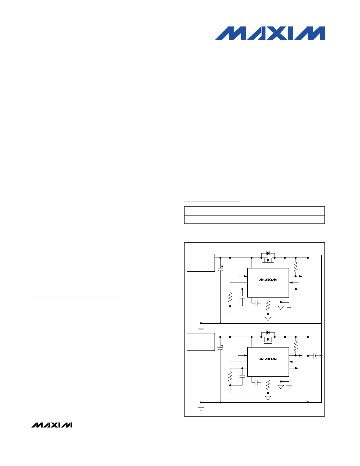
BUS
COMMON
GATE BUSIN
POWER SUPPLY 1
(PS1)
POWER SUPPLY 2
(PS2)
1V TO 13.2V
V
OUT1
V
OUT2
UVLO
OVI
GND
U1
STH
AUXIN
>2.75V
FTH
PGOOD
V
BUS
R
STH
R
FTH
R
FTH
C
STH
R
STH
C
STH
C
EXT
C
EXT
C
BUS
N1
V
IN
C+ C-
OVP
GATE BUSIN
1V TO 13.2V
UVLO
OVI
U2
STH
AUXIN
>2.75V
PGOOD
V
BUS
N2
V
IN
C+ C-
OVP
MAX5079
MAX5079
GNDFTH
SUB 75N 03-04
SUB 75N 03-04
Typical Operating Circuit
Pin Configuration appears at end of data sheet.
Page 2
MAX5079
ORing MOSFET Controller with
Ultra-Fast 200ns Turn-Off
2 _______________________________________________________________________________________
ABSOLUTE MAXIMUM RATINGS
ELECTRICAL CHARACTERISTICS
((VIN= 2.75V to 13.2V and V
AUXIN
= 0V) or (VIN= 1V and V
AUXIN
= 2.75V to 13.2V), R
STH
= open, R
FTH
= 0, V
UVLO
= 1V, V
OVI
= 0V,
T
A
= -40°C to +85°C, unless otherwise noted. Typical values are at VIN= 12V and TA= +25°C. See the Typical Operating Circuit.) (Note 1)
Stresses beyond those listed under “Absolute Maximum Ratings” may cause permanent damage to the device. These are stress ratings only, and functional
operation of the device at these or any other conditions beyond those indicated in the operational sections of the specifications is not implied. Exposure to
absolute maximum rating conditions for extended periods may affect device reliability.
GATE to GND ..............................................-0.3V to (VIN+ 8.5V)
All Other Pins to GND.............................................-0.3V to +15V
Continuous Current Into Any Pin ......................................±50mA
Continuous Power Dissipation (T
A
= +70°C)
14-Pin TSSOP (derate 9.1mW/°C above +70°C) ......727.3mW
Operating Temperature Range ...........................-40°C to +85°C
Junction Temperature......................................................+150°C
Storage Temperature Range .............................-65°C to +150°C
Lead Temperature (soldering, 10s) .................................+300°C
PARAMETER SYMBOL CONDITIONS
UNITS
POWER SUPPLIES
V
IN Input Voltage Range V
IN
V
AUXIN
≥ 2.75V 1.0
V
AUXIN Input Voltage Range V
AUXIN
0
V
(V
AUXIN
- VIN) High Threshold
(When GATE Connects Directly
to AUXIN) (Note 2)
V
AUXIN_
THRESHOLD
V
AUXIN
rising, I
GATE
= 10µA 4.3 4.9 5.4 V
(V
AUXIN
- VIN) Hysteresis (When
GATE Connects Directly To
AUXIN)
V
AUXIN_
HYSTERESIS
40 mV
IN Supply Current I
IN
V
UVLO
= 1V, VIN > V
BUS
4mA
AUXIN Leakage Current I
LEAK_AUX
V
AUXIN
= 0V 20 µA
AUXIN Supply Current I
AUXIN
V
UVLO
= 1V, V
AUXIN
= 13.2V, V
AUXIN
≥
V
IN
, V
AUXIN
≥ V
BUS
4mA
BUS Leakage Current I
LEAK_BUS
VIN = 13.2V, V
BUS
= 0V 1 mA
BUS Supply Current I
BUS
V
BUS
= 13.2V, V
BUS
> VIN, V
BUS
>
V
AUXIN
3mA
IN TO AUXIN SWITCHOVER
Switchover High Threshold
(VIN - V
AUXIN
), V
AUXIN
falling -60
mV
Switchover Low Threshold V
AUXIN_LOW
(VIN - V
AUXIN
), V
AUXIN
rising
-25
mV
IN UNDERVOLTAGE LOCKOUT
Internal UVLO High Threshold
VIN rising, V
AUXIN
= 0V or V
AUXIN
rising, VIN = 0V
2.0
2.5 V
Internal UVLO Hysteresis
VIN falling, V
AUXIN
= 0V or V
AUXIN
falling, VIN = 0V
30 mV
External UVLO Threshold V
UVLO
V
UVLO
falling
0.6
V
External UVLO Hysteresis V
UVLO_HYST
60 mV
External UVLO Input Bias
I
UVLO
500 nA
MIN TYP MAX
2.75 13.20
13.2
13.2
V
AUXIN_HIGH
V
INTUVLO_HIGH
V
INTUVLO_HYST
+25 +200
-200
2.25
0.568
+50
0.632
Page 3
MAX5079
ORing MOSFET Controller with
Ultra-Fast 200ns Turn-Off
_______________________________________________________________________________________ 3
ELECTRICAL CHARACTERISTICS (continued)
((VIN= 2.75V to 13.2V and V
AUXIN
= 0V) or (VIN= 1V and V
AUXIN
= 2.75V to 13.2V), R
STH
= open, R
FTH
= 0, V
UVLO
= 1V, V
OVI
= 0V,
T
A
= -40°C to +85°C, unless otherwise noted. Typical values are at VIN= 12V and TA= +25°C. See the Typical Operating Circuit.) (Note 1)
PARAMETER SYMBOL CONDITIONS
ORing MOSFET CONTROL
ORing MOSFET Turn-On Time t
ON
C
GATE
= 10nF, C
EXT
= 100nF,
MOSFET gate threshold = 2V
10 25 µs
ORing MOSFET Forward Voltage
Threshold (Fast Comparator)
V
DTH
(VIN - V
BUS
) rising 5
20 mV
R
FTH
= 0 -12 -24 -31
R
FTH
= 12kΩ -63
ORing MOSFET Reverse Voltage
Turn-Off Threshold (Fast
Comparator (V
IN
- V
BUS
))
V
FTH
R
FTH
= 27kΩ, VIN ≥ 3.5V
mV
ORing MOSFET Reverse Voltage
Blanking Time (Fast Comparator)
t
FBL
V
BUS
= 2.8V, R
FTH
= 0,
V
BUS
- VIN = 0.3V
50 ns
Slow-Comparator Output Voltage
Threshold on STH
V
O_STH
1
V
R
STH
open
-12
R
STH
= 500kΩ -25
ORing MOSFET Reverse Voltage
Turn-Off Threshold (Slow
Comparator (V
IN
- V
BUS
))
V
STH
R
STH
= 64kΩ
mV
(VIN - V
BUS
) to I
STH
Transconductance (Slow
Comparator)
G
M_STH
V
STH
= 0V
mS
STH floating 0.5 0.9 1.5
C
STH
= 0.047µF 5
ORing MOSFET Reverse Voltage
Blanking Time (Slow
Comparator)
t
SBL
C
STH
= 0.22µF 14
ms
ORing MOSFET DRIVER
Gate-Charge Current I
GATE
C
EXT
= 100nF 0.7 2 mA
V
GATE
≥ VIN, VIN = 5V, V
BUS
= 5V 0.9 2 5.0
1.3
Gate Discharge Current (Note 3)
3.2
A
V
BUS
= 3.5V, C
GATE
= 0.1µF
Gate Fall Time t
FGATE
V
BUS
= 3.5V, C
GATE
= 0.01µF
ns
Gate Discharge Current Delay
Time (Time from V
IN
Falling from
3.7V to 3V to V
GATE
= VIN)
t
DIS_GATE
V
BUS
= 3.5V, V
FTH
= 0V,
C
GATE
= 0.1nF
70 200 ns
Gate to IN Resistance R
GATE_IN
(V
GATE
- VIN) = 100mV 900 Ω
Gate to IN Clamp Voltage
I
GATE
= 10mA, VIN ≥ V
BUS
8.5 11 V
2.7V < VIN < 13.2V 3.8
VIN = 13.2V 6.5 7 7.6
Gate-Drive Voltage (Measured
with Respect to V
IN
)
VIN = 2.75V 4.5 5 5.5
V
VIN Switchover Threshold to
Higher GATE Voltage (Note 4)
V
IN_SOTH+
7.4 8 8.5 V
I
GATE.DIS_MIN
V
GAT E _ IN _ C L AM P
(V
- VIN)
GATE
MIN TYP MAX UNITS
12.5
-104 -150
-126 -204 -300
0.95
-0.1
-100
0.17
V
≥ VIN, VIN = 2.75V, V
GATE
V
GATE
≥ V
IN
, VIN = 12V, V
BUS
BUS
= 3.5V
= 13.2V
600
200
1.05
-24.0
Page 4
MAX5079
ORing MOSFET Controller with
Ultra-Fast 200ns Turn-Off
4 _______________________________________________________________________________________
Note 1: All devices are production tested at +25°C. Limits over temperature are guaranteed by design.
Note 2: Threshold is reached when charge pump turns off.
Note 3: Gate discharge current is guaranteed through the testing of gate fall time.
Note 4: V
IN
switchover threshold is VINat which the gate-drive voltage (V
GATE
- VIN) goes from 5V to 7V, VINrising and (VIN≥ V
BUS
).
ELECTRICAL CHARACTERISTICS (continued)
((VIN= 2.75V to 13.2V and V
AUXIN
= 0V) or (VIN= 1V and V
AUXIN
= 2.75V to 13.2V), R
STH
= open, R
FTH
= 0, V
UVLO
= 1V, V
OVI
= 0V,
T
A
= -40°C to +85°C, unless otherwise noted. Typical values are at VIN= 12V and TA= +25°C. See the Typical Operating Circuit.) (Note 1)
PARAMETER SYMBOL CONDITIONS
MIN
TYP
MAX
UNITS
VIN Switchover Hysteresis
(Note 4)
V
IN_SOHYS
40 mV
External 70
Charge-Pump Frequency f
CP
Internal, VIN < 5V, V
AUXIN
< 5V
kHz
PROTECTION
OVI Input Bias Current I
OVI
500 nA
OVI Threshold V
OVI_TH
OVI rising
0.6
V
OVP Output Low Voltage V
OVP_LOW
V
OVI
= 1V, I
SINK
= 10mA 0.2 0.4 V
OVP Leakage Current I
OVP_LEAK
VIN = 2.75V, V
OVP
= 13.2V 1 µA
PGOOD Leakage Current I
PG_LEAK
V
PGOOD
= 13.2V 1 µA
PGOOD Output Low Voltage V
PG_LOW
I
SINK
= 2mA 0.2 0.4 V
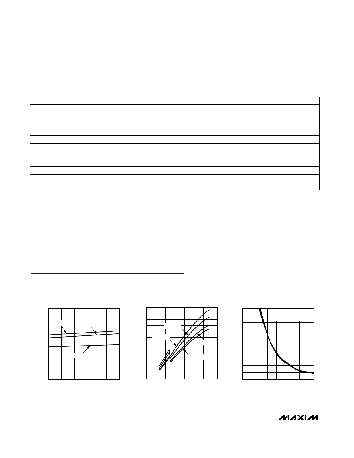
Typical Operating Characteristics
(TA = +25°C, unless otherwise noted. See the Typical Operating Circuit.)
AUXIN SUPPLY CURRENT
vs. TEMPERATURE (V
IN
= V
BUS
= 1V)
MAX5079 toc01
TEMPERATURE (°C)
I
AUXIN
(mA)
1109580655035205-10-25
1
2
3
0
-40 125
V
AUXIN
= 5V
V
AUXIN
= 10V
V
AUXIN
= 2.7V
GATE-CHARGE CURRENT vs. V
IN
MAX5079 toc02
VIN (V)
I
GATE
(mA)
14128 104 62
0.5
1.0
1.5
2.0
2.5
3.0
3.5
4.0
4.5
5.0
5.5
6.0
0
015
131179351
TA = +25°C
TA = -40°C
TA = +125°C
TA = +85°C
SLOW-COMPARATOR REVERSE VOLTAGE
THRESHOLD (V
STH
vs. R
STH
)
MAX5079 toc03
R
STH
(kΩ)
V
STH
(V)
100
0.02
0.04
0.06
0.08
0.10
0.12
0.14
0.16
0.18
0.20
0
10 1000
TA = -40°C, TA = +25°C,
T
A
= +85°C, TA = +125°C
1100
0.568
0.632
Page 5
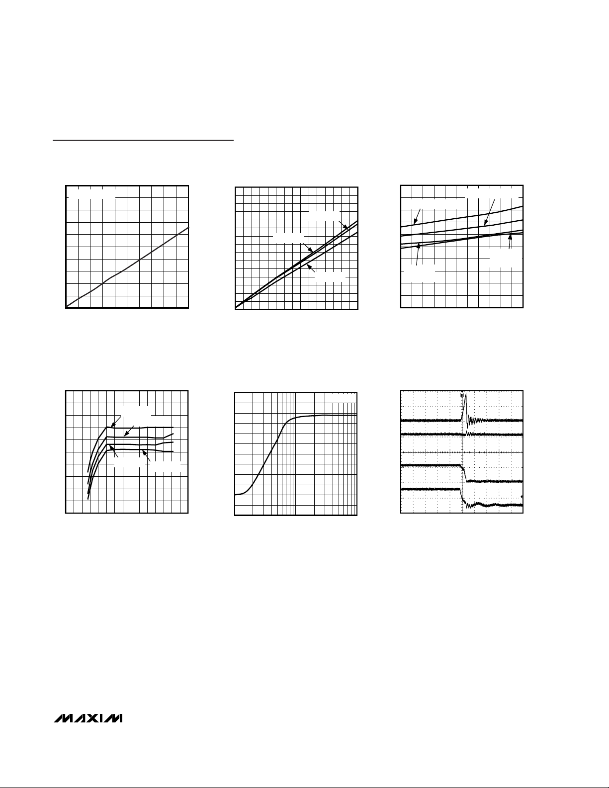
MAX5079
ORing MOSFET Controller with
Ultra-Fast 200ns Turn-Off
_______________________________________________________________________________________ 5
0
20
10
40
30
60
50
70
90
80
100
00.20.30.40.1 0.5 0.6 0.7 0.90.8 1.0
SLOW-COMPARATOR BLANKING TIME
t
STH
vs. C
STH
(R
STH
= 180kΩ)
MAX5079 toc04
C
STH
(µF)
t
STH
(ms)
75mV OVERDRIVE
FAST-COMPARATOR REVERSE VOLTAGE
THRESHOLD (V
FTH
vs. R
FTH)
MAX5079 toc05
R
FTH
(kΩ)
V
FTH
(V)
14012080 10040 6020
0.1
0.3
0.5
0.2
0.4
0.6
0.7
0.8
0.9
1.0
1.1
1.2
1.3
1.4
1.5
0
0
TA = +125°C
TA = +85°C
TA = -40°C
FAST-COMPARATOR RESPONSE TIME
MAX5079 toc06
TEMPERATURE (°C)
t
RESPONSE
(ns)
1109565 80-10 5 20 35 50-25
8
16
24
32
40
48
56
64
72
80
0
-40 125
VIN = 5V, V
AUXIN
= 0V
VIN = 1V, V
AUXIN
= 5V
VIN = 2.75V,
V
AUXIN
= 12V
VIN = 12V,
V
AUXIN
= 0V
CHARGE-PUMP FREQUENCY
vs. INPUT VOLTAGE
MAX5079 toc07
VIN (V)
f
CP
(kHz)
141210 11 1397 82 3 4 5 61
62
64
66
68
70
72
74
76
78
80
60
015
TA = +125°C
TA = +85°C
TA = +25°C
TA = -40°C
GATE-CHARGE CURRENT vs. C
EXT
MAX5079 toc08
C
EXT
(nF)
GATE-CHARGE CURRENT (mA)
10
0.5
1.0
1.5
2.0
2.5
3.5
4.0
4.5
5.0
6.0
0
1 100
VIN = 12V
3.0
5.5
FAULT CURRENT WAVEFORM
(IN SHORTED TO PGND)
MAX5079 toc09
VIN = 5V, V
BUS
= 5V,
V
AUXIN
= 0V, C
STH
= 0,
R
STH
= OPEN, R
FTH
= 0,
UVLO = IN
BUS
5V/div
IN
5V/div
GATE
10V/div
MOSFET REVERSE
CURRENT
5A/div
400ns/div
Typical Operating Characteristics (continued)
(TA = +25°C, unless otherwise noted. See the Typical Operating Circuit.)
Page 6
MAX5079
ORing MOSFET Controller with
Ultra-Fast 200ns Turn-Off
6 _______________________________________________________________________________________
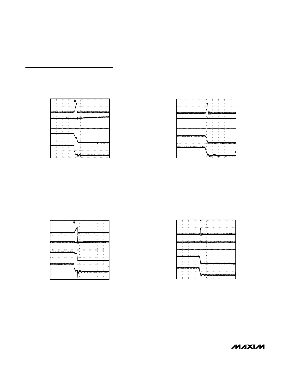
Typical Operating Characteristics (continued)
(TA = +25°C, unless otherwise noted. See the Typical Operating Circuit.)
FAULT CURRENT WAVEFORM
(IN SHORTED TO PGND)
MAX5079 toc13
VIN = 5V, V
BUS
= 5V,
V
AUXIN
= 5V, C
STH
= 0µF,
R
STH
= OPEN, R
FTH
= 0,
UVLO = IN
BUS
5V/div
IN
5V/div
GATE
10V/div
MOSFET REVERSE
CURRENT
10A/div
1µs/div
FAULT CURRENT WAVEFORM
(IN SHORTED TO PGND)
MAX5079 toc12
VIN = 1V, V
BUS
= 1V,
V
AUXIN
= 5V, C
STH
= 0µF,
R
STH
= OPEN, R
FTH
= 0,
UVLO = IN
BUS
1V/div
IN
1V/div
GATE
5V/div
MOSFET REVERSE
CURRENT
10A/div
1µs/div
FAULT CURRENT WAVEFORM
(IN SHORTED TO PGND)
MAX5079 toc10
VIN = 2.75V, V
BUS
= 2.75V,
V
AUXIN
= 0V, C
STH
= 0µF,
R
STH
= OPEN, R
FTH
= 0,
UVLO = IN
BUS
2V/div
IN
2V/div
GATE
5V/div
MOSFET REVERSE
CURRENT
10A/div
1µs/div
FAULT CURRENT WAVEFORM
(IN SHORTED TO PGND)
MAX5079 toc11
VIN = 12V, V
BUS
= 12V,
V
AUXIN
= 0V, C
STH
= 0µF,
R
STH
= OPEN, R
FTH
= 0,
UVLO = IN
BUS
10V/div
IN
10V/div
GATE
20V/div
MOSFET REVERSE
CURRENT
10A/div
400ns/div
Page 7

MAX5079
ORing MOSFET Controller with
Ultra-Fast 200ns Turn-Off
_______________________________________________________________________________________ 7
Typical Operating Characteristics (continued)
(TA = +25°C, unless otherwise noted. See the Typical Operating Circuit.)
FAULT CURRENT WAVEFORM
(IN SHORTED TO PGND)
MAX5079 toc14
VIN = 12V, V
BUS
= 12V,
V
AUXIN
= 5V, C
STH
= 0,
R
STH
= OPEN, R
FTH
= 0,
UVLO = IN
BUS
10V/div
IN
10V/div
GATE
20V/div
MOSFET REVERSE
CURRENT
10A/div
1µs/div
POWER-UP WAVEFORM
MAX5079 toc15
VIN = 5.2V, V
BUS
= 4.9V,
I
BUS
= 5A
BUS
2V/div
CXN
10V/div
GATE
10V/div
IN
2V/div
40µs/div
POWER-UP WAVEFORM
MAX5079 toc16
VIN = 12.2V, V
BUS
= 11.9V,
I
BUS
= 5A
BUS
5V/div
CXN
10V/div
GATE
10V/div
IN
5V/div
20µs/div
POWER-UP WAVEFORM
MAX5079 toc17
VIN = 1.2V, V
BUS
= 1V,
V
AUXIN
= 5V, I
BUS
= 5A
BUS
500mV/div
CXN
10V/div
GATE
5V/div
IN
1V/div
20µs/div
Page 8

MAX5079
ORing MOSFET Controller with
Ultra-Fast 200ns Turn-Off
8 _______________________________________________________________________________________
Pin Description
PIN NAME FUNCTION
1CXN Negative Terminal of External Flying Charge-Pump Capacitor
2 CXP Positive Terminal of External Flying Charge-Pump Capacitor
3 OVP
Open-Drain Active-Low Output. OVP sinks up to 10mA when V
OVI
≥ 0.6V and VIN ≥ V
BUS
. OVP can be
used to drive an optodiode. Cycle power or pull UVLO low and then high to reset OVP.
4PGOOD Open-Drain Active-Low Output. PGOOD pulls low when V
UVLO
≤ 0.6V or V
OVI
≥ 0.6V.
5 STH
ORing MOSFET Slow-Comparator Reverse Voltage Threshold and Blanking Time Setting Input. Connect
a resistor from STH to GND to set the threshold. Connect a capacitor from STH to GND to set the
blanking time. Leave STH floating to set the internal threshold (-12mV) and internal blanking time
(0.9ms).
6 FTH
Fast-Comparator Reverse Threshold Setting. Connect a resistor from FTH to GND to set the fastcomparator reverse voltage threshold from -24mV to -400mV.
7 OVI Overvoltage Comparator Input. Connect OVI to BUS through a resistive divider.
8 UVLO
Undervoltage Lockout Comparator Input. Connect UVLO to IN through a resistive divider. The MAX5079
remains off until V
UVLO
rises above 0.66V. When V
UVLO
rises above 0.664V, V
GATE
is raised to VIN.
9 PGND
Power Ground. Ground discharge path of the 2A GATE pulldown. Connect to external power ground
plane.
10 GATE Gate-Driver Output for n-Channel ORing MOSFET
11 BUS
Bus Voltage-Sense Input. Connect BUS to the drain of the ORing MOSFET to sense the polarity of the
Bus Current. The MAX5079 receives its power from BUS when V
IN
and V
AUXIN
are not present.
12 GND Signal Ground. Connect to the low-level signal or analog ground.
13 IN
Source Connection for ORing MOSFET and Supply Input for the MAX5079. Connect IN directly to the
power-supply voltage of 2.75V to 13.2V or 1V to 13.2V with V
AUXIN
≥ 2.75V.
14 AUXIN
Auxiliary Power-Supply Input. AUXIN supplies power to the IC when 1V ≤ V
IN
≤ 2.75V. Connect AUXIN to
2.75V or higher if V
IN
is less than 2.75V.
Page 9

MAX5079
ORing MOSFET Controller with
Ultra-Fast 200ns Turn-Off
_______________________________________________________________________________________ 9
AUXIN TO GATE
DIRECT CONNECTION
IN/AUXIN/BUS
SWITCHOVER
IN/AUXIN CHARGE-PUMP
SWITCHOVER
IN/AUXIN SUPPLY
SWITCHOVER
CHARGE
PUMP
0.6V
REFERENCE
IN
AUXIN
BUS
V
SUPPLY
UVLO
OVI
PGOOD
LOGIC
OV
LOGIC
INTERNAL
UVLO
OVP PGOOD
0.9ms
DELAY
TOP LOGIC
V
SUPPLY
CPOFF
UVLO OVI
N
PGND
CXP CXN GATE
PULLDOWN
REG
DRIVER
2A
PULLDOWN
PGOOD
GND
GATE TARGET SELECTOR
COMPARATOR
V
SUPPLY
V
SUPPLY
V
SUPPLY
V
SUPPLY
STH
20µA
G
M
HYSTERESIS
CONTROL
FTH
BUS
IN
MAX5079
Figure 1. Block Diagram
Block Diagram
Page 10

MAX5079
ORing MOSFET Controller with
Ultra-Fast 200ns Turn-Off
10 ______________________________________________________________________________________
Detailed Description
The MAX5079 ORing MOSFET controller drives an
external n-channel MOSFET and replaces ORing
diodes in high-reliability redundant power-management
systems or multiple paralleled power supplies. The
device has an internal charge pump to drive the highside n-channel ORing MOSFET. Additional features
include an adjustable undervoltage lockout threshold
(UVLO), output overvoltage detector (OVI/OVP), input
power-good detector (PGOOD), and two programmable reverse voltage detectors to detect both fast and
slow rises in the reverse voltage across the ORing
MOSFET. The input power-supply range is from 2.75V
to 13.2V or down to 1V when an auxiliary supply of at
least 2.75V is available.
Operational Description
This section describes a detailed startup sequence and
behavior of the MAX5079 under different conditions of
V
BUS
and VIN. The MAX5079 powers up whenever V
IN
is equal to or greater than 2.75V and V
UVLO
exceeds
the UVLO threshold of 0.66V. Operation with VINdown
to 1V is possible as long as V
UVLO
≥ 0.6V and V
AUXIN
≥
2.75V.
When V
UVLO
crosses the UVLO threshold, V
GATE
rises
to VINand the charge pump turns on. The charge
pump delivers 2mA to charge the gate capacitance of
the external MOSFET connected to GATE. The constant
gate-charge current prevents large inrush currents from
the input supply. During turn-on, the MAX5079 will
ignore the reverse voltage at IN with respect to BUS.
This is necessary to avoid the unintentional turn-off of
the ORing MOSFET as the momentary inrush current
causes VINto dip.
Figure 2 shows the MAX5079 in an ORing configuration
with three parallel power supplies (PS1, PS2, and PS3)
and three MAX5079s (U1, U2, and U3) provided by outputs V
OUT1
, V
OUT2
, and V
OUT3
. The following events
must be carefully considered to ensure proper functionality of the MAX5079 ICs.
1) V
BUS
is zero with a discharged capacitor (C
BUS
).
All three power supplies are turned ON simultaneously. V
OUT1
comes up before V
OUT2
and
V
OUT3
.
a. When V
OUT1
turns on, the bus capacitors (C
BUS
)
begin charging from V
OUT1
through N1’s body
diode. When V
UVLO
(U1) rises above the UVLO
threshold, the MAX5079 (U1) charge pump turns
on, and U1 monitors the positive potential from
V
OUT1
to V
BUS
. When V
OUT1
≥ V
BUS
the charge
pump brings GATE (U1) to 5.5V above VIN(U1) (or
7.5V above VINdepending on the magnitude of
VIN), by sourcing 2mA into N1’s gate capacitance.
This results in a less than 10µs turn-on time for the
FDB7045L used in the MAX5079 evaluation kit. The
fast turn-on is needed to assure that N1 is ON
before the rising V
OUT1
reaches its steady-state
value. If the MOSFET is not turned on before V
OUT1
reaches its steady state, V
BUS
may overshoot due
to the shorting of the 0.7V (forward drop) of N1’s
body diode. A higher VIN(U1) can more quickly
charge the charge-pump capacitor to 5V (or 7V),
while a lower VIN(U1) will take longer. Typically the
MOSFET turns on at VGS= 2.5V. Ensure that the
soft-start time of the power supply is large enough
(> 5ms) to avoid V
OUT1
racing ahead and causing
V
BUS
to overshoot. Care must be taken to avoid the
overloading of V
OUT1
by either limiting the source
current (using the current-sharing circuit) or delay
the loading of the BUS until all three power supplies
are up and running.
b. V
OUT2
turns on and begins increasing the voltage
at IN (U2). V
UVLO
(U2) crosses the UVLO threshold, the MAX5079 (U2) charge pump turns on and
U2 monitors the V
OUT2
to V
BUS
voltage. When this
voltage difference becomes positive, GATE (U2)
begins sourcing 2mA into N2’s gate capacitance.
During turn-on, the reverse voltage turn-off circuit
is momentarily disabled. If V
OUT2
is lower than
V
OUT1
, the external load-sharing controller circuit
of PS2 will try to increase V
OUT2
to source current
from V
OUT2
. Assume V
OUT2
’s rise time is slow
enough not to cause any overshoot before N2
turns on and starts sharing the current.
c. V
OUT3
turns on and U3 follows the same sequence
as U2. Eventually V
OUT1
, V
OUT2
, and V
OUT3
reach
to equilibrium and sharing equal currents.
2) PS1 and PS2 are on and sharing the load when
PS3 is hot-inserted. PS3 will take the same
course as discussed in 1b above.
a. If V
OUT3
is higher than V
BUS
, the BUS voltage will
increase to the new level determined by V
OUT3
.
The external load-sharing controller circuit of PS1
and PS2 will increase V
OUT1
and V
OUT2
to force
current sharing.
b. If V
OUT3
is lower than V
BUS
, the load-sharing cir-
cuit of PS3 will increase V
OUT3
to force the sharing
of current. This causes V
OUT3
to increases above
V
BUS
. When this voltage difference becomes positive, GATE (U3) begins sourcing 2mA into N3’s
gate capacitance. Again, the reverse voltage turnoff circuit is disabled momentarily, as discussed
before. The load-sharing circuit of PS3’s controller
will adjust V
OUT3
so as to share the load current.
Page 11

MAX5079
ORing MOSFET Controller with
Ultra-Fast 200ns Turn-Off
______________________________________________________________________________________ 11
c. During the hot insertion, a voltage spike can occur
at N1 and N2 and cause the (V
OUT1
to V
BUS
) or
(V
OUT2
to V
BUS
) voltage to go negative. If the
reverse voltage is below the fast-comparator
reverse voltage threshold (V
FTH
) but above the
programmed slow-comparator reverse voltage
threshold (V
STH
), the spike is ignored for the pro-
grammed blanking time (t
STH
). If the spike is
longer than 50ns (the fast-comparator internal
blanking time, t
FBL
) and larger than V
FTH
, then U1
and U2 will turn off N1 and N2 quickly. If the magnitude of the voltage spike is above V
STH
but less
than V
FTH
, and longer than the slow-comparator
blanking time (t
STH
), U1 and U2 will turn off their
respective ORing MOSFETs (N1 and N2) by discharging their GATE pins to PGND. The external
load-sharing circuit of PS1 and PS2 will force
V
OUT1
, V
OUT2
above V
BUS
and N1, N2 will turn
back on through the 2mA current sourcing from
the GATE pins of U1 and U2. To avoid this situation the user can set the slow-comparator threshold and blanking time depending on the
magnitude and duration of the voltage spikes.
d. PS3 fails to start. V
UVLO
(U3) threshold is not
crossed and U3 keeps N3 off.
e. PS3 goes into an overvoltage condition (no feed-
back). This causes V
BUS
to go into an overvoltage
condition increasing the loading on PS3 (provided
PS3 is able to supply all the required BUS current). The current-sharing circuit will force the outputs of PS1 and PS2 to increase and eventually
saturate at their current-sharing voltage range.
Eventually only PS3 will have a positive voltage at
IN (U3) with respect to BUS. PS1 and PS2 will
have a negative voltage at V
OUT1
and V
OUT2
with
respect to BUS. All overvoltage inputs OVI (U1),
OVI (U2), and OVI (U3) sense the overvoltage, but
only OVP (U3) is asserted and latched low. GATE
(U3) is pulled to PGND and remains low as long
as V
OVI
≥ 0.6V. When V
OVI
drops below 0.6V,
OVP remains low. However, U3 tries to turn on N3
unless V
OUT3
is actively kept below the undervoltage lockout. Use OVP (U3) to either drive the
cathode of the optocoupler to shutdown PS3 from
the primary side or use OVP (U3) to fire an SCR
connected between V
OUT3
and PGND.
3) PS1, PS2, PS3 are turned on with a shorted BUS.
Body diodes of N1, N2, and N3 conduct and short the
outputs of PS1, PS2, and PS3 to PGND. The power
supplies go into current limit (either in foldback or in
hiccup mode). The MAX5079s remain in undervoltage
lockout and keep all ORing MOSFETs off. The average
current sourced by PS1, PS2, or PS3 must be low
enough so as not to exceed the MOSFETs power dissipation (P
D
= VFx I
SHORT
).
a. Use additional n-channel MOSFETs in series with
N1, N2, and N3 in the reverse direction to isolate
the power supplies from a shorted bus (Figure 3).
When power is turned on with a shorted bus, V
IN_
(U1, U2, U3) increases and V
UVLO
rises above
the UVLO threshold. The MAX5079’s GATE outputs start charging the back-to-back ORing
MOSFET gates. The short-circuit condition at BUS
collapses VIN(U1), VIN(U2), and VIN(U3) sending the MAX5079s into undervoltage lockout. This
turns off the MAX5079s entirely, including discharging of the charge-pump storage capacitors.
The IN voltages come back up again crossing
UVLO (UVLO has 60mV hysteresis). A new cycle
starts and the time required to charge the chargepump capacitor and the turn-on time of the device
serves as a dead time. However, the dead time
may not be enough to reduce the dissipation in
the MOSFETs to an acceptable level. We advise
in keeping the short-circuit current low and providing hiccup current-limit protection to the power
supplies (PS1, PS2, and PS3).
b. Any other overload condition that would sustain the
IN voltage above UVLO, will keep the MOSFETs ON
continuously. Ensure the MOSFETs’ current
rating is higher than the maximum short-circuit
source current of the power supplies (PS1, PS2,
and PS3) to avoid damage to the ORing MOSFETs.
4) PS1, PS2, and PS3 are present and PS1 is shorted to GND.
V
OUT1
drops below V
BUS
. The negative potential from
V
IN
(U1) to V
BUS
increases above the fast-comparator
threshold and lasts longer than the 50ns blanking time.
The MAX5079 (U1) takes its power from the voltage at
BUS (U1). Connect BUS close to C
BUS
, away from N1
so that U1 can receive power from BUS for a few
microseconds until N1 isolates BUS from IN. N1 is discharged with 2A pulldown current, turning off N1 and
isolating PS1 from the BUS. The load-sharing circuit of
PS2 and PS3 will increase PS2 and PS3’s load current
until the total bus current requirement is satisfied.
For VIN(U1) < 2.75V, V
AUXIN
(U1) must come from an
independent source or remain on for some time (a few
microseconds) after VIN(U1) has failed. This minimum
on-time is needed to discharge the gate of the ORing
MOSFET and isolate PS1 from the BUS.
Page 12

MAX5079
ORing MOSFET Controller with
Ultra-Fast 200ns Turn-Off
12 ______________________________________________________________________________________
5) PS1, PS2, PS3 are present and PS1 goes open.
PS1’s output capacitors discharge and V
OUT1
drops
below V
BUS
. The MAX5079 (U1) senses a negative
potential from V
OUT1
to V
BUS
. Depending upon how
fast PS1’s output capacitor discharges, N1 is turned off
due to the crossing of the fast- or slow-comparator
reverse voltage threshold. N1’s gate is discharged with
a 2A sink current into GATE (U1), turning off N1 and
isolating PS1 from the BUS. The load-sharing circuit of
PS2 and PS3 will increase PS2 and PS3’s load current
until the total BUS current requirement is satisfied.
6) PS1, PS2, PS3 are present and providing BUS
current. PS1 loses its feedback signal and goes
into an overvoltage condition.
V
BUS
increases and PS1 is loaded heavily. The current
share circuit forces V
OUT2
and V
OUT3
higher and they
will eventually saturate at their current-sharing voltage
range. Now only PS1 has a positive voltage at IN (U1)
with respect to BUS. All OVI inputs will sense the overvoltage, but only OVP (U1) will be asserted and latched
low. GATE (U1) is pulled to PGND and remains low as
long as V
OVI
≥ 0.6V. When V
OVI
drops below 0.6V, OVP
remains low, however, U1 tries to turn on N1 unless
V
OUT1
is actively kept below the undervoltage lockout.
Use OVP (U1) to either drive the cathode of an optocoupler to shutdown PS1 from the primary, or fire an
SCR connected between IN (U1) and PGND.
Internal and External
Undervoltage Lockout
The internal undervoltage lockout monitors VINand
V
AUXIN
and keeps the MAX5079 off until either voltage
reaches 2.75V. Once powered and VINand/or V
AUXIN
increase above 2.75V, the external UVLO is monitored.
The external undervoltage lockout feature monitors the
UVLO input and keeps the MAX5079 off (GATE shorted
to PGND) until V
UVLO
is greater than 0.66V. Connect a
resistive divider from IN to UVLO to GND or from
AUXIN to UVLO to GND to set the external undervoltage lockout threshold. We advise setting the external
UVLO ≥ 2.75V when AUXIN is not present.
Charge Pump
The MAX5079 has an internal charge pump that pumps
the gate-drive voltage (V
GATE
) high enough to fully
enhance the n-channel ORing MOSFET. The charge
pump is divided into two stages, a voltage doubler running at 70kHz using an external charge-pump capacitor (C
EXT
), and a voltage tripler running at 1MHz using
an internal capacitor.
Connect an external capacitor (C
EXT
) between C+ and
C-. C
EXT
is charged from the higher of VINor V
AUXIN
.
When the rising VINbecomes greater then V
BUS(VUVLO
> 0.66V), C
EXT
is discharged through GATE into the
external MOSFET’s gate capacitance. The chargepump output is controlled by an internal regulator. The
charge-pump output at GATE sources typically 2mA.
This provides enough current drive to turn on a typical
ORing MOSFET in less than 10µs. When (V
GATE
- VIN)
reaches the target value (depending on VIN) the charge
pump is switched off (see the Electrical Characteristics
table). Choose C
EXT
equal to 10 times the ORing
MOSFET gate capacitance. Too low of a capacitance
will delay the turn-on of the ORing MOSFET, while too
high of a capacitance can cause excessive ripple at
VIN. Bypass IN to GND with a 1µF ceramic capacitor to
avoid ripple at IN caused by the charge-pump switching. A clamp is placed internally between GATE and IN
to prevent (V
GATE
- VIN) from exceeding 11V. When V
IN
is less than 5V, the charge pump (tripler) will increase
V
GATE
to 3x’s VINto further reduce the R
DSON
of the
ORing MOSFET. The internal charge-pump booster
(voltage tripler) section is operational only when VINand
V
AUXIN
are low and is turned off when VINexceeds 5V.
When an additional supply is connected to AUXIN and
(V
AUXIN
- VIN) > 5V, both charge pumps are completely
disabled. In this case, the charging of the ORing gate
comes entirely from V
AUXIN
. In this case, the chargepump flying capacitor can be eliminated and C+, Ccan be left floating.
GATE Drive and Gate Pulldown
The MAX5079’s charge pump provides bias to charge
the ORing MOSFET gate above IN (the MOSFET’s
source). GATE source current and the turn-on speed
depends upon the value of C
EXT
(connected between
C+ and C-). Typically GATE can source up to 2mA with
C
EXT
= 0.1µF. This enables V
GATE
to rise to over 2V
above VINin less than 10µs for an ORing MOSFET gate
capacitance of up to 10nF. With VIN< 5V, 12V MOSFETs
can be used for better R
DSON
characteristics. The
MAX5079 automatically selects the gate-drive voltage for
Page 13

MAX5079
ORing MOSFET Controller with
Ultra-Fast 200ns Turn-Off
______________________________________________________________________________________ 13
VIN= 5V or VIN= 12V. For VIN≤ 8V, the gate drive is 5V
above VINand for VIN> 8V, the gate drive is 7V above
VIN. Lower gate drive means faster turn-off during faults,
while higher gatedrive means lower R
DSON
.
A fast and slow comparator monitor the voltage from IN
to BUS. When this voltage crosses the negative fast- or
slow-comparator threshold voltage for the blanking time
duration, GATE is pulled low by an internal 2A current
sink. Both comparators have an adjustable threshold
voltage. GATE is pulled low if any of the following conditions are met.
1) V
UVLO
< 0.6V.
2) V
AUXIN
< 2.25V and VIN< 2.25V.
3) V
OVI
≥ 0.6V.
4) VIN≤ (V
BUS
- V
FTH
) or VIN≤ (V
BUS
- V
STH
) and
(V
GATE
- VIN) ≥ 1.8V.
When the above conditions are not true and VIN≤
V
BUS
, GATE is shorted to IN. To insure that the external
MOSFET is quickly turned off, given the above conditions, the GATE pulldown circuitry is powered by either
VIN, V
AUXIN
, or V
BUS
as long as any one is greater
then 2.75V.
Fast Comparator (FTH)
The fast comparator has a 50ns blanking time to avoid
unintentional turn-off of the ORing MOSFET during fast
transients. Additionally, the fast-comparator reverse
voltage threshold (V
FTH
) is programmable to suit the
need of an individual application. Higher V
FTH
threshold allows for a larger glitch at BUS during a fault, but
improves the noise immunity. Lower V
FTH
reduces
glitches at BUS during a fault, however, with lower V
FTH
spikes at BUS or glitches at IN can be read as faults,
unintentionally turning off the ORing MOSFET. Program
V
FTH
by connecting a resistor from FTH to GND. Adjust
V
FTH
to optimize the system performance using the fol-
lowing equation:
V
FTH
can be chosen from 24mV to 400mV. Connect
FTH to GND to choose the default 24mV threshold.
Slow Comparator (STH)
The MAX5079 includes a slow comparator to provide
glitch immunity during the hot insertion or removal of
paralleled power supplies. During the hot insertion,
BUS can see voltage spikes. These spikes can be
interpreted as a reverse voltage across the ORing
MOSFET. The amplitude of the spikes is proportional to
the load step seen by the parallel power supply while
the duration of the spikes depends on the loop
response of the load share and PWM controller.
The slow comparator has a programmable reverse voltage threshold (V
STH
) as well as a programmable blank-
ing time (t
STH
). An internal transconductance amplifier
converts the IN to BUS differential voltage to a current
and applies it to a parallel combination of resistor and
capacitor (R
STH
and C
STH
) from STH to GND. The
reverse threshold voltage (V
STH
) for the slow compara-
tor is adjusted through R
STH
. Use the following equa-
tion to calculate the R
STH
for a required V
STH
.
where G
M_STH
= 0.17mS.
The internal 500kΩ resistance from the output of the
transconductance to GND can change the actual V
STH
if R
STH
is above 50kΩ. In this case, see the Typical
Operating Circuit to select R
STH
. Once R
STH
is chosen,
the blanking time can be adjusted by C
STH
. The delay
time is:
where t
SBL
= 0.9ms and is the default blanking time
generated by an internal digital delay. Leaving STH
floating results in a 12mV threshold voltage and a 0.9ms
blanking time. VOD(overdrive) is the difference between
actual reverse voltage (V
BUS
- VIN) and V
STH
threshold.
Overvoltage Protection Latch (OVI/OVP)
OVI is the negative input to the overvoltage comparator. The positive input of this comparator is connected
to the internal 0.6V reference and an open-drain output
is provided at OVP. The overvoltage sensing for overvoltage protection is done at either IN or BUS. OVP
tRC
V
VV
t
DELAY STH STH
STH
STH DD
SBL
=××−−
+
+ln 1
R
V
VmVxG
STH
STH M STH
=
()
−
1
12
_
R
VmV
A
FTH
FTH
=
− 24
667. µ
Page 14

MAX5079
ORing MOSFET Controller with
Ultra-Fast 200ns Turn-Off
14 ______________________________________________________________________________________
latches low and the internal GATE pulldown circuitry is
activated and pulls GATE low only when both of the
conditions are satisfied:
1) V
OVI
≥ 0.6V.
2) VIN≥ V
BUS
.
OVP can sink 10mA maximum. Cycle power or pull
UVLO low and then high again to reset the OVP latch.
GATE is pulled to PGND and remains low as long as
V
OVI
≥ 0.6V. When V
OVI
drops below 0.6V, OVP remains
low. However, the MAX5079 tries to turn on the ORing
MOSFET unless VINis actively kept below the undervoltage lockout. Use OVP to drive the cathode of an optocoupler to shut down the respective power supply from
the primary side (see the Typical Application Circuit of
Figure 2) or fire an SCR connected from IN to PGND.
Power-Good Comparator (PGOOD)
PGOOD output pulls low when V
UVLO
falls below 0.6V
or V
OVI
goes above 0.6V. PGOOD can sink a maximum
of 2mA.
Layout Guidelines
1) Place a 1µF ceramic input bypass capacitor physically close to IN and PGND. Connect IN as close as
possible to the source of the ORing MOSFET.
2) Sense the V
BUS
close to the bulk capacitor, away from
the drain of the ORing MOSFET. When IN is shorted to
ground during a fault, BUS is also pulled low through
the ORing MOSFET. In the absence of V
AUXIN
, the
MAX5079 loses both power inputs VINand V
BUS
. This
can cause a delayed pulldown of the gate. Sensing
the BUS away from the ORing MOSFET drain, close to
the BUS bulk capacitor provides power to the
MAX5079 for a few microseconds, long enough to pull
down the ORing MOSFET gate and isolate BUS from a
shorted IN.
3) Place the charge-pump capacitor (C
EXT
) and the
slow-comparator blanking time adjustment capacitor
(C
STH
) as close as possible to the MAX5079.
4) Run a thick trace from the gate of the ORing MOSFET
to GATE.
Page 15

MAX5079
ORing MOSFET Controller with
Ultra-Fast 200ns Turn-Off
______________________________________________________________________________________ 15
Figure 2. Typical Application Circuit
BUS
COMMON
GATE BUSIN
POWER SUPPLY 1
(PS1)
TO PRIMARY-SIDE
SHUTDOWN
TO PRIMARY-SIDE
SHUTDOWN
POWER SUPPLY 2
(PS2)
1V TO 13.2V
V
OUT1
V
OUT2
UVLO
OVI
U1
N1
N2
STH
AUXIN
>2.75V
PGOOD
V
BUS
C
BUS
V
IN
C+ C-
MAX5079
OVP
GNDFTH
GATE BUSIN
1V TO 13.2V
UVLO
OVI
U2
STH
AUXIN
>2.75V
PGOOD
V
BUS
V
IN
C+ C-
MAX5079
OVP
GNDFTH
TO PRIMARY-SIDE
SHUTDOWN
POWER SUPPLY 3
(PS3)
V
OUT3
N3
GATE BUSIN
1V TO 13.2V
UVLO
OVI
U3
STH
AUXIN
>2.75V
PGOOD
V
BUS
V
IN
C+ C-
MAX5079
OVP
GNDFTH
C
STH
R
STH
C
EXT
R
FTH
R
FTH
C
STH
C
EXT
R
STH
V
BUS
V
BUS
R
FTH
C
STH
C
EXT
R
STH
V
BUS
Page 16

MAX5079
ORing MOSFET Controller with
Ultra-Fast 200ns Turn-Off
16 ______________________________________________________________________________________
Figure 3. Parallel Supplies with Back-to-Back MOSFET
BUS
COMMON
GATE BUSIN
POWER SUPPLY 1
(PS1)
TO PRIMARY-SIDE
SHUTDOWN
TO PRIMARY-SIDE
SHUTDOWN
POWER SUPPLY 2
(PS2)
1V TO 13.2V
V
OUT1
V
OUT2
UVLO
OVI
U1
STH
AUXIN
>2.75V
PGOOD
V
BUS
C
BUS
V
IN
C+ C-
MAX5079
OVP
GNDFTH
GATE BUSIN
1V TO 13.2V
UVLO
OVI
U2
STH
AUXIN
>2.75V
PGOOD
V
BUS
V
BUS
V
IN
C+ C-
MAX5079
OVP
GNDFTH
C
STH
R
STH
C
EXT
R
FTH
C
STH
R
STH
C
EXT
R
FTH
V
BUS
Page 17

MAX5079
ORing MOSFET Controller with
Ultra-Fast 200ns Turn-Off
______________________________________________________________________________________ 17
Chip Information
TRANSISTOR COUNT: 2,911
PROCESS: BiCMOS
14
13
12
11
10
9
8
1
2
3
4
5
6
7
AUXIN
IN
GND
BUSPGOOD
OVP
CXP
CXN
TOP VIEW
MAX5079
GATE
PGND
UVLOOVI
FTH
STH
TSSOP
Pin Configuration
Page 18

MAX5079
ORing MOSFET Controller with
Ultra-Fast 200ns Turn-Off
Maxim cannot assume responsibility for use of any circuitry other than circuitry entirely embodied in a Maxim product. No circuit patent licenses are
implied. Maxim reserves the right to change the circuitry and specifications without notice at any time.
18 ____________________Maxim Integrated Products, 120 San Gabriel Drive, Sunnyvale, CA 94086 408-737-7600
© 2005 Maxim Integrated Products Printed USA is a registered trademark of Maxim Integrated Products, Inc.
Package Information
(The package drawing(s) in this data sheet may not reflect the most current specifications. For the latest package outline information
go to www.maxim-ic.com/packages
.)
TSSOP4.40mm.EPS
 Loading...