

Page 1
General Description
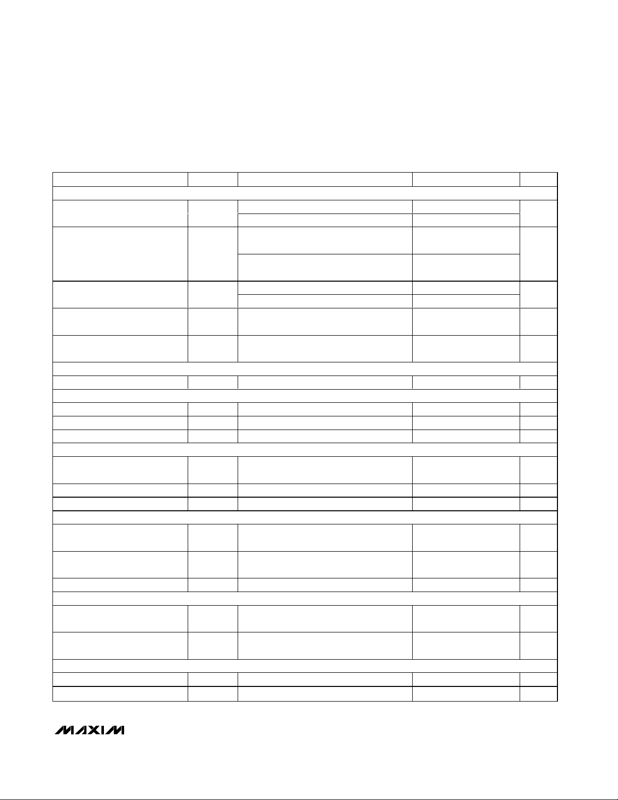
The MAX5074 isolated PWM power IC features integrated
switching power MOSFETs connected in a voltageclamped, two-transistor, power-circuit configuration. This
device can be used in both forward and flyback configurations with a wide input voltage range from 11V to 76V
and up to 15W of output power.
The voltage-clamped power topology enables full
recovery of stored magnetizing and leakage inductive
energy for enhanced efficiency and reliability. A lookahead signal for driving secondary-side synchronous
rectifiers can be used to increase efficiency.
A wide array of protection features includes UVLO,
overtemperature shutdown, and short-circuit protection
with hiccup current limit for enhanced performance and
reliability. Operation up to 500kHz allows smaller external magnetics and capacitors.
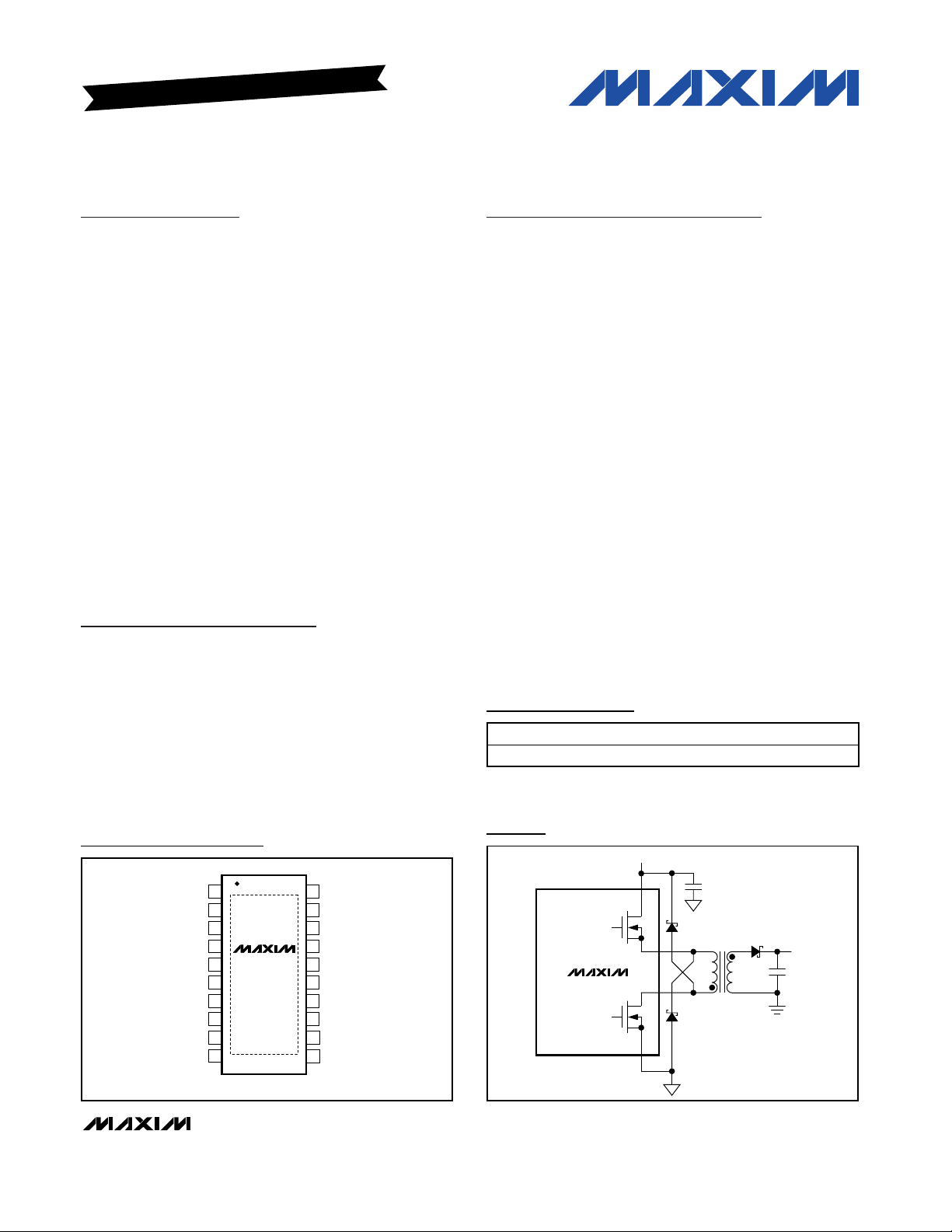
The MAX5074 is rated for operation over the -40°C to
+125°C temperature range and is available in a 20-pin
TSSOP package.
Warning: The MAX5074 is designed to work with
high voltages. Exercise caution.
Applications
IEEE 802.3af PD Power Supplies
Isolated IP Phone Power Supplies
High-Efficiency Telecom/Datacom Power Supplies
48V Input, Isolated Power-Supply Modules
WLAN Access-Point Power Supplies
ADSL Line Cards
ADSL Line-Driver Power Supplies
Distributed Power Systems with 48V Bus
Features
♦ Clamped, Two-Switch Power IC for High Efficiency
♦ No Reset Winding Required
♦ Up to 15W Output Power
♦ Bias Voltage Regulator with Automatic High-
Voltage Supply Turn-Off
♦ 11V to 76V Wide Input Voltage Range
♦ Integrated High-Voltage 0.4Ω Power MOSFETs
♦ Feed-Forward Voltage-Mode Control For Fast
Input Transient Rejection
♦ Programmable Brownout Undervoltage Lockout
♦ Internal Overtemperature Shutdown
♦ Indefinite Short-Circuit Protection With
Programmable Fault Integration
♦ Integrated Look-Ahead Signal for Secondary-Side
Synchronous Rectification
♦ >90% Efficiency with Synchronous Rectification
♦ Up to 500kHz Switching Frequency
♦ High-Power (1.74W), Small-Footprint 20-Pin
Thermally Enhanced TSSOP Package
MAX5074
Power IC with Integrated MOSFETs for Isolated IEEE
802.3af PD and Telecom Power-Supply Applications
________________________________________________________________ Maxim Integrated Products 1
Pin Configuration
Ordering Information
MAX5074
DRNH
SRC
DRVL
DRVH
QH
QL
D2
D1
D3
T1
V
IN
C
IN
C
OUT
V
OUT
XFRMRH
XFRMRL
Simplified Application Circuit
19-3312; Rev 0; 7/04
For pricing, delivery, and ordering information, please contact Maxim/Dallas Direct! at
1-888-629-4642, or visit Maxim’s website at www.maxim-ic.com.
*EP = Exposed pad.
EVALUATION KIT AVAILABLE
20
INBIAS
19
HVIN
18
UVLO
17
BSTRCFF
MAX5074
TSSOP
DRNH
16
XFRMRH
15
14
DRVIN
XFRMRLPPWM
13
12
SRC
11
PGNDCS
TOP VIEW
1
REGOUT
2
RTCT
3
FLTINT
4
RAMP
5
OPTO
6
CSS
7
8
9
GND
10
PART TEMP RANGE PIN-PACKAGE
MAX5074AUP -40°C to +125°C 20-TSSOP-EP*
Page 2

MAX5074
Power IC with Integrated MOSFETs for Isolated IEEE
802.3af PD and Telecom Power-Supply Applications
2 _______________________________________________________________________________________
ABSOLUTE MAXIMUM RATINGS
ELECTRICAL CHARACTERISTICS
(V
HVIN
= 12V, C
INBIAS
= 1µF, C
REGOUT
= 2.2µF, R
RTCT
= 25kΩ, C
RTCT
= 100pF, C
BST
= 0.22µF, V
CSS
= VCS= 0V, V
RAMP
= V
UVLO
= 3V,
T
A
= TJ= -40°C to +125°C, unless otherwise noted. Typical values are at TA= +25°C, unless otherwise noted.) (Note 1)
Stresses beyond those listed under “Absolute Maximum Ratings” may cause permanent damage to the device. These are stress ratings only, and functional
operation of the device at these or any other conditions beyond those indicated in the operational sections of the specifications is not implied. Exposure to
absolute maximum rating conditions for extended periods may affect device reliability.
HVIN, INBIAS, DRNH, XFRMRH,
XFRMRL to GND.................................................-0.3V to +80V
BST to GND ............................................................-0.3V to +95V
BST to XFRMRH .....................................................-0.3V to +12V
PGND to GND .......................................................-0.3V to +0.3V
UVLO, RAMP, CSS, OPTO, FLTINT, RCFF,
RTCT to GND......................................................-0.3V to +12V
SRC, CS to GND.......................................................-0.3V to +6V
REGOUT, DRVIN to GND .......................................-0.3V to +12V
REGOUT to HVIN ...................................................-80V to +0.3V
REGOUT to INBIAS ................................................-80V to +0.3V
REGOUT Current ................................................................50mA
PPWM to GND....................................-0.3V to (REGOUT + 0.3V)
PPWM Current .................................................................±20mA
DRNH, XFRMRH, XRFMRL, SRC Continuous Current (Average)
T
J
= +125°C......................................................................0.9A
T
J
= +150°C......................................................................0.6A
Continuous Power Dissipation (T
A
= +70°C)
20-Pin TSSOP-EP (derate 21.7mW/°C above +70°C) ....1.739W
20-Pin TSSOP-EP (θ
JA
) ................................................46°C/W
Operating Temperature Range .........................-40°C to +125°C
Maximum Junction Temperature .....................................+150°C
Storage Temperature Range .............................-60°C to +150°C
Lead Temperature (soldering, 10s) .................................+300°C
Input Supply Range V
OSCILLATOR (RTCT)
PWM Frequency f
Maximum PWM Duty Cycle D
Maximum RTCT Frequency f
RTCT Peak Trip Level V
RTCT Valley Trip Level
RTCT Input Bias Current ±1 µA
RTCT Discharge MOSFET
R
DS(ON)
RTCT Discharge Pulse Width 50 ns
LOOK-AHEAD LOGIC (PPWM)
PPWM to XFRMRL Output
Propagation Delay
PPWM Output High V
PPWM Output Low V
PWM COMPARATOR (OPTO, RAMP, RCFF)
Common-Mode Range V
Input Offset Voltage 10 mV
Input Bias Current -2 +2 µA
RAMP to XFRMRL Propagation
Delay
Minimum OPTO Voltage V
Minimum RCFF Voltage RCFF sinking 2mA 2.18 V
PARAMETER SYMBOL CONDITIONS MIN TYP MAX UNITS
HVIN
S
MAX
RTCTMAX
TH
t
PPWM
OH
OL
CM-PWM
R
= 25kΩ, C
RTCT
R
= 25kΩ, C
RTCT
(Note 2) 1 MHz
Sinking 20mA 30 60 Ω
PPWM rising to XFRMRL falling 110 ns
Sourcing 2mA 7.0 11.0 V
Sinking 2mA 0.4 V
From RAMP (50mV overdrive) rising to
XFRMRL rising
= 0V, OPTO sinking 2mA 1.47 V
CSS
RTCT
RTCT
= 100pF 256 kHz
= 100pF 47 %
11 76 V
0.51 x
V
REGOUT
0.04 x
V
REGOUT
0 5.5 V
100 ns
V
V
Page 3
MAX5074
Power IC with Integrated MOSFETs for Isolated IEEE
802.3af PD and Telecom Power-Supply Applications
_______________________________________________________________________________________ 3
ELECTRICAL CHARACTERISTICS (continued)
(V
HVIN
= 12V, C
INBIAS
= 1µF, C
REGOUT
= 2.2µF, R
RTCT
= 25kΩ, C
RTCT
= 100pF, C
BST
= 0.22µF, V
CSS
= VCS= 0V, V
RAMP
= V
UVLO
= 3V,
T
A
= TJ= -40°C to +125°C, unless otherwise noted. Typical values are at TA= +25°C, unless otherwise noted.) (Note 1)
)
PARAMETER SYMBOL CONDITIONS MIN TYP MAX UNITS
REGOUT LDO (REGOUT)
REGOUT Voltage Set Point V
REGOUT Load Regulation
REGOUT Dropout Voltage
REGOUT Undervoltage Lockout
Threshold
REGOUT Undervoltage Lockout
Threshold Hysteresis
SOFT-START (CSS)
Soft-Start Current I
INTEGRATING FAULT PROTECTION (FLTINT)
FLTINT Source Current I
FLTINT Trip Point FLTINT rising 2.7 V
FLTINT Hysteresis 0.8 V
INTERNAL POWER MOSFETs (See Figure 1, QH and QL)
On-Resistance R
Off-State Leakage Current -5 +5 µA
Total Gate Charge Per FET 15 nC
HIGH-SIDE DRIVER
Low-to-High Delay
High-to-Low Delay
Driver Output Voltage BST to XFRMRH with high side on 8 V
LOW-SIDE DRIVER
Low-to-High Delay
High-to-Low Delay
CURRENT-LIMIT COMPARATOR (CS)
Current-Limit Threshold Voltage V
Current-Limit Input Bias Current I
REGOUT
CSS
FLTINT
DS(ON
ILIM
BILIM
INBIAS floating, V
V
= V
INBIAS
INBIAS floating, V
to 30mA
V
= V
INBIAS
30mA
INBIAS floating, I
= V
V
INBIAS
= 11V to 76V 8.3 9.2
HVIN
= 11V to 76V 9.5 11.0
HVIN
= 15V, I
HVIN
= 15V, I
HVIN
HVIN
, I
REGOUT
= 30mA 1.25
REGOUT
= 30mA 1.25
REGOUT
REGOUT
= 0 to
= 0
0.25
0.25
REGOUT rising 6.6 7.4 V
REGOUT falling 0.7 V
33 µA
80 µA
V
= V
DRVIN
V
XFRMRH
Driver delay until FET V
- V
(V
BST
Driver delay until FET V
- V
(V
BST
Driver delay until FET V
V
DRVIN
Driver delay until FET V
V
DRVIN
= 9V,
BST
= V
= 0V, IDS = 50mA
SRC
) and is fully on
XFRMRH
) and is fully off
XFRMRH
and is fully on
and is fully off
reaches 0.9 x
GS
reaches 0.1 x
GS
reaches 0.9 x
GS
reaches 0.1 x
GS
0.4 0.8 Ω
80 ns
40 ns
80 ns
40 ns
140 156 172 mV
0 < VCS < 0.3V -2 +2 µA
V
V
V
Page 4
MAX5074
Power IC with Integrated MOSFETs for Isolated IEEE
802.3af PD and Telecom Power-Supply Applications
4 _______________________________________________________________________________________
ELECTRICAL CHARACTERISTICS (continued)
(V
HVIN
= 12V, C
INBIAS
= 1µF, C
REGOUT
= 2.2µF, R
RTCT
= 25kΩ, C
RTCT
= 100pF, C
BST
= 0.22µF, V
CSS
= VCS= 0V, V
RAMP
= V
UVLO
= 3V,
T
A
= TJ= -40°C to +125°C, unless otherwise noted. Typical values are at TA= +25°C, unless otherwise noted.) (Note 1)
Note 1: All limits at -40°C are guaranteed by design and not production tested.
Note 2: Output switching frequency is half of oscillator frequency.
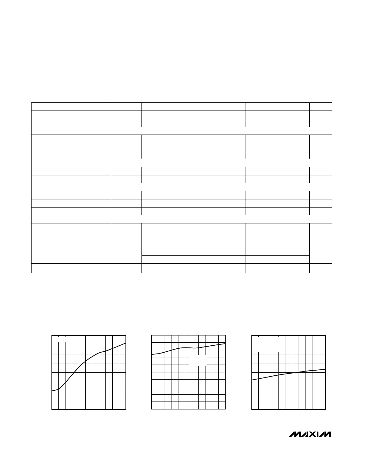
UNDERVOLTAGE LOCKOUT THRESHOLD
vs. TEMPERATURE
MAX5074 toc01
TEMPERATURE (°C)
V
UVLO
(V)
11095-25 -10 5 35 50 6520 80
1.2425
1.2450
1.2475
1.2500
1.2525
1.2550
1.2575
1.2600
1.2400
-40 125
UVLO RISING
STANDBY CURRENT vs. TEMPERATURE
MAX5074 toc02
TEMPERATURE (°C)
STANDBY CURRENT (µA)
1109565 80-10 5 20 35 50-25
35
70
105
140
175
210
245
280
315
350
0
-40 125
I
HVIN
V
UVLO =
0V
HVIN INPUT CURRENT
vs. TEMPERATURE
MAX5074 toc03
TEMPERATURE (°C)
I
HVIN
(mA)
11095-25 -10 5 35 50 6520 80
4.1
4.2
4.3
4.4
4.5
4.6
4.7
4.8
4.0
-40 125
V
HVIN
= 76V
INBIAS FLOATING
REGOUT = DRVIN
Typical Operating Characteristics
(V
HVIN
= 48V, V
INBIAS
= 15V, C
INBIAS
= 1µF, C
REGOUT
= 2.2µF, R
RTCT
= 25kΩ, C
RTCT
= 100pF, C
BST
= 0.22µF, V
CSS
= VCS= 0V,
V
RAMP
= V
UVLO
= 3V, TA = TJ= -40°C to +125°C, unless otherwise noted. Typical values are at TA= +25°C, unless otherwise noted.)
PARAMETER SYMBOL CONDITIONS MIN TYP MAX UNITS
Propagation Delay to XFRMRL t
BOOST VOLTAGE CIRCUIT (See Figure 1, QB)
Driver Output Delay t
One-Shot Pulse Width t
QB R
DS(ON)
THERMAL SHUTDOWN
Shutdown Temperature T
Thermal Hysteresis T
UNDERVOLTAGE LOCKOUT (UVLO)
UVLO Threshold V
UVLO Hysteresis V
UVLO Input Bias Current I
SUPPLY CURRENT
Supply Current
Standby Supply Current V
dILIM
PPWMD
PWQB
SH
HYST
UVLO
HYST
BUVLO
From CS rising (10mV overdrive) to
XFRMRL rising
160 ns
200 ns
300 ns
Sinking 20mA 30 60 Ω
Temperature rising +160 °C
15 °C
V
rising 1.14 1.38 V
UVLO
140 mV
V
= 3V -100 +100 nA
UVLO
From V
V
INBIAS
From V
V
HVIN
From V
UVLO
= 11V to 76V, V
HVIN
= 11V
= 11V to 76V, V
INBIAS
= 76V
= 76V 7
HVIN
CSS
CSS
= 0V,
= 0V,
0.7 2
4.4 6.0
= 0V 1 mA
mA
Page 5

MAX5074
Power IC with Integrated MOSFETs for Isolated IEEE
802.3af PD and Telecom Power-Supply Applications
_______________________________________________________________________________________ 5
Typical Operating Characteristics (continued)
(V
HVIN
= 48V, V
INBIAS
= 15V, C
INBIAS
= 1µF, C
REGOUT
= 2.2µF, R
RTCT
= 25kΩ, C
RTCT
= 100pF, C
BST
= 0.22µF, V
CSS
= VCS= 0V,
V
RAMP
= V
UVLO
= 3V, TA = TJ= -40°C to +125°C, unless otherwise noted. Typical values are at TA= +25°C, unless otherwise noted.)
REGOUT VOLTAGE vs. TEMPERATURE
8.800
V
= 76V
HVIN
INBIAS FLOATING
8.775
8.750
8.725
(V)
8.700
REGOUT
V
8.675
8.650
8.625
8.600
-40 125
REGOUT VOLTAGE vs. LOAD CURRENT
8.75
V
= 15V
HVIN
INBIAS FLOATING
8.70
(V)
8.65
REGOUT
V
8.60
8.55
030
REGOUT VOLTAGE vs. INPUT VOLTAGE
8.75
INBIAS FLOATING
MAX5074 toc04
8.73
8.71
(V)
REGOUT
V
8.69
8.67
8.65
11095-25 -10 5 35 50 6520 80
TEMPERATURE (°C)
11 76
HVIN AND INBIAS INPUT CURRENT
5.0
4.5
MAX5074 toc07
4.0
3.5
3.0
(mA)
2.5
HVIN
I
2.0
1.5
1.0
0.5
0
-40 125
I
REGOUT
252015105
(mA)
vs. TEMPERATURE
TEMPERATURE (°C)
V
HVIN
I
HVIN
V
HVIN
I
V
(V)
INBIAS
= V
HVIN
= V
INBIAS
INBIAS
63503724
= 76V
= 76V
1109565 80-10 5 20 35 50-25
7.50
7.25
MAX5074 toc05
7.00
6.75
6.50
REGOUT UVLO VOLTAGE (V)
6.25
6.00
-40 125
REGOUT VOLTAGE vs. TEMPERATURE
10.60
10.59
MAX5074 toc08
10.58
10.57
10.56
(V)
10.55
REGOUT
V
10.54
10.53
10.52
10.51
10.50
-40 125
REGOUT UVLO VOLTAGE
vs. TEMPERATURE
RISING
FALLING
TEMPERATURE (°C)
V
= V
HVIN
= 76V
INBIAS
TEMPERATURE (°C)
MAX5074 toc06
1109580655035205-10-25
MAX5074 toc09
1109565 80-10 5 20 35 50-25
REGOUT VOLTAGE vs. INPUT VOLTAGE
10.60
HVIN = INBIAS
10.58
10.56
(V)
REGOUT
V
10.54
10.52
10.50
11 76
V
(V)
HVIN
MAX5074 toc10
63503724
REGOUT VOLTAGE vs. LOAD CURRENT
10.60
V
= V
INBIAS
= 15V
I
REGOUT
MAX5074 toc11
252015105
(mA)
HVIN
10.55
(V)
10.50
REGOUT
V
10.45
10.40
030
Page 6

MAX5074
Power IC with Integrated MOSFETs for Isolated IEEE
802.3af PD and Telecom Power-Supply Applications
6 _______________________________________________________________________________________
Typical Operating Characteristics (continued)
(V
HVIN
= 48V, V
INBIAS
= 15V, C
INBIAS
= 1µF, C
REGOUT
= 2.2µF, R
RTCT
= 25kΩ, C
RTCT
= 100pF, C
BST
= 0.22µF, V
CSS
= VCS= 0V,
V
RAMP
= V
UVLO
= 3V, TA = TJ= -40°C to +125°C, unless otherwise noted. Typical values are at TA= +25°C, unless otherwise noted.)
OPERATING FREQUENCY
vs. TEMPERATURE
MAX5074 toc12
TEMPERATURE (°C)
OPERATING FREQUENCY (kHz)
11095-25 -10 5 35 50 6520 80
250
300
350
400
450
500
550
600
200
-40 125
R
RTCT
= 12kΩ
C
RTCT
= 100pF
R
RTCT
= 25kΩ
C
RTCT
= 100pF
SOFT-START CURRENT
vs. TEMPERATURE
MAX5074 toc13
TEMPERATURE (°C)
SOFT-START CURRENT (µA)
11095-25 -10 5 35 50 6520 80
31.25
31.50
31.75
32.00
32.25
32.50
32.75
33.00
31.00
-40 125
MINIMUM RCFF AND OPTO LEVELS
vs. TEMPERATURE
MAX5074 toc14
TEMPERATURE (°C)
V
RCFF
(V), V
OPTO
(V)
11095-25 -10 5 35 50 6520 80
1.25
1.50
1.75
2.00
2.25
2.50
2.75
3.00
1.00
-40 125
OPTO
RCFF
CURRENT-LIMIT COMPARATOR
THRESHOLD vs. TEMPERATURE
MAX5074 toc15
TEMPERATURE (°C)
V
REGOUT
(mV)
1109565 80-10 5 20 35 50-25
151
152
153
154
155
156
157
158
159
160
150
-40 125
HVIN RISING
PPWM TO XFRMRL SKEW
vs. TEMPERATURE
MAX5074 toc16
TEMPERATURE (°C)
PPWM TO XFRML SKEW (ns)
1109565 80-10 5 20 35 50-25
106
107
108
109
110
111
112
113
114
115
105
-40 125
FLTINT CURRENT vs. TEMPERATURE
MAX5074 toc17
TEMPERATURE (°C)
I
FLTINT
(µA)
1109565 80-10 5 20 35 50-25
76
77
78
79
80
81
82
83
84
85
75
-40 125
FLTINT SHUTDOWN
VOLTAGE vs. TEMPERATURE
MAX5074 toc18
TEMPERATURE (°C)
V
FLTINT
(V)
1109565 80-10 5 20 35 50-25
1.9
2.0
2.1
2.2
2.3
2.4
2.5
2.6
2.7
2.8
1.8
-40 125
FALLING
RISING
POWER MOSFETS R
DS(ON)
vs. TEMPERATURE
MAX5074 toc19
TEMPERATURE (°C)
R
DS(ON)
(Ω)
1109565 80-10 5 20 35 50-25
0.25
0.30
0.35
0.40
0.45
0.50
0.55
0.60
0.65
0.70
0.20
-40 125
Page 7

MAX5074
Power IC with Integrated MOSFETs for Isolated IEEE
802.3af PD and Telecom Power-Supply Applications
_______________________________________________________________________________________ 7
Pin Description
PIN NAME FUNCTION
1 REGOUT
2 RTCT
3 FLTINT
4 RCFF
5 RAMP PWM Ramp Sense Input. Connect RAMP to RCFF.
6 OPTO
7 CSS Soft-Start and Reference. Connect a 10nF or greater capacitor from CSS to GND.
8 PPWM PWM Pulse Output. PPWM leads the internal power MOSFET pulse by approximately 100ns.
9 GND Signal Ground. Connect GND to PGND.
10 CS
11 PGND Power Ground. Connect PGND to GND.
12 SRC
13 XFRMRL Low-Side Connection for the Isolation Transformer
14 DRVIN
15 XFRMRH High-Side Connection for the Isolation Transformer
16 DRNH
Regulator Output. Always present as long as HVIN is powered with a voltage above UVLO threshold.
Bypass REGOUT to GND with a minimum 2.2µF ceramic capacitor.
Oscillator Frequency Set Input. Connect a resistor from RTCT to REGOUT and a capacitor from RTCT to
GND to set the oscillator frequency.
Fault Integration Input. During persistent current-limit faults, a capacitor connected to FLTINT is charged
with an internal 80µA current source. Switching is terminated when V
resistor connected in parallel discharges the capacitor. Switching resumes when V
Feed-Forward Input. To generate the PWM ramp, connect a resistor from RCFF to HVIN and a capacitor
from RCFF to GND.
PWM Comparator Inverting Input. Connect the collector of the optotransistor to OPTO and a pullup resistor
to REGOUT.
Current-Sense Input. The current-limit threshold is internally set to 156mV relative to PGND. The device has
an internal noise filter. If necessary, connect an external RC filter for additional filtering.
Internal Low-Side Power MOSFET Source. Connect SRC to PGND with a low-value resistor for current
limiting.
MOSFET Gate-Driver Supply Input. Bypass DRVIN with at least 0.1µF to PGND. Connect DRVIN to
REGOUT.
Drain Connection of the Internal High-Side PWM Power MOSFET. Connect DRNH to the most positive rail
of the input supply. Bypass DRNH appropriately to handle the heavy switching current through the
transformer.
reaches 2.7V. An external
FLTINT
FLTINT
drops to 1.9V.
17 BST
18 UVLO
19 HVIN High-Voltage Input. Connect HVIN to the most positive input supply rail.
20 INBIAS Input from the Rectified Bias Winding. INBIAS is an input to the internal linear voltage regulator (REGOUT).
—EP
Boost Input. BST is the boost connection point for the high-side MOSFET driver. Connect a minimum
0.1µF capacitor from BST to XFRMRH with short and wide PC board traces.
Undervoltage Lockout Input. Connect a resistive divider from HVIN to UVLO and from UVLO to GND to set
the UVLO threshold.
Exposed Paddle. EP is internally connected to GND. Connect the exposed paddle to a copper pad to
improve power dissipation.
Page 8

MAX5074
Detailed Description
The MAX5074 PWM power IC is the primary-side
controller for voltage-mode, isolated forward or flyback
power converters. This device provides a high degree of
integration aimed at reducing the cost and printed circuit
board area of isolated output power supplies. Use the
MAX5074 primarily in 48V power bus applications.
The MAX5074 is a complete power IC capable of delivering up to 15W of output power. This device contains PWM
circuitry and integrated power MOSFETs. Figure 1 shows
the MAX5074’s block diagram. The MAX5074 includes
undervoltage lockout, overtemperature shutdown, and
short-circuit protection for enhanced performance and
reliability. Operation up to 500kHz allows the use of small
external magnetics and capacitors.
Power IC with Integrated MOSFETs for Isolated IEEE
802.3af PD and Telecom Power-Supply Applications
8 _______________________________________________________________________________________
Figure 1. Block Diagram
IFLT
50Ω
REGOK
CPWM
OVRLD
GND
REG
OVT
REFOK
5V
7.5V
D
Q
T
R
CLK
OVT
UVLO
REFOK
REGOK
OVRLD
GND
50Ω
Q
R
T-FF
14REGOUT
RCFF
80µA
3
FLTINT
5
RAMP
6
OPTO
33µA
79CSS
GND
5V
2.7V/1.9V
5V
MAX5074
REF
(1.25V)
R
S
T
Q
ILIM
SHDN
OSC
UVLO
CUVLO
THERMAL
SHUTDOWN
80ns
DELAY
10MHz
OVT
1.25V
LEVEL
SHIFT
LEADING-
EDGE
DELAY
ONE
SHOT
30Ω
0.4Ω
QB
0.4Ω
QH
QL
INBIAS
HVIN
UVLO
PPWM
BST
DRNH
XFRMRH
DRVIN
XFRMRL
SRC
PGND
RTCT
20
19
18
8
17
16
15
14
13
12
11
2
CS
10
150mV
PGND
Page 9

Power Topology
The two-switch forward converter topology offers outstanding robustness against faults and transformer
saturation while affording efficient use of the integrated
0.4Ω power MOSFETs. Voltage-mode control with
feed-forward compensation allows the rejection of
input supply disturbances within a single cycle similar
to that of current-mode controlled topologies.
The two-switch power topology recovers energy stored
in both the magnetizing and the parasitic leakage
inductances of the transformer. The Typical Application
Circuit, forward converter (Figure 3) shows the
schematic diagram of a 48V input and 5V, 3A output
isolated power supply. Figure 4 shows the schematic
diagram of a flyback converter using the MAX5074.
Undervoltage Lockout (UVLO)
The UVLO block monitors the input voltage HVIN
through an external resistive divider (R24 and R25)
connected to UVLO (see Figure 3). Use the following
equation to calculate R24 and R25:
where V
UVLOIN
is the desired input voltage lockout
level and V
UVLO
is the undervoltage lockout threshold
(1.25V, typ).
Internal Regulators
As soon as power is provided to HVIN, internal power
supplies power the UVLO detection circuitry. REGOUT is
used to drive the internal power MOSFETs. Bypass
REGOUT with a minimum 2.2µF ceramic capacitor. The
HVIN LDO steps down V
HVIN
to a nominal output voltage
(REGOUT) of 8.75V. A second parallel LDO powers
REGOUT from INBIAS. A tertiary winding connected
through a diode to INBIAS powers up REGOUT once
switching commences. This will bring REGOUT to 10.5V
(typ) and shut off the current flowing from HVIN to
REGOUT. This results in a lower on-chip power dissipation and higher efficiency.
Soft-Start
Program the MAX5074 soft-start with an external capacitor between CSS and GND. When the device turns on,
the soft-start capacitor (C
CSS
) charges with a constant
current of 33µA, ramping up to 7.3V. During this time,
the feedback pin (OPTO) is clamped to V
CSS
+ 0.6V.
This initially holds the duty cycle lower than the value
the regulator tries to impose, thus preventing voltage
overshoot at the output. When the MAX5074 turns off,
the soft-start capacitor internally discharges to GND.
Secondary-Side Synchronization
The MAX5074 provides convenient synchronization for
optional secondary-side synchronous rectifiers. Figure 2
shows the connection diagram with a high-speed optocoupler. Choose an optocoupler with a propagation delay
of less than 80ns. The synchronizing pulse is generated
approximately 110ns ahead of the main pulse that drives
the two power MOSFETs.
Voltage-Mode Control and the PWM Ramp
For voltage-mode control, the feed-forward PWM ramp is
generated at RCFF. From RCFF, connect a capacitor to
GND and a resistor to HVIN. The ramp generated is
applied to the noninverting input of the PWM comparator
at RAMP and has a minimum voltage of approximately
2V. The slope of the ramp is determined by the voltage
at HVIN and affects the overall loop gain. The ramp peak
must remain below the dynamic range of RCFF of 5.5V.
Assuming the maximum duty cycle approaches 50% at
a minimum input voltage (PWM UVLO turn-on threshold),
use the following formula to calculate the minimum value
of either the ramp capacitor or resistor:
where fSis the switching frequency, V
R(P-P)
is the
peak-to-peak ramp voltage (2V, typ).
MAX5074
Power IC with Integrated MOSFETs for Isolated IEEE
802.3af PD and Telecom Power-Supply Applications
_______________________________________________________________________________________ 9
Figure 2. Secondary-Side Synchronous Rectifier Driver Using a
High-Speed Optocoupler
R
24
⎞
⎟
⎠
R
25
VV
UVLOIN UVLO
=×+
⎛
1
⎜
⎝
U1
MAX5074
R
PPWM
PGND
PS9715
OR EQUIVALENT
HIGH-SPEED
OPTOCOUPLER
5V
U2
C
RC
RCFF RCFF
V
≥
fV
SRPP
UVLOIN
−2()
Page 10

MAX5074
Maximize the signal-to-noise ratio by setting the ramp
peak as high as possible. Calculate the low-frequency,
small-signal gain of the power stage (the gain from the
inverting input of the PWM comparator to the output)
using the following formula:
GPS= N
SP xRRCFF xCRCFF xfS
where NSPis the secondary to primary power transformer turns ratio.
Oscillator
The MAX5074 oscillator is externally programmable
through a resistor connected from RTCT to REGOUT and
a capacitor connected from RTCT to GND. The PWM
frequency will be 1/2 the frequency at RTCT with a 50%
duty cycle. Use the following formula to calculate the
oscillator components:
where C
PCB
is the stray capacitance on the PC board
(14pF, typ), VTHis the RTCT peak trip level, and fSis
the switching frequency.
Integrating Fault Protection
The integrating fault protection feature allows the
MAX5074 to ignore transient overcurrent conditions for a
programmable amount of time, giving the power supply
time to behave like a current source to the load. This can
happen, for example, under load-current transients when
the control loop requests maximum current to keep the
output voltage from going out of regulation. Program the
ignore time externally by connecting a capacitor to
FLTINT. Under sustained overcurrent faults, the voltage
across this capacitor ramps up toward the FLTINT shutdown threshold (typically 2.7V). When FLTINT reaches
the threshold, the power supply shuts down. A highvalue bleed resistor connected in parallel with the
FLTINT capacitor allows the capacitor to discharge
toward the restart threshold (typically 1.9V). Crossing the
restart threshold soft-starts the supply again.
The ILIM comparator provides cycle-by-cycle current
limiting with a typical threshold of 156mV. The fault integration circuit works by forcing an 80µA current into
FLTINT for one clock every time the current-limit comparator ILIM (Figure 1) trips. Use the following formula
to calculate the approximate capacitor needed for the
desired shutdown time:
where I
FLTINT
is typically 80µA, and tSHis the desired
ignore time during which current-limit events from the
current-limit comparator are ignored.
This is an approximate formula; some testing may be
required to fine tune the actual value of the capacitor.
Calculate the approximate bleed resistor needed for
the desired recovery time using the following formula:
where tRTis the desired recovery time.
Choose at least tRT= 10 x tSH. Typical values for t
SH
range from a few hundred microseconds to a few milliseconds.
Shutdown
Shut down the MAX5074 by driving UVLO to GND
using an open-collector or open-drain transistor connected to GND. The IC will be internally shut down if
REGOUT is below its UVLO level. The MAX5074 also
features internal thermal shutdown using a temperature
sensor that monitors the high-power area. A thermal
fault arises from excessive dissipation in the power
MOSFETs or in the regulator. When the temperature
limit is reached (+160°C), the temperature sensor terminates switching and shuts down the regulator. The
integration of thermal shutdown and the power
MOSFETs results in a very robust power circuit.
Applications Information
Isolated Telecom Power Supply
Figure 3 shows a typical application circuit of an isolated power supply with a 30V to 60V input. This power
supply is fully protected and can sustain a continuous
short circuit at its output terminals.
Power IC with Integrated MOSFETs for Isolated IEEE
802.3af PD and Telecom Power-Supply Applications
10 ______________________________________________________________________________________
R
RTCT
≅
2( )ln
1
⎛
V
fC C
S RTCT PCB
+
REGOUT
⎜
VV
⎝
REGOUT TH
−
C
FLTINT
⎞
⎟
⎠
R
FLTINT
It
FLTINT SH
≅
≅
C
FLTINT
14.
t
RT
..27
⎛
⎞
ln
⎜
⎟
⎝
⎠
19
Page 11

MAX5074
Power IC with Integrated MOSFETs for Isolated IEEE
802.3af PD and Telecom Power-Supply Applications
______________________________________________________________________________________ 11
Figure 3. Typical Application Circuit (48V Power Supply, Evaluation Kit Available)
OUT
V
C18
SGND
C17
L1
D4
D3
T1
D1
C6
BST
XFRMRH
D2
D5
R9
INBIAS
XFRMRL
U1
R3 R1
C19
C10
C7
R10
R23
C20
R2
C15
FB
LED
E
C8
PGND
U2
R6
COMP
FOD2712
GND
C
MAX5074
R22
HVIN DRNH PPWM
C14 C11
RTCT SRCCSS GND OPTO PGND CS
UVLO
FLTINT
DRVIN
REGOUT
RCFF
RAMP
R15
R24
R12
VIN+
R25
C12
C9
C1
R13
C13
R21
PGND
Page 12

MAX5074
Chip Information
TRANSISTOR COUNT: 7043
PROCESS: BiCMOS
Power IC with Integrated MOSFETs for Isolated IEEE
802.3af PD and Telecom Power-Supply Applications
12 ______________________________________________________________________________________
Figure 4. For lower power applications, the MAX5074 can be used in a flyback converter configuration. This eliminates the need for
an output inductor and simplifies the design of multiple output power supplies.
OUT
V
D4
T1
D1
C6
BST
XFRMRH
U1
XFRMRL
MAX5074
SGND
C11
C17
R3 R1
C19
D2
D3
R9
C7
INBIAS
R10
R23
C20
R2
C15
FB
LED
E
C8
PGND
R22
U2
FOD2712
R6
COMP
GND
C
HVIN DRNH PPWM
VIN+
R24
R12
RAMP
RCFF
REGOUT
DRVIN
FLTINT
UVLO
C1
C14 C11
RTCT SRCCSS GND OPTO PGND CS
R15
R25
C12
C9
R13
C13
PGND
R21
Page 13

MAX5074
Power IC with Integrated MOSFETs for Isolated IEEE
802.3af PD and Telecom Power-Supply Applications
Maxim cannot assume responsibility for use of any circuitry other than circuitry entirely embodied in a Maxim product. No circuit patent licenses are
implied. Maxim reserves the right to change the circuitry and specifications without notice at any time.
Maxim Integrated Products, 120 San Gabriel Drive, Sunnyvale, CA 94086 408-737-7600 ____________________ 13
© 2004 Maxim Integrated Products Printed USA is a registered trademark of Maxim Integrated Products.
Package Information
(The package drawing(s) in this data sheet may not reflect the most current specifications. For the latest package outline information
go to www.maxim-ic.com/packages
.)
TSSOP 4.4mm BODY.EPS
PACKAGE OUTLINE, TSSOP, 4.40 MM BODY
EXPOSED PAD
21-0108
1
D
1
 Loading...