

Page 1
General Description
The MAX5070/MAX5071 BiCMOS, high-performance,
current-mode PWM controllers have all the features
required for wide input voltage range isolated/nonisolated
power supplies. These controllers are used for low- and
high-power universal input voltage and telecom power
supplies.
The MAX5070/MAX5071 contain a fast comparator with
only 60ns typical delay from current sense to the output
for overcurrent protection. The MAX5070A/MAX5070B
have an integrated error amplifier with the output at
COMP. Soft-start is achieved by controlling the COMP
voltage rise using external components.
The frequency is adjustable from 20kHz to 1MHz with
an external resistor and capacitor. The timing capacitor
discharge current is trimmed allowing for programmable dead time and maximum duty cycle for a given frequency. The available saw-toothed waveform at RTC
T
can be used for slope compensation when needed.
The MAX5071A/MAX5071B include a bidirectional syn-
chronization circuit allowing for multiple controllers to
run at the same frequency to avoid beat frequencies.
Synchronization is accomplished by simply connecting
the SYNC pins of all devices together. When synchronizing with other devices, the MAX5071A/MAX5071B
with the highest frequency synchronizes the other
devices. Alternatively, the MAX5071A/MAX5071B can
be synchronized to an external clock with an opendrain output stage running at a higher frequency.
The MAX5071C provides a clock output pulse
(ADV_CLK) that leads the driver output (OUT) by
110ns. The advanced clock signal is used to drive the
secondary-side synchronous rectifiers.
The MAX5070/MAX5071 are available in 8-pin µMAX
®
and SO packages and operate over the automotive temperature range of -40°C to +125°C.
Applications
Universal Input AC/DC Power Supplies
Isolated Telecom Power Supplies
Isolated Power-Supply Modules
Networking Systems
Computer Systems/Servers
Industrial Power Conversion
Isolated Keep-Alive Circuits
Features
♦ Pin-for-Pin Replacement for UC2842 (MAX5070A)
and UC2844 (MAX5070B)
♦ 2A Drive Source and 1A Sink Capability
♦ Up to 1MHz Switching Frequency Operation
♦ Bidirectional Synchronization
(MAX5071A/MAX5071B)
♦ Advanced Output Drive for Secondary-Side
Synchronous Rectification (MAX5071C)
♦ Fast 60ns Cycle-by-Cycle Current Limit
♦ Trimmed Oscillator Capacitor Discharge Current
Sets Maximum Duty Cycle Accurately
♦ Accurate 5% Start and Stop Voltage with 6V
Hysteresis
♦ Low 32µA Startup Current
♦ 5V Regulator Output (VREF) with 20mA Capability
♦ Overtemperature Shutdown
MAX5070/MAX5071
High-Performance, Single-Ended, Current-Mode
PWM Controllers
________________________________________________________________ Maxim Integrated Products 1
OUT
GNDR
T/CT
1
2
87VREF
V
CC
FB
CS
COMP
µMAX/SO
TOP VIEW
3
4
6
5
MAX5070A
MAX5070B
Pin Configurations
Ordering Information
19-3283; Rev 1; 6/04
For pricing, delivery, and ordering information, please contact Maxim/Dallas Direct! at
1-888-629-4642, or visit Maxim’s website at www.maxim-ic.com.
Ordering Information continued at end of data sheet.
Selector Guide appears at end of data sheet.
PART TEMP RANGE
PIN-PACKAGE
MAX5070AASA
8 SO
MAX5070AAUA
8 µMAX
MAX5070BASA
8 SO
MAX5070BAUA
8 µMAX
Pin Configurations continued at end of data sheet.
µMAX is a registered trademark of Maxim Integrated Products, Inc.
-40°C to +125°C
-40°C to +125°C
-40°C to +125°C
-40°C to +125°C
Page 2
MAX5070/MAX5071
High-Performance, Single-Ended, Current-Mode
PWM Controllers
2 _______________________________________________________________________________________
ABSOLUTE MAXIMUM RATINGS
ELECTRICAL CHARACTERISTICS
(VCC= +15V, RT= 10kΩ, CT= 3.3nF, V
VREF
= OPEN, C
VREF
= 0.1µF, COMP = OPEN, VFB= 2V, CS = GND, TA= -40°C to +85°C,
unless otherwise noted.) (Note 1)
Stresses beyond those listed under “Absolute Maximum Ratings” may cause permanent damage to the device. These are stress ratings only, and functional
operation of the device at these or any other conditions beyond those indicated in the operational sections of the specifications is not implied. Exposure to
absolute maximum rating conditions for extended periods may affect device reliability.
VCC(Low-Impedance Source) to GND..................-0.3V to +30V
V
CC(ICC
< 30mA).....................................................Self Limiting
OUT to GND...............................................-0.3V to (V
CC
+ 0.3V)
OUT Current.............................................................±1A for 10µs
FB, SYNC, COMP, CS, R
T/CT
, VREF to GND...........-0.3V to +6V
COMP Sink Current (MAX5070)..........................................10mA
Continuous Power Dissipation (T
A
= +70°C)
8-Pin µMAX (derate 4.5mW/°C above +70°C).............362mW
8-Pin SO (derate 5.9mW/°C above +70°C)...............470.6mW
Operating Temperature Range (Automotive)....-40°C to +125°C
Maximum Junction Temperature .....................................+150°C
Storage Temperature Range.............................-65°C to +150°C
Lead Temperature (soldering, 10s).................................+300°C
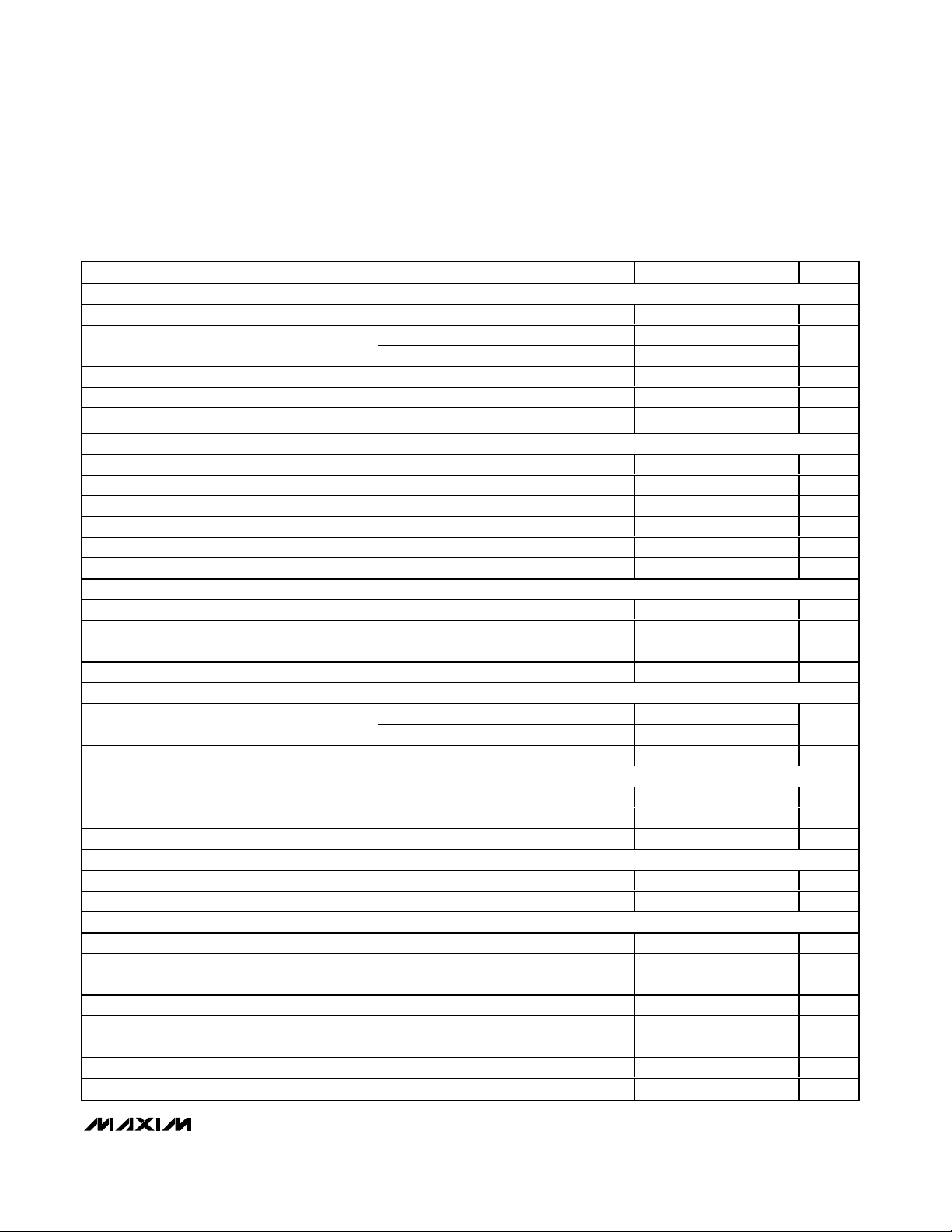
PARAMETER SYMBOL CONDITIONS
MIN
TYP
MAX
UNITS
REFERENCE
Output Voltage V
VREF
TA = +25°C, I
VREF
= 1mA
V
Line Regulation ∆V
LINE
12V < V
CC
< 25V, I
VREF
= 1mA 0.4 4 mV
Load Regulation ∆V
LOAD
1mA < I
VREF
< 20mA 6 25 mV
Total Output Variation V
REFT
1mA < I
VREF
< 20mA, 12V < V
CC
< 25V 4.9 5.1 V
Reference Output-Noise Voltage
V
NOISE
10Hz < f < 10kHz, TA = +25°C 50 µV
Reference Output Short Circuit I
S_SC
V
VREF =
0V -30
mA
OSCILLATOR
Initial Accuracy TA = +25°C 51 54 57 kHz
Voltage Stability 12V < VCC < 25V 0.2 0.5 %
Temp Stability -40°C < TA < +85°C 0.5 %
RT/CT Voltage Ramp (
P-P
)V
RAMP
1.7 V
RT/CT Voltage Ramp Valley
1.1 V
Discharge Current I
DIS
V
RT/CT
= 2V, TA = +25°C 7.9 8.3 8.7 mA
Frequency Range f
OSC
20
kHz
ERROR AMPLIFIER (MAX5070A/MAX5070B)
FB Input Voltage V
FB
FB shorted to COMP
2.5
V
FB Input Bias Current I
B(FB)
µA
Open-Loop Voltage Gain A
VOL
2V ≤ V
COMP
≤ 4V
dB
Unity-Gain Bandwidth f
GBW
1
MHz
Power-Supply Rejection Ratio PSRR 12V ≤ VCC ≤ 25V (Note 2) 60 80 dB
COMP Sink Current I
SINK
VFB = 2.7V, V
COMP
= 1.1V 2 6 mA
COMP Source Current I
SOURCE
VFB = 2.3V, V
COMP
= 5V
mA
COMP Output High Voltage V
COMPH
VFB = 2.3V, R
COMP
= 15kΩ to GND 5 5.8 V
COMP Output Low Voltage V
COMPL
VFB = 2.7V, R
COMP
= 15kΩ to VREF 0.1 1.1 V
CURRENT-SENSE AMPLIFIER
Gain A
CS
(Notes 3, 4)
3
V/V
MAX5070A/B (Note 3)
1
Maximum Current-Sense Signal V
CS_MAX
V
COMP
= 5V, MAX5071_
V
4.950 5.000 5.050
-100 -180
V
RAMP_VALLEY
2.465
-0.01 -0.1
100
-0.5 -1.2 -1.8
2.85
0.95
0.84 0.935 1.03
1000
2.535
3.26
1.05
Page 3
MAX5070/MAX5071
High-Performance, Single-Ended, Current-Mode
PWM Controllers
_______________________________________________________________________________________ 3
ELECTRICAL CHARACTERISTICS (continued)
(VCC= +15V, RT= 10kΩ, CT= 3.3nF, V
VREF
= OPEN, C
VREF
= 0.1µF, COMP = OPEN, VFB= 2V, CS = GND, TA= -40°C to +85°C,
unless otherwise noted.) (Note 1)
PARAMETER SYMBOL CONDITIONS
UNITS
Power-Supply Rejection Ratio PSRR 12V ≤ VCC ≤ 25V 70 dB
Input Bias Current I
CS
-1
µA
Delay From CS to OUT
50mV overdrive 60 ns
MOSFET DRIVER
OUT Low-Side On-Resistance
I
SINK
= 200mA 4.5 10 Ω
OUT High-Side On-Resistance
I
SOURCE
= 100mA 3.5 7 Ω
I
SOURCE
(Peak) I
SOURCE
C
OUT
= 10nF 2 A
I
SINK
(Peak) I
SINK
C
OUT
= 10nF 1 A
Rise Time t
r
C
OUT
= 1nF 15 ns
Fall Time t
f
C
OUT
= 1nF 22 ns
UNDERVOLTAGE LOCKOUT/STARTUP
Startup Voltage Threshold
16
V
Minimum Operating Voltage After
Turn-On
V
CC_MIN
9.2 10
V
Undervoltage-Lockout Hysteresis
6V
PWM
MAX5070A/MAX5071A
96
Maximum Duty Cycle D
MAX
MAX5070B/MAX5071B/MAX5071C 48
50
%
Minimum Duty Cycle D
MIN
0%
SUPPLY CURRENT
Startup Supply Current I
START
32 65 µA
Operating Supply Current I
CC
VFB = VCS = 0V 3 5 mA
Zener Bias Voltage at V
CC
V
Z
ICC = 25mA 24
V
THERMAL SHUTDOWN
Thermal Shutdown T
SHDN
°C
Thermal-Shutdown Hysteresis T
HYST
30 °C
SYNCHRONIZATION (MAX5071A/MAX5071B only) (Note 5)
SYNC Frequency Range f
SYNC
20
kHz
SYNC Clock Input High
Threshold
V
SYNCINH
3.5 V
SYNC Clock Input Low Threshold
V
SYNCINL
0.8 V
SYNC Clock Input Minimum
Pulse Width
ns
SYNC Clock Output High Level V
SYNCOH
1mA external pulldown 4.0 4.7 V
SYNC Clock Output Low Level V
SYNCOL
R
SYNC
= 5kΩ 0 0.1 V
SYNC Leakage Current I
SYNC
V
SYNC
= 0V
0.1 µA
MIN TYP MAX
t
CS_DELAY
V
RDS_ONL
V
RDS_ONH
V
CC_START
UVLO
HYST
15.2
94.5
49.8
26.5
+150
t
PW_SYNCIN
200
0.01
-2.5
16.8
10.8
97.5
1000
Page 4
MAX5070/MAX5071
High-Performance, Single-Ended, Current-Mode
PWM Controllers
4 _______________________________________________________________________________________
ELECTRICAL CHARACTERISTICS (continued)
(VCC= +15V, RT= 10kΩ, CT= 3.3nF, V
VREF
= OPEN, C
VREF
= 0.1µF, COMP = OPEN, VFB= 2V, CS = GND, TA= -40°C to +85°C,
unless otherwise noted.) (Note 1)
PARAMETER SYMBOL CONDITIONS
UNITS
ADV_CLK (MAX5071C only)
ADV_CLK High Voltage
I
ADV_CLK
= 10mA source 2.4 3 V
ADV_CLK Low Voltage
I
ADV_CLK
= 10mA sink 0.4 V
ADV_CLK Output Pulse Width t
PULSE
85 ns
ADV_CLK Rising Edge to OUT
Rising Edge
t
ADV_CLK
ns
ADV_CLK Source and Sink
Current
I
ADV_CLK
10 mA
ELECTRICAL CHARACTERISTICS
(VCC= +15V, RT= 10kΩ, CT= 3.3nF, V
VREF
= OPEN, C
VREF
= 0.1µF, COMP = OPEN, VFB= 2V, CS = GND, TA= -40°C to +125°C,
unless otherwise noted.) (Note 1)
PARAMETER SYMBOL CONDITIONS
MIN
TYP
MAX
UNITS
REFERENCE
Output Voltage V
VREF
TA = +25°C, I
VREF
= 1mA
V
Line Regulation ∆V
LINE
12V < V
CC
< 25V, I
VREF
= 1mA 0.4 4 mV
Load Regulation ∆V
LOAD
1mA < I
VREF
< 20mA 6 25 mV
Total Output Variation V
REFT
1mA < I
VREF
< 20mA, 12V < V
CC
< 25V 4.9 5.1 V
Reference Output Noise Voltage
V
NOISE
10Hz < f < 10kHz, TA = +25°C 50 µV
Reference Output Short Circuit I
S_SC
V
VREF
= 0V -30
mA
OSCILLATOR
Initial Accuracy TA = +25°C 51 54 57 kHz
Voltage Stability 12V < VCC < 25V 0.2 0.5 %
Temp Stability -40°C < TA < +125°C 1 %
RT/CT Voltage Ramp (
P-P
)V
RAMP
1.7 V
RT/CT Voltage Ramp Valley
1.1 V
Discharge Current I
DIS
V
RT/CT
= 2V, TA = +25°C 7.9 8.3 8.7 mA
Frequency Range f
OSC
20
kHz
ERROR AMPLIFIER (MAX5070A/MAX5070B)
FB Input Voltage V
FB
FB shorted to COMP
2.5
V
FB Input Bias Current I
B(FB)
µA
Open-Loop Voltage Gain A
VOL
2V ≤ V
COMP
≤ 4V
dB
Unity-Gain Bandwidth f
GBW
1
MHz
Power-Supply Rejection Ratio PSRR 12V ≤ VCC ≤ 25V (Note 2) 60 80 dB
COMP Sink Current I
SINK
V
FB
= 2.7V, V
COMP
= 1.1V 2 6 mA
COMP Source Current I
SOURCE
V
FB
= 2.3V, V
COMP
= 5V
mA
COMP Output High Voltage V
COMPH
V
FB
= 2.3V, R
COMP
=15kΩ to GND 5 5.8 V
COMP Output Low Voltage V
COMPL
V
FB
= 2.7V, R
COMP
= 15kΩ to VREF 0.1 1.1 V
V
ADV_CLKH
V
ADV_CLKL
MIN TYP MAX
110
4.950 5.000 5.050
-100 -180
V
RAMP_VALLEY
2.465
-0.01 -0.1
100
-0.5 -1.2 -1.8
1000
2.535
Page 5
MAX5070/MAX5071
High-Performance, Single-Ended, Current-Mode
PWM Controllers
_______________________________________________________________________________________ 5
ELECTRICAL CHARACTERISTICS (continued)
(VCC= +15V, RT= 10kΩ, CT= 3.3nF, V
VREF
= OPEN, C
VREF
= 0.1µF, COMP = OPEN, VFB= 2V, CS = GND, TA= -40°C to +125°C,
unless otherwise noted.) (Note 1)
PARAMETER SYMBOL CONDITIONS
UNITS
CURRENT-SENSE AMPLIFIER
Gain A
CS
(Notes 3, 4)
3
V/V
MAX5070A/B (Note 3)
1
Maximum Current-Sense Signal V
CS_MAX
V
COMP
= 5V, MAX5071_
V
Power-Supply Rejection Ratio PSRR 12V ≤ VCC ≤ 25V 70 dB
Input Bias Current I
CS
-1
µA
Delay From CS to OUT
50mV overdrive 60 ns
MOSFET DRIVER
OUT Low-Side On-Resistance
I
SINK
= 200mA 4.5 12 Ω
OUT High-Side On-Resistance
I
SOURCE
= 100mA 3.5 9 Ω
I
SOURCE
(Peak) I
SOURCE
C
OUT
= 10nF 2 A
I
SINK
(Peak) I
SINK
C
OUT
= 10nF 1 A
Rise Time t
r
C
OUT
= 1nF 15 ns
Fall Time t
f
C
OUT
= 1nF 22 ns
UNDERVOLTAGE LOCKOUT/STARTUP
Startup Voltage Threshold
16
V
Minimum Operating Voltage After
Turn-On
V
CC_MIN
9.2 10
V
Undervoltage-Lockout Hysteresis
6V
PWM
MAX5070A/MAX5071A
96
Maximum Duty Cycle D
MAX
MAX5070B/MAX5071B/MAX5071C 48
50
%
Minimum Duty Cycle D
MIN
0%
SUPPLY CURRENT
Startup Supply Current I
START
32 65 µA
Operating Supply Current I
CC
VFB = VCS = 0V 3 5 mA
Zener Bias Voltage at V
CC
V
Z
ICC = 25mA 24
V
THERMAL SHUTDOWN
Thermal Shutdown T
SHDN
°C
Thermal-Shutdown Hysteresis T
HYST
30 °C
SYNCHRONIZATION (MAX5071A/MAX5071B only, Note 5)
SYNC Frequency Range f
SYNC
20
kHz
SYNC Clock Input High
Threshold
3.5 V
SYNC Clock Input Low Threshold
V
SYNCINL
0.8 V
SYNC Clock Input Minimum
Pulse Width
ns
SYNC Clock Output High Level V
SYNCOH
1mA external pulldown 4.0 4.7 V
SYNC Clock Output Low Level V
SYNCOL
R
SYNC
= 5kΩ 0 0.1 V
MIN TYP MAX
2.85
0.95
0.84 0.935 1.03
t
CS_DELAY
V
RDS_ONL
V
RDS_ONH
V
CC_START
UVLO
HYST
15.2
94.5
49.8
26.5
+150
V
SYNCINH
t
PW_SYNCIN
200
3.26
1.05
-2.5
16.8
10.8
97.5
1000
Page 6
MAX5070/MAX5071
High-Performance, Single-Ended, Current-Mode
PWM Controllers
6 _______________________________________________________________________________________
ELECTRICAL CHARACTERISTICS (continued)
(VCC= +15V, RT= 10kΩ, CT= 3.3nF, V
VREF
= OPEN, C
VREF
= 0.1µF, COMP = OPEN, VFB= 2V, CS = GND, TA= -40°C to +125°C,
unless otherwise noted.) (Note 1)
PARAMETER SYMBOL CONDITIONS
UNITS
SYNC Leakage Current I
SYNC
V
SYNC
= 0V
0.1 µA
ADV_CLK (MAX5071C only)
ADV_CLK High Voltage
I
ADV_CLK
= 10mA source 2.4 3 V
ADV_CLK Low Voltage
I
ADV_CLK
= 10mA sink 0.4 V
ADV_CLK Output Pulse Width t
PULSE
85 ns
ADV_CLK Rising Edge to OUT
Rising Edge
t
ADV_CLK
ns
ADV_CLK Source and Sink
Current
I
ADV_CLK
10 mA
Note 1:All devices are 100% tested at +25°C. All limits over temperature are guaranteed by design, not production tested.
Note 2: Guaranteed by design, not production tested.
Note 3: Parameter measured at trip point of latch with V
FB
= 0V (MAX5070A/MAX5070B only).
Note 4: Gain is defined as A = ∆V
COMP
/∆VCS, 0 ≤ VCS≤ 0.8V.
Note 5: Output Frequency equals oscillator frequency for MAX5070A/MAX5071A. Output frequency is one-half oscillator frequency
for MAX5070B/MAX5071B/MAX5071C.
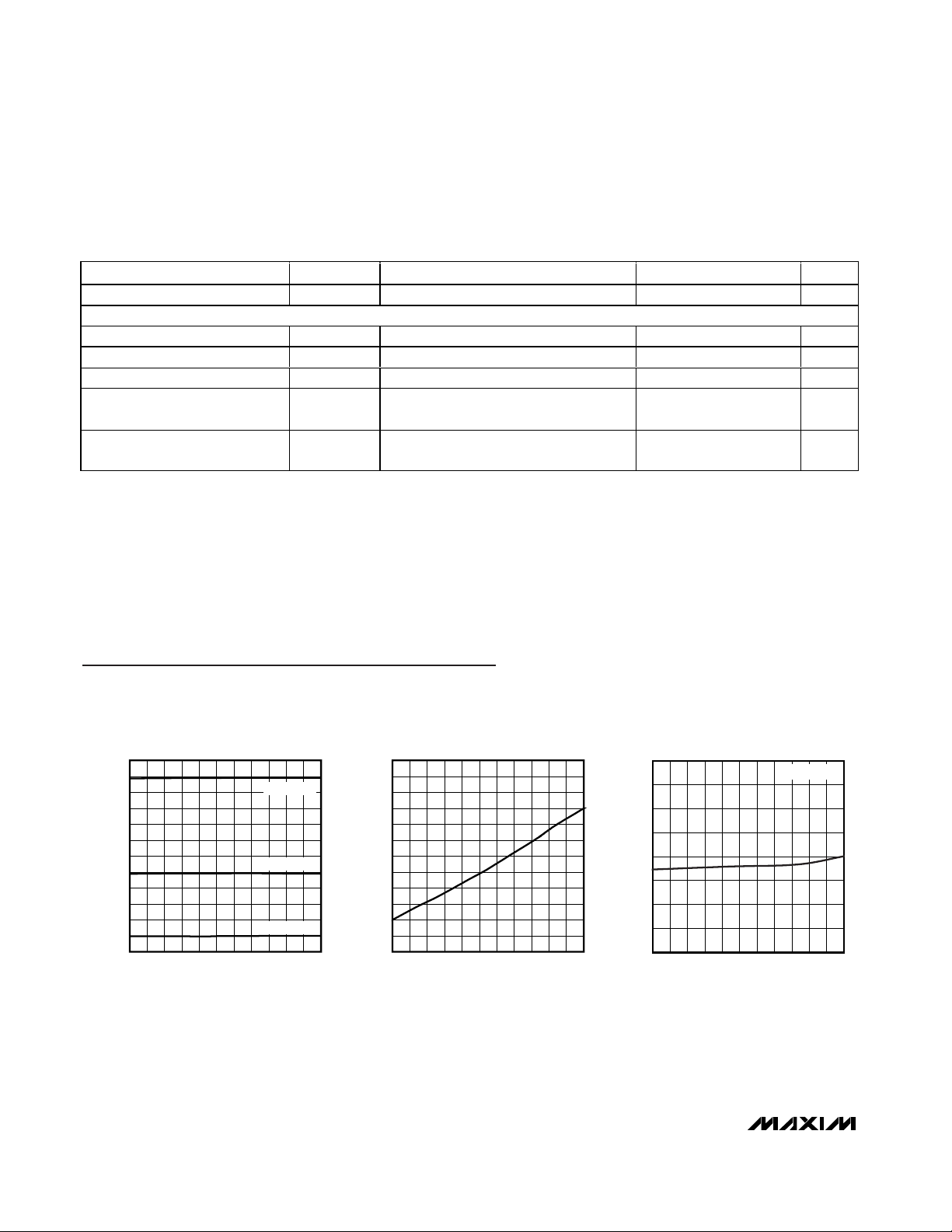
BOOTSTRAP UVLO vs. TEMPERATURE
MAX5070 toc01
TEMPERATURE (°C)
V
CC
(V)
1109565 80-10 5 20 35 50-25
6
7
8
9
10
11
12
13
14
15
16
17
5
-40 125
HYSTERESIS
VCC FALLING
VCC RISING
STARTUP CURRENT vs. TEMPERATURE
MAX5070 toc02
TEMPERATURE (°C)
STARTUP CURRENT (µA)
1109565 80-10 5 20 35 50-25
29
30
31
32
33
34
35
36
37
38
39
40
28
-40 125
2.0
2.5
5.5
3.5
3.0
4.0
4.5
5.0
6.0
-40 -10 5 20-25 35 50 9580 11065 125
OPERATING SUPPLY CURRENT (ICC)
vs. TEMPERATURE AFTER STARTUP
(f
OSC
= fSW = 250kHz)
MAX5070 toc03
TEMPERATURE (°C)
SUPPLY CURRENT (mA)
CT = 100pF
Typical Operating Characteristics
(VCC= 15V, TA = +25°C, unless otherwise noted.)
V
ADV_CLKH
V
ADV_CLKL
MIN TYP MAX
0.01
110
Page 7
MAX5070/MAX5071
High-Performance, Single-Ended, Current-Mode
PWM Controllers
_______________________________________________________________________________________ 7
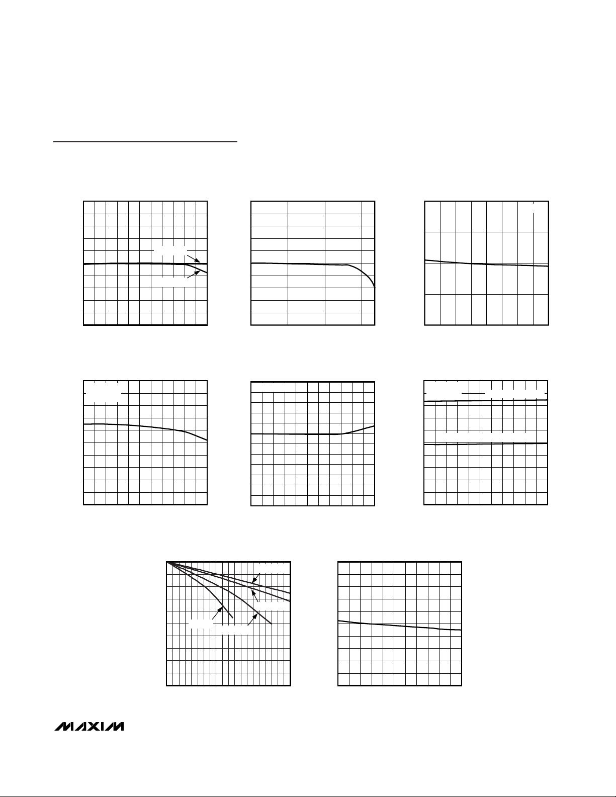
REFERENCE VOLTAGE (VREF)
vs. TEMPERATURE
MAX5070 toc04
TEMPERATURE (°C)
V
VREF
(V)
1109565 80-10 5 20 35 50-25-40 125
4.6
4.7
4.8
4.9
5.0
5.1
5.2
5.3
5.4
5.5
4.5
I
REF
= 20mA
I
REF
= 1mA
REFERENCE VOLTAGE (VREF)
vs. REFERENCE LOAD CURRENT
MAX5070 toc05
I
REF
(mA)
V
VREF
(V)
453015
4.80
4.85
4.90
4.95
5.00
5.05
5.10
5.15
5.20
5.25
4.75
0
REFERENCE VOLTAGE (VREF)
vs. V
CC
VOLTAGE
MAX5070 toc06
VCC (V)
V
VREF
(V)
24222018161412
4.995
5.000
5.005
5.010
4.990
10 26
I
REF
= 1mA
OSCILLATOR FREQUENCY (f
OSC
)
vs. TEMPERATURE
MAX5070 toc07
TEMPERATURE (°C)
OSCILLATOR FREQUENCY (kHz)
1109565 80-10 5 20 35 50-25-40 125
460
470
480
490
500
510
520
530
540
550
450
RT = 3.01kΩ
C
T
= 1nF
OSCILLATOR RT/CT DISCHARGE CURRENT
vs. TEMPERATURE
MAX5070 toc08
TEMPERATURE (°C)
R
T
/C
T
DISCHARGE CURRENT (mA)
1109565 80-10 5 20 35 50-25
8.05
8.10
8.15
8.20
8.25
8.30
8.35
8.40
8.45
8.50
8.55
8.60
8.00
-40 125
V
RT/CT
= 2V
MAXIMUM DUTY CYCLE
vs. TEMPERATURE
MAX5070 toc09
TEMPERATURE (°C)
DUTY CYCLE (%)
1109565 80-10 5 20 35 50-25-40 125
10
20
30
40
50
60
70
80
90
100
0
RT = 3.01kΩ
C
T
= 1nF
MAX5070A/MAX5071A
MAX5070B/MAX5071B/MAX5071C
MAX5070A/MAX5071A
MAXIMUM DUTY CYCLE vs. FREQUENCY
MAX5070 toc10
OSCILLATOR FREQUENCY (kHz)
DUTY CYCLE (%)
1200 1600
30
20
10
40
50
60
70
80
90
100
0
0400 800 2000
CT = 100pF
CT = 1nF
CT = 560pF
CT = 220pF
CURRENT-SENSE (CS) TRIP THRESHOLD
vs. TEMPERATURE
MAX5070 toc11
TEMPERATURE (°C)
CS THRESHOLD (V)
1109565 80-10 5 20 35 50-25-40 125
0.92
0.94
0.96
0.98
1.00
1.02
1.04
1.06
1.08
1.10
0.90
Typical Operating Characteristics (continued)
(VCC= 15V, TA = +25°C, unless otherwise noted.)
Page 8

MAX5070/MAX5071
High-Performance, Single-Ended, Current-Mode
PWM Controllers
8 _______________________________________________________________________________________
Typical Operating Characteristics (continued)
(VCC= 15V, TA = +25°C, unless otherwise noted.)
TIMING RESISTANCE (RT)
vs. OSCILLATOR FREQUENCY
MAX5070 toc12
FREQUENCY (Hz)
R
T
RESISTANCE (kΩ)
1M100k
1
10
100
1000
0.1
10k 10M
CT = 10nF
C
T
= 4.7nF
C
T
= 3.3nF
C
T
= 2.2nF
CT = 1nF
C
T
= 560pF
C
T
= 220pF
C
T
= 100pF
OUT IMPEDANCE vs. TEMPERATURE
(R
DS_ON
PMOS DRIVER)
MAX5070 toc13
TEMPERATURE (°C)
R
DS_ON
(Ω)
1109565 80-10 5 20 35 50-25
2.2
2.4
2.6
2.8
3.0
3.2
3.4
3.6
3.8
4.0
4.2
4.4
4.6
4.8
5.0
2.0
-40 125
I
SOURCE
= 100mA
OUT IMPEDANCE vs. TEMPERATURE
(R
DS_ON
NMOS DRIVER)
MAX5070 toc14
TEMPERATURE (°C)
R
DS_ON
(Ω)
1109565 80-10 5 20 35 50-25
3.5
4.0
4.5
5.0
5.5
6.0
6.5
7.0
7.5
8.0
8.5
9.0
3.0
-40 125
I
SINK
= 200mA
PROPAGATION DELAY FROM CURRENT-LIMIT
COMPARATOR TO OUT vs. TEMPERATURE
MAX5070 toc15
TEMPERATURE (°C)
PROPAGATION DELAY (ns)
1109565 80-10 5 20 35 50-25-40 125
10
20
30
40
50
60
70
80
90
100
0
ERROR-AMPLIFIER OPEN-LOOP GAIN
AND PHASE vs. FREQUENCY
MAX5070 toc16
FREQUENCY (Hz)
GAIN (dB)
1M100k1k 10k10 1001
0
20
40
60
80
100
120
140
-20
0.01
100M
10M
-165
-140
-115
-90
-65
-40
-15
10
-190
PHASE
GAIN
PHASE (DEGREES)
COMP VOLTAGE LEVEL TO TURN OFF DEVICE
vs. TEMPERATURE
MAX5070 toc17
TEMPERATURE (°C)
V
COMP
(V)
1109565 80-10 5 20 35 50-25-40 125
1.6
1.7
1.8
1.9
2.0
2.1
2.2
2.3
2.4
2.5
1.5
10V < VCC < 18V
ADV_CLK RISING EDGE TO OUT RISING EDGE
PROPAGATION DELAY vs. TEMPERATURE
MAX5070 toc18
TEMPERATURE (°C)
PROPAGATION DELAY (ns)
1109565 80-10 5 20 35 50-25
92
94
96
98
100
102
104
106
108
110
112
114
90
-40 125
MAX5071C
ADV_CLK AND OUT WAVEFORMS
MAX5070 toc19
VCC = 15V
MAX5071C
OUT
10V/div
10kΩ LOAD
ADV_CLK
5V/div
20ns/div
Page 9

MAX5070/MAX5071
High-Performance, Single-Ended, Current-Mode
PWM Controllers
_______________________________________________________________________________________ 9
OUT SOURCE AND SINK CURRENTS
MAX5070 toc20
VCC = 15V
I
OUT
2A/div
V
OUT
10V/div
20Ons/div
C
OUT
= 10nF
2
4
3
5
8
9
7
6
10
20 220 320 420 520120 620 720 820 920 1020
SUPPLY CURRENT (ICC)
vs. OSCILLATOR FREQUENCY (C
T
= 100pF)
MAX5070 toc21
FREQUENCY (kHz)
SUPPLY CURRENT (mA)
TA = +125°C
TA = +85°C
TA = +25°C
TA = -40°C
MAX5070A/MAX5071A
MAXIMUM DUTY CYCLE vs. R
T
MAX5070 toc22
RT (Ω)
DUTY CYCLE (%)
10k1k
30
40
50
60
70
80
90
100
20
100 100k
CT = 1nF
C
T
= 560pF
C
T
= 220pF
C
T
= 100pF
Typical Operating Characteristics (continued)
(VCC= 15V, TA = +25°C, unless otherwise noted.)
Pin Descriptions
PIN NAME FUNCTION
1 COMP Error-Amplifier Output. COMP can be used for soft-start.
2FBError-Amplifier Inverting Input
3CS
Input to the PWM Comparator and Overcurrent Protection Comparator. The current-sense signal is
compared to a signal proportional to the error-amplifier output voltage.
4R
T/CT
Timing Resistor and Capacitor Connection. A resistor RT from RT/CT to VREF and capacitor CT from
R
T/CT
to GND set the oscillator frequency.
5 GND
Power-Supply Ground. Place the V
CC
and VREF bypass capacitors close to the IC to minimize
ground loops.
6 OUT MOSFET Driver Output. OUT connects to the gate of the external n-channel MOSFET.
7V
CC
Power-Supply Input for MAX5070. Bypass VCC to GND with a 0.1µF ceramic capacitor or a parallel
combination of a 0.1µF and a higher value ceramic capacitor.
8 VREF
5V Reference Output. Bypass VREF to GND with a 0.1µF ceramic capacitor or a parallel combination
of a 0.1µF and a higher value ceramic capacitor.
MAX5070A/MAX5070B
Page 10

MAX5070/MAX5071
High-Performance, Single-Ended, Current-Mode
PWM Controllers
10 ______________________________________________________________________________________
Pin Descriptions (continued)
PIN
MAX5071A/
MAX5071B
NAME FUNCTION
11COMP
COMP is level-shifted and connected to the inverting input of the PWM comparator. Pull
up COMP to VREF through a resistor and connect an optocoupler from COMP to GND for
proper operation.
2—SYNC
Bidirectional Synchronization Input. When synchronizing with other
MAX5071A/MAX5071Bs, the higher frequency part synchronizes all other devices.
—2
ADV_CLK is an 85ns clock output pulse preceding the rising edge of OUT (see Figure 4).
Use the pulse to drive the secondary-side synchronous rectifiers through a pulse
transformer or an optocoupler (see Figure 8).
33CS
Input to the PWM Comparator and Overcurrent Protection Comparator. The currentsense signal is compared to the voltage at COMP.
44R
T/CT
Timing Resistor and Capacitor Connection. A resistor RT from RT/CT to VREF and
capacitor C
T
from RT/CT to GND set the oscillator frequency.
55GND
Power-Supply Ground. Place the V
CC
and VREF bypass capacitors close to the IC to
minimize ground loops.
66OUT MOSFET Driver Output. OUT connects to the gate of the external n-channel MOSFET.
77V
CC
Power-Supply Input for MAX5071. Bypass VCC to GND with a 0.1µF ceramic capacitor or
a parallel combination of a 0.1µF and a higher value ceramic capacitor.
88V
REF
5V Reference Output. Bypass VREF to GND with a 0.1µF ceramic capacitor or a parallel
combination of a 0.1µF and a higher value ceramic capacitor.
MAX5071A/MAX5071B/MAX5071C
MAX5071C
ADV_CLK
Page 11

Detailed Description
The MAX5070/MAX5071 current-mode PWM controllers
are designed for use as the control and regulation core of
flyback or forward topology switching power supplies.
These devices incorporate an integrated low-side driver,
adjustable oscillator, error amplifier (MAX5070A/
MAX5070B only), current-sense amplifier, 5V reference,
and external synchronization capability (MAX5071A/
MAX5071B only). An internal +26.5V current-limited V
CC
clamp prevents overvoltage during startup.
Five different versions of the MAX5070/MAX5071 are
available. The MAX5070A/MAX5070B are the standard
versions with a feedback input (FB) and internal error
amplifier. The MAX5071A/MAX5071B include bidirectional synchronization (SYNC). This enables multiple
MAX5071A/MAX5071Bs to be connected and synchronized to the device with the highest frequency. The
MAX5071C includes an ADV_CLK output, which precedes the MAX5071C’s drive output (OUT) by 110ns.
Figures 1, 2, and 3 show the internal functional diagrams
of the MAX5070A/MAX5070B, MAX5071A/MAX5071B,
and MAX5071C, respectively. The MAX5070A/
MAX5071A are capable of 100% maximum duty cycle.
The MAX5070B/MAX5071B/MAX5071C are designed to
limit the maximum duty cycle to 50%.
MAX5070/MAX5071
High-Performance, Single-Ended, Current-Mode
PWM Controllers
______________________________________________________________________________________ 11
UVLO
REFERENCE
2.5V
PREREGULATOR
5V
VOLTAGE-
DIVIDER
THERMAL
SHUTDOWN
EN-REF
BG
SNS
V
DD
5V REGULATOR
VOLTAGE-
DIVIDER
8
7
26.5V
V
CC
VREF
2.5V
VP
REG_OK
DELAY
SRQ
OSC Q
4
RT/C
T
6
OUT
ILIM
CPWM
1V
EN-DRV-BAR
R
2R
VEA
3
5
2
1
CS
GND
FB
COMP
CLK
MAX5070A/MAX5070B
VP
2.5V
16V/10V
100% MAX DUTY CYCLE (MAX5070A)
50% MAX DUTY CYCLE (MAX5070B)
Figure 1. MAX5070A/MAX5070B Functional Diagram
Page 12

MAX5070/MAX5071
Current-Mode Control Loop
The advantages of current-mode control over voltagemode control are twofold. First, there is the feed-forward
characteristic brought on by the controller’s ability to
adjust for variations in the input voltage on a cycle-bycycle basis. Secondly, the stability requirements of the
current-mode controller are reduced to that of a singlepole system unlike the double pole in the voltage-mode
control scheme.
The MAX5070/MAX5071 use a current-mode control loop
where the output of the error amplifier is compared to the
current-sense voltage (VCS). When the current-sense signal is lower than the noninverting input of the PWM comparator, the output of the CPWM comparator is low and
the switch is turned on at each clock pulse. When the
current-sense signal is higher than the inverting input of
the CPWM, the output of the CPWM comparator is high
and the switch is turned off.
High-Performance, Single-Ended, Current-Mode
PWM Controllers
12 ______________________________________________________________________________________
UVLO
REFERENCE
2.5V
PREREGULATOR
5V
VOLTAGE-
DIVIDER
THERMAL
SHUTDOWN
EN-REF
BG
SNS
V
DD
5V REGULATOR
VOLTAGE-
DIVIDER
8
7
26.5V
V
CC
VREF
2.5V
VP
REG_OK
DELAY
SRQ
OSC Q
4
RT/C
T
6
OUT
ILIM
CPWM
1V
EN-DRV-BAR
R
2R
3
5
1
2
CS
GND
COMP
SYNC
CLK
MAX5071A/MAX5071B
VP
2.5V
1V
BIDIRECTIONAL
SYNC
100% MAX DUTY CYCLE (MAX5071A)
50% MAX DUTY CYCLE (MAX5071B)
16V/10V
Figure 2. MAX5071A/MAX5071B Functional Diagram
Page 13

VCCand Startup
In normal operation, VCCis derived from a tertiary winding of the transformer. However, at startup there is no
energy delivered through the transformer, thus a resistor
must be connected from V
CC
to the input power source
(see RSTand CSTin Figures 5 to 8). During startup, C
ST
charges up through RST. The 5V reference generator,
comparator, error amplifier, oscillator, and drive circuit
remain off during UVLO to reduce startup current below
65µA. When VCCreaches the undervoltage-lockout
threshold of 16V, the output driver begins to switch and
the tertiary winding will supply power to V
CC
. VCChas an
internal 26.5V current-limited clamp at its input to protect
the device from overvoltage during startup.
Size the startup resistor, R
ST
, to supply both the maxi-
mum startup bias (I
START
) of the device (65µA max)
and the charging current for CST. The startup capacitor
CSTmust charge to 16V within the desired time period
tST(for example, 500ms). The size of the startup
capacitor depends on:
1) IC operating supply current at a programmed oscilla-
tor frequency (f
OSC
).
2) The time required for the bias voltage, derived from
a bias winding, to go from 0 to 11V.
3) The MOSFET total gate charge.
4) The operating frequency of the converter (fSW).
MAX5070/MAX5071
High-Performance, Single-Ended, Current-Mode
PWM Controllers
______________________________________________________________________________________ 13
UVLO
REFERENCE
2.5V
PREREGULATOR
5V
VOLTAGE-
DIVIDER
THERMAL
SHUTDOWN
EN-REF
BG
SNS
V
DD
5V REGULATOR
VOLTAGE-
DIVIDER
8
7
26.5V
V
CC
VREF
2.5V
VP
REG_OK
DELAY
SRQ
OSC Q
4
RT/C
T
6
OUT
ILIM
CPWM
1V
EN-DRV-BAR
R
2R
3
5
1
2
CS
GND
COMP
ADV_CLK
CLK
MAX5071C
VP
2.5V
1V
50% MAX DUTY CYCLE
16V/10V
Figure 3. MAX5071C Functional Diagram
Page 14

MAX5070/MAX5071
To calculate the capacitance required, use the following
formula:
where:
IG= QGf
SW
ICCis the MAX5070/MAX5071s’ maximum internal supply current after startup (see the Typical Operating
Characteristics to find the IINat a given f
OSC
). QG is the
total gate charge for the MOSFET, fSWis the converter
switching frequency, V
HYST
is the bootstrap UVLO hysteresis (6V), and tSSis the soft-start time, which is set
by external circuitry.
Size the resistor R
ST
according to the desired startup
time period, t
ST
, for the calculated CST. Use the following equations to calculate the average charging current
(I
CST
) and the startup resistor (RST).
Where V
INMIN
is the minimum input supply voltage for
the application (36V for telecom), V
SUVR
is the boot-
strap UVLO wake-up level (16V), and I
START
is the V
IN
supply current at startup (65µA, max). Choose a higher
value for RSTthan the one calculated above if longer
startup times can be tolerated in order to minimize
power loss in RST.
The above startup method is applicable to circuits where
the tertiary winding has the same phase as the output
windings. Thus, the voltage on the tertiary winding at any
given time is proportional to the output voltage and goes
through the same soft-start period as the output voltage.
The minimum discharge time of CSTfrom 16V to 10V
must be greater than the soft-start time (tSS).
Undervoltage Lockout (UVLO)
The minimum turn-on supply voltage for the
MAX5070/MAX5071 is 16V. Once VCCreaches 16V, the
reference powers up. There is 6V of hysteresis from the
minimum turn-on voltage to the UVLO threshold. Once
VCCreaches 16V, the MAX5070/MAX5071 will operate
with V
CC
down to 10V. Once VCCgoes below 10V the
device is in UVLO. When in UVLO, the quiescent supply current into VCCfalls back to 37µA (typ), and OUT
and VREF are pulled low.
MOSFET Driver
OUT drives an external n-channel MOSFET and swings
from GND to VCC. Ensure that VCCremains below the
absolute maximum VGSrating of the external MOSFET.
OUT is a push-pull output with the on-resistance of the
PMOS typically 3.5Ω and the on-resistance of the NMOS
typically 4.5Ω. The driver can source 2A typically and
sink 1A typically. This allows for the MAX5070/MAX5071
to quickly turn on and off high gate-charge MOSFETs.
Bypass VCCwith one or more 0.1µF ceramic capacitors
to GND, placed close to the MAX5070/MAX5071. The
average current sourced to drive the external MOSFET
depends on the total gate charge (QG) and operating
frequency of the converter. The power dissipation in the
MAX5070/MAX5071 is a function of the average output
drive current (I
DRIVE
). Use the following equation to cal-
culate the power dissipation in the device due to I
DRIVE
:
I
DRIVE
= QGx f
SW
PD = (I
DRIVE
+ ICC) x V
CC
where ICCis the operating supply current. See the
Typical Operating Characteristics for the operating
supply current at a given frequency.
Error Amplifier (MAX5070A/MAX5070B)
The MAX5070 includes an internal error amplifier. The
inverting input is at FB and the noninverting input is internally connected to a 2.5V reference. The internal error
amplifier is useful for nonisolated converter design (see
Figure 6) and isolated design with primary-side regulation
through a bias winding (see Figure 5). In the case of a
nonisolated power supply, the output voltage will be:
where R1 and R2 are from Figure 6.
V
R
R
V
OUT
=+
×1
1
2
25.
R
V
V
II
ST
INMIN
SUVR
CST START
≅
−
+
2
I
VC
t
CST
SUVR ST
ST
=
×
C
II
VV
R
t
V
ST
CC G
INMIN
ST
SS
HYST
=
+ −
−
()
13
High-Performance, Single-Ended, Current-Mode
PWM Controllers
14 ______________________________________________________________________________________
Page 15

MAX5071A/MAX5071B/MAX5071C
Feedback
The MAX5071A/MAX5071B/MAX5071C are designed to
be used with either an external error amplifier when
designed into a nonisolated converter or an error amplifier and optocoupler when designed into an isolated
power supply. The COMP input is level-shifted and
connected to the inverting terminal of the PWM comparator (CPWM). Connect the COMP pin to the output
of the external error amplifier for nonisolated design.
Pull COMP high externally to at least 5V (or VREF) and
connect the optocoupler transistor as shown in Figures
7 and 8. COMP can be used for soft-start and also as a
shutdown. See the Typical Operating Characteristics to
find the turn-off COMP voltage at different temperatures. If the maximum external COMP voltage is below
4.9V, it may reduce the PWM current-limit threshold
below 1V. Use the following equation to calculate minimum COMP voltage (V
COMP
) required for a guaranteed
peak primary current (I
P-P
):
V
COMP
= (3 x I
P-P
x RCS) + 1.95V
where RCSis a current-sense resistor.
Oscillator
The oscillator frequency is adjusted by adding an
external capacitor and resistor at RT/CT(see RTand C
T
in the Typical Application Circuits). RTis connected
from RT/CTto the 5V reference (VREF) and CTis connected from RT/CTto GND. VREF charges CTthrough
RTuntil its voltage reaches 2.8V. CTthen discharges
through an 8.3mA internal current sink until CT’s voltage
reaches 1.1V, at which time CTis allowed to charge
through RTagain. The oscillator’s period will be the
sum of the charge and discharge times of CT. Calculate
the charge time as:
tC= 0.57 x RTx C
T
The discharge time is then:
The oscillator frequency will then be:
For the MAX5070A/MAX5071A, the converter output
switching frequency (fSW) is the same as the oscillator
frequency (f
OSC
). For the MAX5070B/MAX5071B/
MAX5071C, the output switching frequency is 1/2 the
oscillator frequency.
Reference Output
VREF is a 5V reference output that can source 20mA.
Bypass VREF to GND with a 0.1µF capacitor.
Current Limit
The MAX5070/MAX5071 include a fast current-limit comparator to terminate the ON cycle during an overload or a
fault condition. The current-sense resistor (RCS), connected between the source of the MOSFET and GND, sets
the current limit. The CS input has a voltage trip level
(VCS) of 1V. Use the following equation to calculate RCS:
I
P-P
is the peak current in the primary that flows through
the MOSFET. When the voltage produced by this current
(through the current-sense resistor) exceeds the currentlimit comparator threshold, the MOSFET driver (OUT) will
turn the switch off within 60ns. In most cases, a small RC
filter is required to filter out the leading-edge spike on the
sense waveform. Set the time constant of the RC filter at
50ns. Use a current transformer to limit the losses in the
current-sense resistor and achieve higher efficiency
especially at low input-voltage operation.
Synchronization (MAX5071A/MAX5071B)
SYNC
SYNC is a bidirectional input/output that outputs a synchronizing pulse and accepts a synchronizing pulse
from other MAX5071A/MAX5071Bs (see Figures 7 and
9). As an output, SYNC is an open-drain p-channel
MOSFET driven from the internal oscillator and requires
an external pulldown resistor (R
SYNC
) from between
500Ω and 5kΩ. As an input, SYNC accepts the output
pulses from other MAX5071A/MAX5071Bs.
Synchronize multiple MAX5071A/MAX5071Bs by connecting their SYNC pins together. All devices connected
together will synchronize to the one operating at the
highest frequency. The rising edge of SYNC will precede
the rising edge of OUT by approximately the discharge
time (t
D
) of the oscillator (see the Oscillator section). The
pulse width of the SYNC output is equal to the time
required to discharge the stray capacitance at SYNC
through R
SYNC
plus the CTdischarge time tD. Adjust
RT/CTsuch that the minimum discharge time tDis 200ns.
R
V
I
CS
CS
PP
=
−
f
tt
OSC
CD
=
+
1
t
RC
R
D
TT
T
=
××
× − ×
10
488 18 10
3
3
..
MAX5070/MAX5071
High-Performance, Single-Ended, Current-Mode
PWM Controllers
______________________________________________________________________________________ 15
Page 16

MAX5070/MAX5071
Advance Clock Output (ADV_CLK) (MAX5071C)
ADV_CLK is an advanced pulse output provided to
facilitate the easy implementation of secondary-side
synchronous rectification using the MAX5071C. The
ADV_CLK pulse width is 85ns (typically) with its rising
edge leading the rising edge of OUT by 110ns. Use
this leading pulse to turn off the secondary-side synchronous-rectifier MOSFET (QS) before the voltage
appears on the secondary (see Figure 8). Turning off
the secondary-side synchronous MOSFET earlier
avoids the shorting of the secondary in the forward
converter. The ADV_CLK pulse can be propagated to
the secondary side using a pulse transformer or highspeed optocoupler. The 85ns pulse, with 3V drive voltage (10mA source), significantly reduces the
volt-second requirement of the pulse transformer and
the advanced pulse alleviates the need for a highspeed optocoupler.
Thermal Shutdown
When the MAX5070/MAX5071s’ die temperature goes
above +150°C, the thermal-shutdown circuitry will shut
down the 5V reference and pull OUT low.
High-Performance, Single-Ended, Current-Mode
PWM Controllers
16 ______________________________________________________________________________________
t
ADV_CLK
= 110ns
t
PULSE
= 85ns
OUT
ADV_CLK
R
T/CT
Figure 4. ADV_CLK
Typical Application Circuits
R
T
R1
R2
1
2
4
3
VREF
V
CC
GND
OUT
COMP
FB
R
T/CT
CS
8
7
5
6
MAX5070A
MAX5070B
C
T
R
ST
V
IN
C
ST
V
OUT
N
R
CS
Figure 5. MAX5070A/MAX5070B Typical Application Circuit (Isolated Flyback with Primary-Side Regulation)
Page 17

MAX5070/MAX5071
High-Performance, Single-Ended, Current-Mode
PWM Controllers
______________________________________________________________________________________ 17
Typical Application Circuits (continued)
R
T
R1
R2
1
2
4
3
VREF
V
CC
GND
OUT
COMP
FB
R
T/CT
CS
8
7
5
6
MAX5070A
MAX5070B
C
T
R
ST
V
IN
C
ST
R
CS
V
OUT
N
Figure 6. MAX5070A/MAX5070B Typical Application Circuit (Non-Isolated Flyback)
R
T
1
2
4
3
VREF
V
CC
GND
OUT
COMP
SYNC
R
T/CT
CS
8
7
5
6
MAX5071A
MAX5071B
C
T
R
ST
V
IN
C
ST
V
OUT
SYNC
INPUT/OUTPUT
N
R
SYNC
R
CS
Figure 7. MAX5071A/MAX5071B Typical Application Circuit (Isolated Flyback)
Page 18

MAX5070/MAX5071
High-Performance, Single-Ended, Current-Mode
PWM Controllers
18 ______________________________________________________________________________________
Typical Application Circuits (continued)
MAX5071C
V
CC
GND
COMP
R
T/CT
VREF
CS
OUT
R
T
C
T
V
IN
ADV_CLK
C
ST
R
ST
0.5V/µs PULSE TRANSFORMER
MAX5078
V
D
QR
N
N
N
QS
V
OUT
V
D
R
CS
Figure 8. MAX5071C Typical Application Circuit (Isolated Forward with Secondary-Side Synchronous Rectification)
Page 19

MAX5070/MAX5071
High-Performance, Single-Ended, Current-Mode
PWM Controllers
______________________________________________________________________________________ 19
MAX5071A
MAX5071B
V
CC
GND
SYNC
R
T/CT
VREF
CS
OUT
R
T
C
T
V
IN
MAX5071A
MAX5071B
V
CC
GND
SYNC
R
T/CT
VREF
CS
OUT
R
T
C
T
V
IN
MAX5071A
MAX5071B
V
CC
GND
SYNC
R
T/CT
VREF
CS
OUT
R
T
C
T
V
IN
TO OTHER
MAX5071A/Bs
R
SYNC
NN N
Figure 9. Synchronization of MAX5071s
Page 20

MAX5070/MAX5071
High-Performance, Single-Ended, Current-Mode
PWM Controllers
20 ______________________________________________________________________________________
Chip Information
TRANSISTOR COUNT: 1987
PROCESS: BiCMOS
Ordering Information (continued)
PART TEMP RANGE
PIN-PACKAGE
MAX5071AASA*
8 SO
MAX5071AAUA*
8 µMAX
MAX5071BASA
8 SO
MAX5071BAUA
8 µMAX
MAX5071CASA
8 SO
MAX5071CAUA
8 µMAX
Pin Configurations (continued)
Selector Guide
PART
FEEDBACK/
MAXIMUM DUTY
CYCLE (%)
PIN-PACKAGE PIN COMPATIBLE
MAX5070AASA Feedback 100 8 SO UC2842/UCC2842
MAX5070AAUA Feedback 100 8 µMAX UC2842/UCC2842
MAX5070BASA Feedback 50 8 SO UC2844/UCC2844
MAX5070BAUA Feedback 50 8 µMAX UC2844/UCC2844
MAX5071AASA Sync. 100 8 SO —
MAX5071AAUA Sync. 100 8 µMAX —
MAX5071BASA Sync. 50 8 SO —
MAX5071BAUA Sync. 50 8 µMAX —
MAX5071CASA ADV_CLK 50 8 SO —
MAX5071CAUA ADV_CLK 50 8 µMAX —
*Future product—contact factory for availability.
ADVANCED CLOCK
TOP VIEW
1
COMP
2
SYNC
CS
T/CT
3
4
MAX5071A
MAX5071B
µMAX/SO
-40°C to +125°C
-40°C to +125°C
-40°C to +125°C
-40°C to +125°C
-40°C to +125°C
-40°C to +125°C
87VREF
V
CC
OUT
6
GNDR
5
COMP
ADV_CLK
T/CT
1
2
MAX5071C
3
CS
4
µMAX/SO
87VREF
V
CC
OUT
6
GNDR
5
Page 21

MAX5070/MAX5071
High-Performance, Single-Ended, Current-Mode
PWM Controllers
______________________________________________________________________________________ 21
Package Information
(The package drawing(s) in this data sheet may not reflect the most current specifications. For the latest package outline information
go to www.maxim-ic.com/packages
.)
SOICN .EPS
PACKAGE OUTLINE, .150" SOIC
1
1
21-0041
B
REV.DOCUMENT CONTROL NO.APPROVAL
PROPRIETARY INFORMATION
TITLE:
TOP VIEW
FRONT VIEW
MAX
0.010
0.069
0.019
0.157
0.010
INCHES
0.150
0.007
E
C
DIM
0.014
0.004
B
A1
MIN
0.053A
0.19
3.80 4.00
0.25
MILLIMETERS
0.10
0.35
1.35
MIN
0.49
0.25
MAX
1.75
0.050
0.016L
0.40 1.27
0.3940.386D
D
MINDIM
D
INCHES
MAX
9.80 10.00
MILLIMETERS
MIN
MAX
16
AC
0.337 0.344 AB8.758.55 14
0.189 0.197 AA5.004.80 8
N MS012
N
SIDE VIEW
H 0.2440.228 5.80 6.20
e 0.050 BSC 1.27 BSC
C
HE
e
B
A1
A
D
0∞-8∞
L
1
VARIATIONS:
Page 22

MAX5070/MAX5071
High-Performance, Single-Ended, Current-Mode
PWM Controllers
Maxim cannot assume responsibility for use of any circuitry other than circuitry entirely embodied in a Maxim product. No circuit patent licenses are
implied. Maxim reserves the right to change the circuitry and specifications without notice at any time.
22 ____________________Maxim Integrated Products, 120 San Gabriel Drive, Sunnyvale, CA 94086 408-737-7600
© 2004 Maxim Integrated Products Printed USA is a registered trademark of Maxim Integrated Products.
Package Information (continued)
(The package drawing(s) in this data sheet may not reflect the most current specifications. For the latest package outline information
go to www.maxim-ic.com/packages
.)
8LUMAXD.EPS
PACKAGE OUTLINE, 8L uMAX/uSOP
1
1
21-0036
J
REV.DOCUMENT CONTROL NO.APPROVAL
PROPRIETARY INFORMATION
TITLE:
MAX
0.043
0.006
0.014
0.120
0.120
0.198
0.026
0.007
0.037
0.0207 BSC
0.0256 BSC
A2
A1
c
e
b
A
L
FRONT VIEW
SIDE VIEW
E H
0.6±0.1
0.6±0.1
ÿ 0.50±0.1
1
TOP VIEW
D
8
A2
0.030
BOTTOM VIEW
1
6∞
S
b
L
H
E
D
e
c
0∞
0.010
0.116
0.116
0.188
0.016
0.005
8
4X S
INCHES
-
A1
A
MIN
0.002
0.950.75
0.5250 BSC
0.25 0.36
2.95 3.05
2.95 3.05
4.78
0.41
0.65 BSC
5.03
0.66
6∞0∞
0.13 0.18
MAX
MIN
MILLIMETERS
- 1.10
0.05 0.15
α
α
DIM
 Loading...