

Page 1
General Description
The MAX5066 is a two-phase, configurable single- or
dual-output buck controller with an input voltage range of
4.75V to 5.5V or from 5V to 28V. Each phase of the
MAX5066 is designed for 180° operation. A mode pin
allows for a dual-output supply or connecting two phases
together for a single-output, high-current supply. Each
output channel of the MAX5066 drives n-channel
MOSFETs and is capable of providing more than 25A of
load current. The MAX5066 uses average current-mode
control with a switching frequency up to 1MHz per phase
where each phase is 180° out of phase with respect to
the other. Out-of-phase operation results in significantly
reduced input capacitor ripple current and output voltage ripple in dual-phase, single-output voltage applications. Each buck regulator output has its own highperformance current and voltage-error amplifier that can
be compensated for optimum output filter L-C values and
transient response.
The device’s switching frequency can be programmed
from 100kHz to 1MHz with an external resistor. The
MAX5066 can be synchronized to an external clock. Each
output voltage is adjustable from 0.61V to 5.5V. Additional
features include thermal shutdown, “hiccup mode” shortcircuit protection. Use the MAX5066 with adaptive voltage
positioning for applications that require a fast transient
response, or accurate output voltage regulation.
The MAX5066 is available in a thermally enhanced 28-pin
TSSOP package capable of dissipating 1.9W. The device
is rated for operation over the -40°C to +85°C extended,
or -40°C to +125°C automotive temperature range.
Applications
High-End Desktop Computers
Graphics Cards
Networking Systems
Point-of-Load High-Current/High-Density
Telecom DC-DC Regulators
RAID Systems
Features
♦ 4.75V to 5.5V or 5V to 28V Input
♦ Dual-Output Synchronous Buck Controller
♦ Configurable for Two Separate Outputs or One
Single Output
♦ Each Output is Capable of Up to 25A Output
Current
♦ Average Current-Mode Control Provides Accurate
Current Limit
♦ 180° Interleaved Operation Reduces Size of Input
Filter Capacitors
♦ Limits Reverse Current Sinking When Operated in
Parallel Mode
♦ Each Output is Adjustable from 0.61V to 5.5V
♦ Independently Programmable Adaptive Voltage
Positioning
♦ 100kHz to 1MHz per Phase Programmable
Switching Frequency
♦ Oscillator Frequency Synchronization from
200kHz to 2MHz
♦ Hiccup Mode Overcurrent Protection
♦ Overtemperature Shutdown
♦ Thermally Enhanced 28-Pin TSSOP Package
Capable of Dissipating 1.9W
♦ Operates Over -40°C to +85°C or -40°C to +125°C
Temperature Range
MAX5066
Configurable, Single-/Dual-Output, Synchronous
Buck Controller for High-Current Applications
________________________________________________________________ Maxim Integrated Products 1
Ordering Information
19-3661; Rev 0; 5/05
For pricing, delivery, and ordering information, please contact Maxim/Dallas Direct! at
1-888-629-4642, or visit Maxim’s website at www.maxim-ic.com.
PART TEMP RANGE PIN-PACKAGE
MAX5066EUI -40
ο
C to +85οC 28 TSSOP
MAX5066AUI -40°C to +125°C 28 TSSOP
Page 2
MAX5066
Configurable, Single-/Dual-Output, Synchronous
Buck Controller for High-Current Applications
2 _______________________________________________________________________________________
ABSOLUTE MAXIMUM RATINGS
Stresses beyond those listed under “Absolute Maximum Ratings” may cause permanent damage to the device. These are stress ratings only, and functional
operation of the device at these or any other conditions beyond those indicated in the operational sections of the specifications is not implied. Exposure to
absolute maximum rating conditions for extended periods may affect device reliability.
IN to AGND.............................................................-0.3V to +30V
BST_ to AGND........................................................-0.3V to +35V
DH_ to LX_ ....................................-0.3V to (V
BST_
- V
LX_
) + 0.3V
DL_ to PGND..............................................-0.3V to (V
DD
+ 0.3V)
BST_ to LX_ ..............................................................-0.3V to +6V
V
DD
to PGND............................................................-0.3V to +6V
AGND to PGND .....................................................-0.3V to +0.3V
REG, RT/CLKIN, CSP_, CSN_ to AGND ..................-0.3V to +6V
All Other Pins to AGND ............................-0.3V to (V
REG
+ 0.3V)
REG Continuous Output Current
(Limited by Power Dissipation, No Thermal or Short-Circuit
Protection).........................................................................67mA
REF Continuous Output Current ........................................200µA
Continuous Power Dissipation (T
A
= +70°C)
28-Pin TSSOP (derate 23.8mW/°C above +70°C) .....1904mW
Package Thermal Resistance (
θJC) ...................................2°C/W
Operating Temperature Ranges
MAX5066EUI ...................................................-40°C to +85°C
MAX5066AUI .................................................-40°C to +125°C
Maximum Junction Temperature .....................................+150°C
Storage Temperature Range .............................-60°C to +150°C
Lead Temperature (soldering, 10s) .................................+300°C
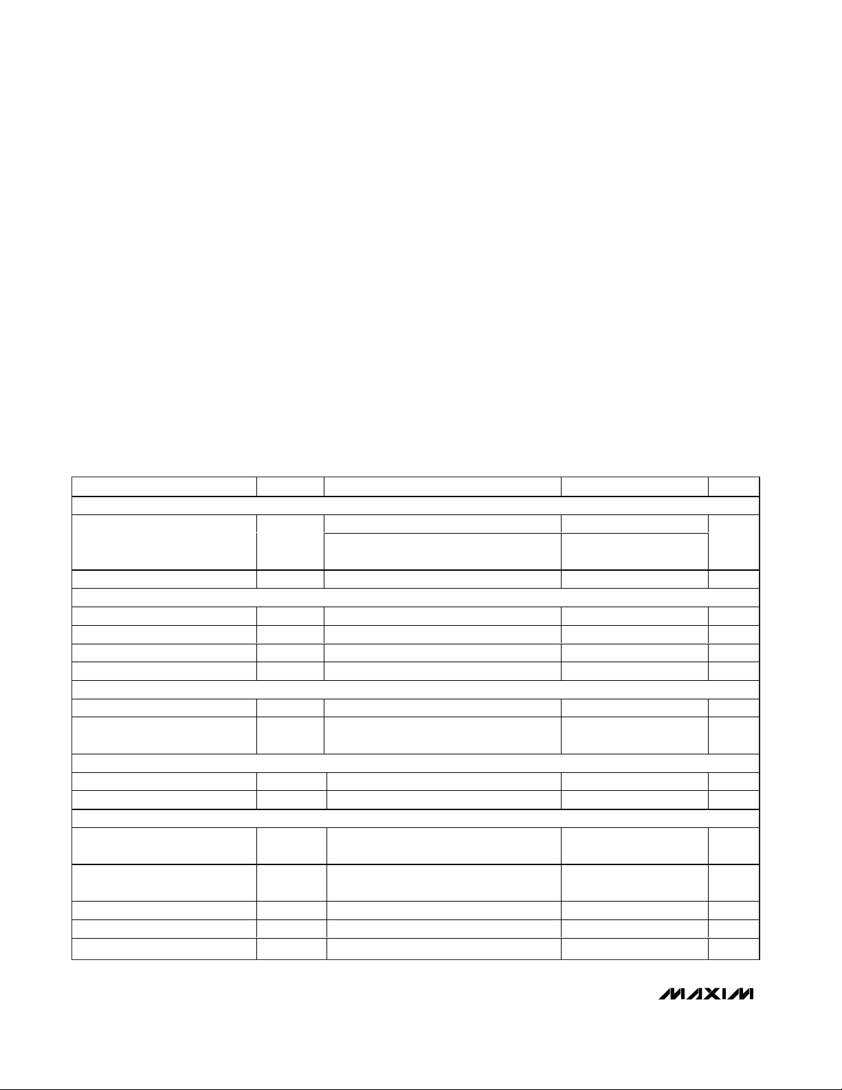
ELECTRICAL CHARACTERISTICS
(VIN= V
REG
= VDD= VEN= +5V, TA= TJ= T
MIN
to T
MAX
, unless otherwise noted, circuit of Figure 6. Typical values are at TA= +25°C.)
(Note 1)
PARAMETER
CONDITIONS
UNITS
SYSTEM SPECIFICATIONS
528
Input Voltage Range V
IN
IN and REG shorted together for +5V
operation
5.5
V
Quiescent Supply Current I
IN
f
OSC
= 500kHz, DH_, DL_ = open 4 20 mA
STARTUP/INTERNAL REGULATOR OUTPUT (REG)
REG Undervoltage Lockout UVLO V
REG
rising 4.0
4.5 V
Hysteresis V
HYST
mV
REG Output Accuracy VIN = 5.8V to 28V, I
SOURCE
= 0 to 65mA
V
REG Dropout VIN < 5.8V, I
SOURCE
= 60mA 0.5 V
INTERNAL REFERENCE
Internal Reference Voltage V
EAN_
EAN_ connected to EAOUT_ (Note 2)
V
Internal Reference Voltage
Accuracy
V
EAN_
VIN = V
REG
= 4.75V to 5.5V or VIN = 5V to
28V, EAN_ connected to EAOUT_ (Note 2)
%
EXTERNAL REFERENCE VOLTAGE OUTPUT (REF)
Accuracy V
REF
I
REF
= 100µA
3.3
V
Load Regulation I
REF
= 0 to 200µA 3.2 3.4 V
MOSFET DRIVERS
p-Channel Output Driver
Impedance
R
ON_P
4 Ω
n-Channel Output Driver
Impedance
R
ON_N
Ω
Output Driver Source Current
2.5 A
Output Driver Sink Current
8A
Nonoverlap Time (Dead Time) t
NO
C
DH_
or C
DL_
= 5nF 30 ns
SYMBOL
MIN TYP MAX
I
, I
DH_
I
, I
DH_
DL_
DL_
4.75
4.15
200
4.75 5.10 5.30
0.6135
-0.9 +0.9
3.23
1.35
0.45 1.35
3.37
Page 3
MAX5066
Configurable, Single-/Dual-Output, Synchronous
Buck Controller for High-Current Applications
_______________________________________________________________________________________ 3
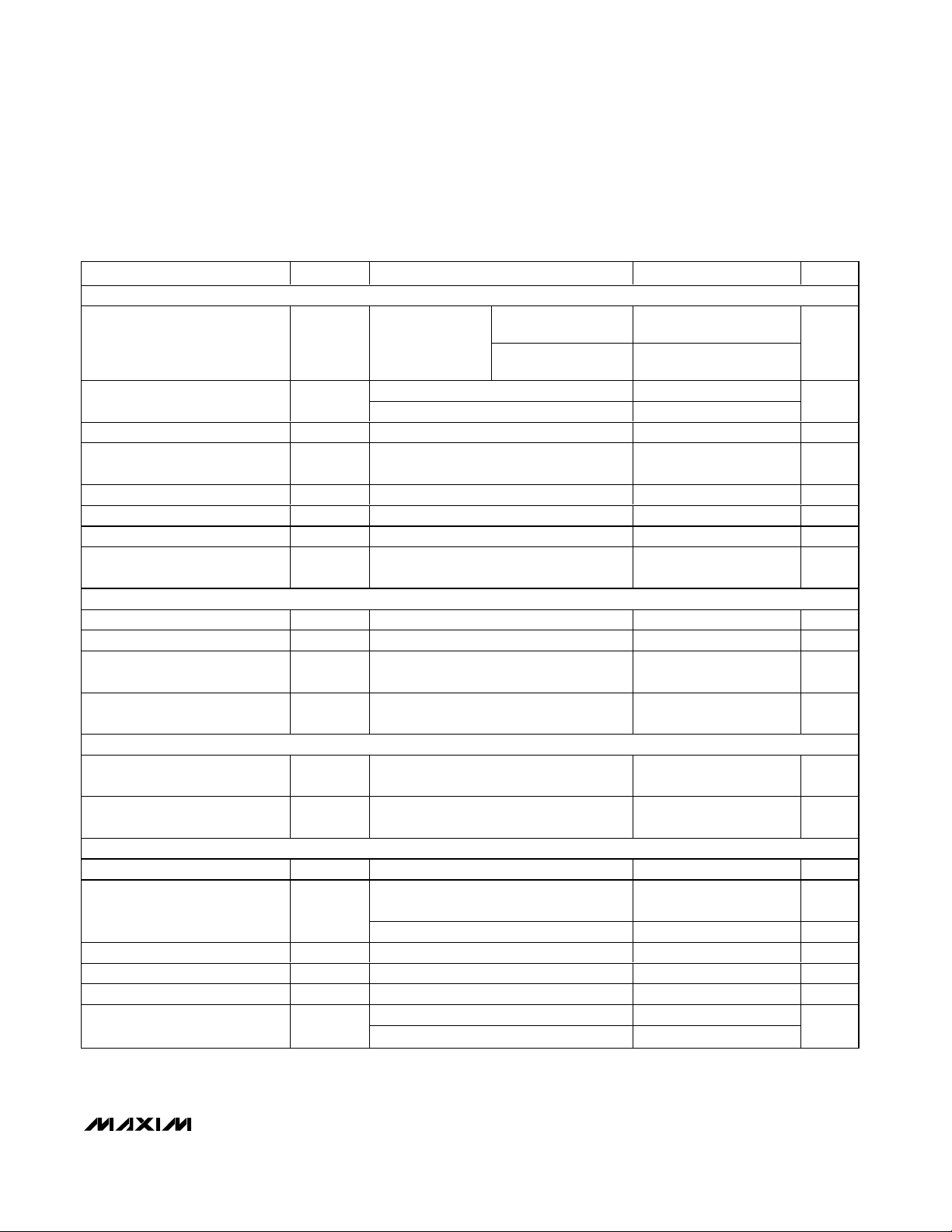
ELECTRICAL CHARACTERISTICS (continued)
(VIN= V
REG
= VDD= VEN= +5V, TA= TJ= T
MIN
to T
MAX
, unless otherwise noted, circuit of Figure 6. Typical values are at TA= +25°C.)
(Note 1)
PARAMETER
CONDITIONS
TYP
UNITS
OSCILLATOR
RRT = 12.4kΩ
Switching Frequency f
SW
1MHz (max)
switching
frequency per
phase
R
RT
= 127kΩ 100
kHz
fSW = 250kHz nominal, RRT = 50kΩ
Switching Frequency Accuracy
f
SW
= 1MHz nominal, RRT = 12.4kΩ
%
RT/CLKIN Output Voltage
V
RT/CLKIN Current Sourcing
Capability
0.5 mA
RT/CLKIN Logic-High Threshold
2.4 V
RT/CLKIN Logic-Low Threshold
0.8 V
RT/CLKIN High Pulse Width
30 ns
RT/CLKIN Synchronization
Frequency Range
kHz
CURRENT LIMIT
Average Current-Limit Threshold
V
CL_
V
CSP_
- V
CSN_
22.5
mV
Reverse Current-Limit Threshold
V
RCL_
V
CSP_
- V
CSN_
mV
Cycle-by-Cycle Current-Limit
Threshold
V
CLpk_VCSP_
- V
CSN_
52.5 mV
Cycle-by-Cycle Current-Limit
Response Time
t
R
260 ns
DIGITAL FAULT INTEGRATION (DF_)
Number of Switching Cycles to
Shutdown in Current-Limit
NS
DF_
Clock
cycles
Number of Switching Cycles to
Recover from Shutdown
NR
DF_
Clock
cycles
CURRENT-SENSE AMPLIFIER
CSP_ to CSN_ Input Resistance R
CS_
kΩ
VIN = V
REG
= 4.75V to 5.5V or
V
IN
= 5V to 10V
V
Common-Mode Range
)
VIN = 7V to 28V
V
Input Offset Voltage
)
100 µV
Amplifier Gain A
V(CS)
36 V/V
-3dB Bandwidth f
-3dB
4
MHz
V
CSP_
= 5.5V, sinking 120
CSP_ Input Bias Current I
CSA(IN)
V
CSP_
= 0V, sourcing 30
µA
SYMBOL
V
V
RT/CLKIN_H
V
RT/CLKIN_L
V
RT/CLKIN
I
RT/CLKIN
t
RT/CLKIN
f
RT/CLKIN
CMR(CS
V
OS(CS
MIN
MAX
1000
-7.5 +7.5
-10 +10
1.225
200 2000
20.4
24.75
-3.13 -1.63 -0.1
32,768
524,288
1.9835
-0.3 +3.6
-0.3 +5.5
Page 4
MAX5066
Configurable, Single-/Dual-Output, Synchronous
Buck Controller for High-Current Applications
4 _______________________________________________________________________________________
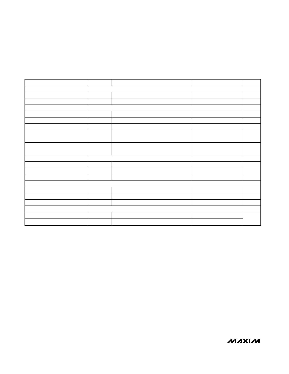
ELECTRICAL CHARACTERISTICS (continued)
(VIN= V
REG
= VDD= VEN= +5V, TA= TJ= T
MIN
to T
MAX
, unless otherwise noted, circuit of Figure 6. Typical values are at TA= +25°C.)
(Note 1)
PARAMETER
SYMBOL
CONDITIONS
MIN
TYP
MAX
UNITS
CURRENT-ERROR AMPLIFIER (CEA_)
Transconductance g
M
550 µS
Open-Loop Gain
)
No load 50 dB
VOLTAGE ERROR AMPLIFIER (EAOUT_)
Open-Loop Gain
)
70 dB
Unity-Gain Bandwidth f
UGEA
3
MHz
EAN_ Input Bias Current
)
V
EAN_
= 2.0V 100 nA
Error Amplifier Output Clamping
High Voltage
V
CLMP_HI
(EA)
With respect to V
CM
1.14 V
Error Amplifier Output Clamping
Low Voltage
V
CLMP_LO
(EA)
With respect to V
CM
V
EN INPUT
EN Input High Voltage V
ENH
EN rising
EN Hysteresis 0.05
V
EN Input Leakage Current I
EN
-1 +1 µA
MODE INPUT
MODE Logic-High Threshold
2.4 V
MODE Logic-Low Threshold
0.8 V
MODE Input Pulldown
5µA
THERMAL SHUTDOWN
Thermal Shutdown T
SHDN
160
Thermal Shutdown Hysteresis T
HYST
10
°C
Note 1: The device is 100% production tested at TA= +85°C (MAX5066EUI). Limits at -40°C and +25°C and TA= TJ= +125°C
(MAX5066AUI) are guaranteed by design.
Note 2: The internal reference voltage accuracy is measured at the negative input of the error amplifiers (EAN_). Output voltage
accuracy must include external resistor-divider tolerances.
A
VOL(CEA
A
VOL(EA
I
BIAS(EA
V
MODE_H
V
MODE_L
I
PULLDWN
-0.234
1.204 1.222 1.240
Page 5
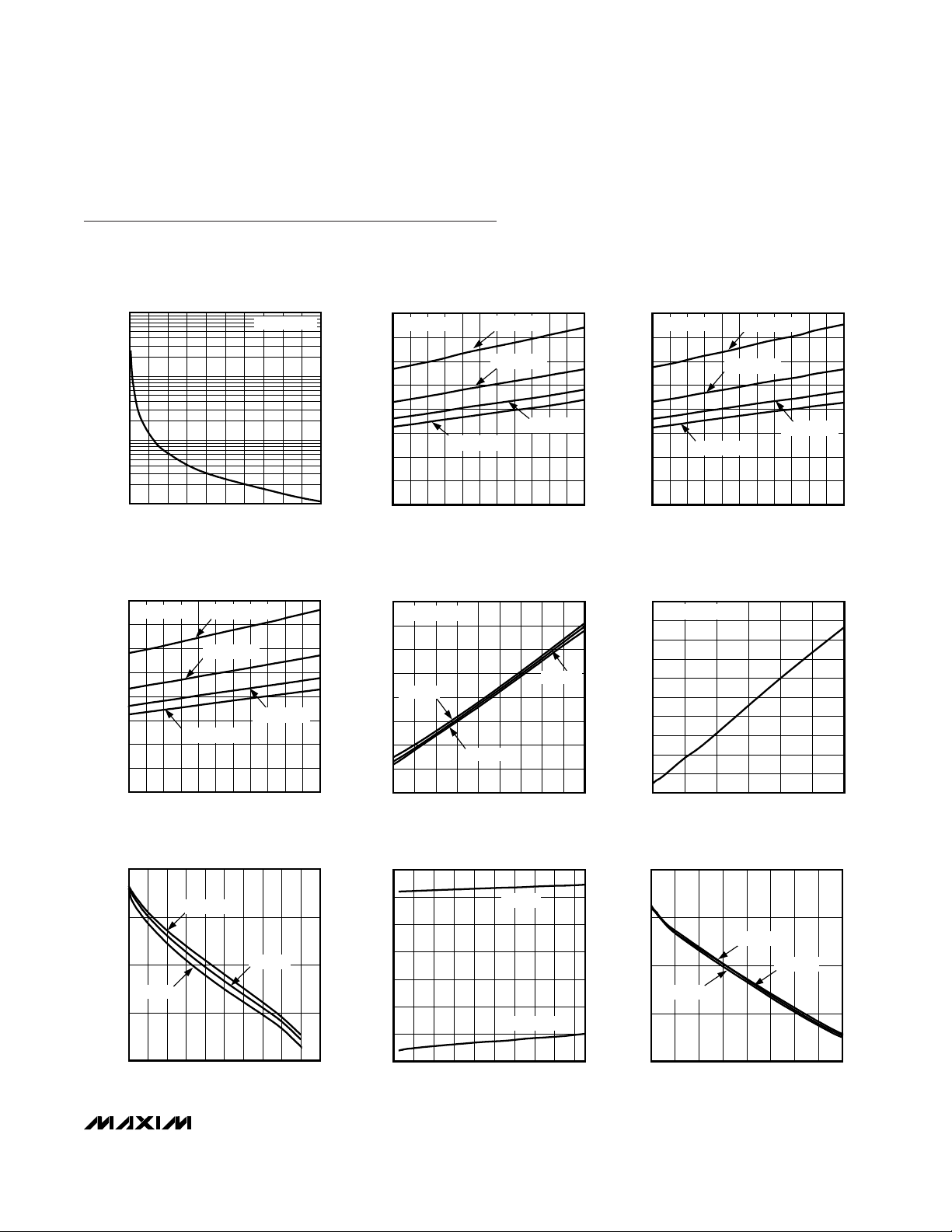
OSCILLATOR FREQUENCY vs. R
T
MAX5066 toc01
RT (kΩ)
OSCILLATOR FREQUENCY (kHz)
900800700600500400300200100
100
1000
10,000
10
01000
CDH = CDL = 0
SUPPLY CURRENT
vs. TEMPERATURE AND FREQUENCY
(V
IN
= 5V)
MAX5066 toc02a
TEMPERATURE (°C)
SUPPLY CURRENT (mA)
11095-25 -10 5 35 50 6520 80
2
4
6
8
10
12
14
16
0
-40 125
CDH = CDL = 0
fSW = 1MHz
fSW = 250kHz
fSW = 500kHz
fSW = 125kHz
SUPPLY CURRENT
vs. TEMPERATURE AND FREQUENCY
(V
IN
= 12V)
MAX5066 toc02b
TEMPERATURE (°C)
SUPPLY CURRENT (mA)
11095-25 -10 5 35 50 6520 80
2
4
6
8
10
12
14
16
0
-40 125
CDH = CDL = 0
fSW = 1MHz
fSW = 250kHz
fSW = 500kHz
fSW = 125kHz
SUPPLY CURRENT
vs. TEMPERATURE AND FREQUENCY
(V
IN
= 24V)
MAX5066 toc02c
TEMPERATURE (°C)
SUPPLY CURRENT (mA)
11095-25 -10 5 35 50 6520 80
2
4
6
8
10
12
14
16
0
-40 125
CDH = CDL = 0
fSW = 1MHz
fSW = 250kHz
fSW = 500kHz
fSW = 125kHz
SUPPLY CURRENT
vs. OSCILLATOR FREQUENCY
MAX5066 toc03
FREQUENCY (kHz)
SUPPLY CURRENT (mA)
18001600400 600 800 12001000 1400
7
8
9
10
11
12
13
14
6
200 2000
C
DH_
= C
DL_
= 0
VIN = 24V
VIN = 5V
VIN = 12V
SUPPLY CURRENT
vs. DRIVER LOAD CAPACITANCE
MAX5066 toc04
C
LOAD
(nF)
SUPPLY CURRENT (mA)
252015105
10
20
30
40
50
60
70
80
90
100
0
030
C
LOAD
= CDH = C
DL
REG LOAD REGULATION
MAX5066 toc05
I
REG
(mA)
V
REG
(V)
908070605040302010
4.95
5.00
5.05
5.10
4.90
0100
VIN = 12V
VIN = 24V
VIN = 5.5V
REG LINE REGULATION
MAX5066 toc06
VIN (V)
V
REG
(V)
2321191715131197
4.98
5.00
5.02
5.04
5.06
5.08
5.10
4.96
5
I
REG
= 0
I
REG
= 60mA
REF LOAD REGULATION
MAX5066 toc07
I
REF
(µA)
V
REF
(V)
700600500400300200100
3.290
3.295
3.300
3.305
3.285
0800
VIN = 24V
VIN = 5V
VIN = 12V
Typical Operating Characteristics
(Circuit of Figure 6, TA= +25°C, unless otherwise noted. VIN= 12V, V
OUT1
= 0.8V, V
OUT2
= 1.3V, fSW= 500kHz per phase.)
MAX5066
Configurable, Single-/Dual-Output, Synchronous
Buck Controller for High-Current Applications
_______________________________________________________________________________________ 5
Page 6
MAX5066
Configurable, Single-/Dual-Output, Synchronous
Buck Controller for High-Current Applications
6 _______________________________________________________________________________________
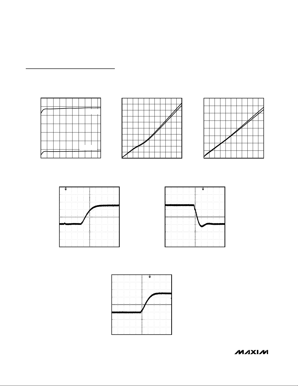
REF LINE REGULATION
MAX5066 toc08
VIN (V)
V
REF
(V)
232119171513119
7
3.297
3.298
3.299
3.300
3.301
3.302
3.303
3.296
5
I
REF
= 200µA
I
REF
= 0
DRIVER RISE TIME
vs. LOAD CAPACITANCE
MAX5066 toc09
C
LOAD
(nF)
t
RISE
(ns)
201814 164 6 8 10 122
10
20
30
40
50
60
70
80
90
100
0
022
DH
DL
DRIVER FALL TIME
vs. LOAD CAPACITANCE
MAX5066 toc10
C
LOAD
(nF)
t
FALL
(ns)
201814 164 6 8 10 122
5
10
15
20
25
30
35
40
0
022
DH
DL
HIGH-SIDE DRIVER RISE TIME
(V
IN
= 12V, C
LOAD
= 10nF)
MAX5066 toc11
DH_
2V/div
20ns/div
HIGH-SIDE DRIVER FALL TIME
(V
IN
= 12V, C
LOAD
= 10nF)
MAX5066 toc12
DH_
2V/div
20ns/div
LOW-SIDE DRIVER RISE TIME
(V
IN
= 12V, C
LOAD
= 10nF)
MAX5066 toc13
DL_
2V/div
20ns/div
Typical Operating Characteristics (continued)
(Circuit of Figure 6, TA= +25°C, unless otherwise noted. VIN= 12V, V
OUT1
= 0.8V, V
OUT2
= 1.3V, fSW= 500kHz per phase.)
Page 7
MAX5066
Configurable, Single-/Dual-Output, Synchronous
Buck Controller for High-Current Applications
_______________________________________________________________________________________ 7
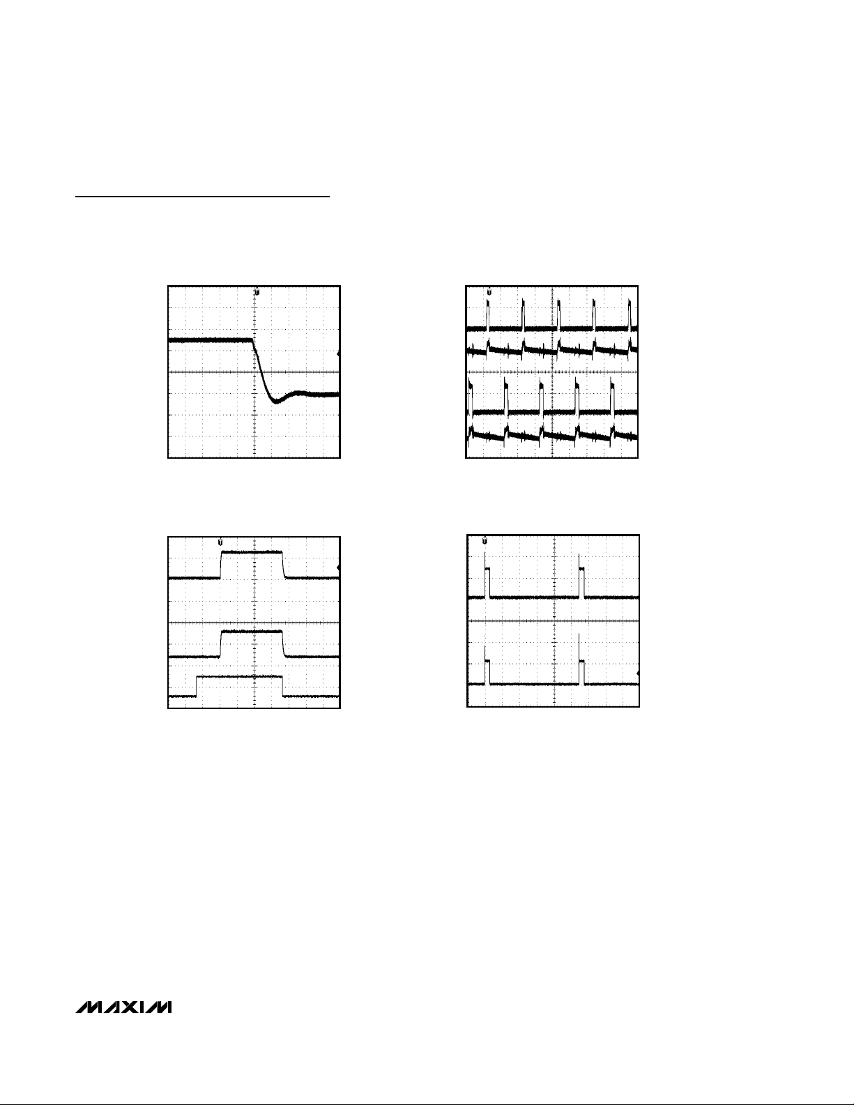
LOW-SIDE DRIVER FALL TIME
(V
IN
= 12V, C
LOAD
= 10nF)
MAX5066 toc14
DL_
2V/div
20ns/div
OUT1/OUT2 OUT-OF-PHASE WAVEFORMS
(V
OUT1
= 0.8V, V
OUT2
= 1.3V)
MAX5066 toc15
OUT1
100mV/div
10µs/div
OUT2
100mV/div
LX2
10V/div
LX1
10V/div
TURN-ON/-OFF WAVEFORMS
(I
OUT1
= I
OUT2
= 10A)
MAX5066 toc16
2ms/div
EN
5V/div
V
OUT2
1V/div
V
OUT1
1V/div
SHORT-CIRCUIT CURRENT WAVEFORMS
(V
IN
= 5V)
MAX5066 toc17
200ms/div
I
OUT2
10A/div
I
OUT1
10A/div
Typical Operating Characteristics (continued)
(Circuit of Figure 6, TA= +25°C, unless otherwise noted. VIN= 12V, V
OUT1
= 0.8V, V
OUT2
= 1.3V, fSW= 500kHz per phase.)
Page 8

MAX5066
Configurable, Single-/Dual-Output, Synchronous
Buck Controller for High-Current Applications
8 _______________________________________________________________________________________
Pin Description
PIN NAME FUNCTION
1 CSN2
Current-Sense Differential Amplifier Negative Input for Output2. Connect CSN2 to the negative
terminal of the sense resistor. The differential voltage between CSP2 and CSN2 is internally amplified
by the current-sense amplifier (A
V(CS)
= 36V/V).
2 CSP2
Current-Sense Differential Amplifier Positive Input for Output2. Connect CSP2 to the positive terminal
of the sense resistor. The differential voltage between CSP2 and CSN2 is internally amplified by the
current-sense amplifier (A
V(CS)
= 36V/V).
3 EAOUT2
Voltage Error-Amplifier Output2. Connect to an external gain-setting feedback resistor. The erroramplifier gain determines the output voltage load regulation for adaptive voltage positioning. This
output also serves as the compensation network connection from EAOUT2 to EAN2. A resistive
network results in a drooped output voltage regulation characteristic. An integrator configuration
results in very tight output voltage regulation (see the Adaptive Voltage Positioning section).
4 EAN2
Voltage Error-Amplifier Inverting Input for Output2. Connect a resistive divider from V
OUT2
to EAN2 to
AGND to set the output voltage. A compensation network connects from EAOUT2 to EAN2. A
resistive network results in a drooped output-voltage-regulation characteristic. An integrator
configuration results in very tight output-voltage regulation (see the Adaptive Voltage Positioning
section).
5 CLP2
Current-Error Amplifier Output2. Compensate the current loop by connecting an R-C network from
CLP2 to AGND.
6 REF
3.3V Reference Output. Bypass REF to AGND with a minimum 0.1µF ceramic capacitor. REF can
source up to 200µA for external loads.
7 RT/CLKIN
External Clock Input or Internal Frequency-Setting Connection. Connect a resistor from RT/CLKIN to
AGND to set the switching frequency. Connect an external clock at RT/CLKIN for external frequency
synchronization.
8 AGND Analog Ground
9 MODE
Mode Function Input. MODE selects between a single-output dual phase or a dual-output buck
regulator. When MODE is grounded, VEA1 and VEA2 connect to CEA1 and CEA2, respectively (see
Figure 1) and the device operates as a two-output, out-of-phase buck regulator. When MODE is
connected to REG (logic high), VEA2 is disconnected and VEA1 is routed to both CEA1 and CEA2.
10 CLP1
Current-Error Amplifier Output1. Compensate the current loop by connecting an R-C network from
CLP1 to AGND.
11 EAN1
Voltage Error Amplifier Inverting Input for Output1. Connect a resistive divider from V
OUT1
to EAN1 to
regulate the output voltage. A compensation network connects from EAOUT1 to EAN1. A resistive
network results in a drooped output-voltage-regulation characteristic. An integrator configuration
results in very tight output voltage regulation (see the Adaptive Voltage Positioning section).
12 EAOUT1
Voltage Error Amplifier Output1. Connect to an external gain-setting feedback resistor. The error
amplifier gain determines the output-voltage-load regulation for adaptive voltage positioning. This
output also serves as the compensation network connection from EAOUT1 to EAN1. A resistive
network results in a drooped output-voltage-regulation characteristic. An integrator configuration
results in very tight output-voltage regulation (see the Adaptive Voltage Positioning section).
13 CSP1
Current-Sense Differential Amplifier Positive Input for Output1. Connect CSP1 to the positive terminal
of the sense resistor. The differential voltage between CSP1 and CSN1 is internally amplified by the
current-sense amplifier (A
V(CS)
= 36V/V).
Page 9

MAX5066
Configurable, Single-/Dual-Output, Synchronous
Buck Controller for High-Current Applications
_______________________________________________________________________________________ 9
Detailed Description
The MAX5066 switching power-supply controller can
be configured in two ways. With the MODE input high, it
operates as a single-output, dual-phase, step-down
switching regulator where each output is 180° out of
phase. With the MODE pin connected low, the
MAX5066 operates as a dual-output, step-down switching regulator. The average current-mode control topology of the MAX5066 offers high-noise immunity while
having benefits similar to those of peak current-mode
control. Average current-mode control has the intrinsic
ability to accurately limit the average current sourced
by the converter during a fault condition. When a fault
condition occurs, the error amplifier output voltage
(EAOUT1 or EAOUT2) that connects to the positive
input of the transconductance amplifier (CA1 or CA2) is
clamped thus limiting the output current.
The MAX5066 contains all blocks necessary for two
independently regulated average current-mode PWM
regulators. It has two voltage error amplifiers (VEA1
and VEA2), two current-error amplifiers (CEA1 and
CEA2), two current-sensing amplifiers (CA1 and CA2),
two PWM comparators (CPWM1 and CPWM2), and drivers for both low- and high-side power MOSFETs (see
Figure 1). Each PWM section is also equipped with a
pulse-by-pulse, current-limit protection and a fault integration block for hiccup protection.
Pin Description (continued)
PIN NAME FUNCTION
14 CSN1
Current-Sense Differential Amplifier Negative Input for Output1. Connect CSN1 to the negative
terminal of the sense resistor. The differential voltage between CSP1 and CSN1 is internally amplified
by the current-sense amplifier (A
V(CS)
= 36V/V).
15, 28 EN
Output Enable. A logic low shuts down both channel MOSFET drivers. Pins 15 and 28 must be tied
together externally.
16 BST1
Boost Flying Capacitor Connection. Reservoir capacitor connection for the high-side MOSFET driver
supply. Connect a 0.47µF ceramic capacitor between BST1 and LX1.
17 DH1 High-Side Gate Driver Output1. DH1 drives the gate of the high-side MOSFET.
18 LX1
External inductor connection and source connection for the high-side MOSFET for Output1. LX1 also
serves as the return terminal for the high-side MOSFET driver.
19 DL1 Low-Side Gate Driver Output1. Gate driver output for the synchronous MOSFET.
20 V
DD
Supply Voltage for Low-Side Drivers. REG powers VDD. Connect a parallel combination of 0.1µF and
1µF ceramic capacitors from V
DD
to PGND and a 1Ω resistor from VDD to REG to filter out the high-
peak currents of the driver from the internal circuitry.
21 REG
Internal 5V Regulator Output. REG is derived internally from IN and is used to power the internal bias
circuitry. Bypass REG to AGND with a 4.7µF ceramic capacitor.
22 IN Supply Voltage Connection. Connect IN to a 5V to 28V input supply.
23 PGND
Power Ground. Source connection for the low-side MOSFET. Connect V
DD
’s bypass capacitor returns
to PGND.
24 DL2 Low-Side Gate Driver Output2. Gate driver for the synchronous MOSFET.
25 LX2
External inductor connection and source connection for the high-side MOSFET for Output2. Also
serves as the return terminal for the high-side MOSFET driver.
26 DH2 High-Side Gate Driver Output2. DH2 drives the gate of the high-side MOSFET.
27 BST2
Boost Flying Capacitor Connection. Reservoir capacitor connection for the high-side MOSFET driver
supply. Connect a 0.47µF ceramic capacitor between BST2 and LX2.
EP EP Exposed Pad. Connect exposed pad to ground plane.
Page 10

MAX5066
Configurable, Single-/Dual-Output, Synchronous
Buck Controller for High-Current Applications
10 ______________________________________________________________________________________
An oscillator, with an externally programmable frequency generates two clock pulse trains and two ramps for
both PWM sections. The two clocks and the two ramps
are 180° out of phase with each other.
A linear regulator (REG) generates the 5V to supply the
device. This regulator has the output-current capability
necessary to provide for the MAX5066’s internal circuitry and the power for the external MOSFET’s gate drivers. A low-current linear regulator (REF) provides a
precise 3.3V reference output and is capable of driving
loads of up to 200µA. Internal UVLO circuitry ensures
that the MAX5066 starts up only when V
REG
and V
REF
are at the correct voltage levels to guarantee safe operation of the IC and of the power MOSFETs.
Finally, a thermal-shutdown feature protects the device
during thermal faults and shuts down the MAX5066
when the die temperature exceeds +160°C.
16
17
18
19
BST1
DH1
LX1
DL1
20
27
26
25
24
23
BST2
DH2
LX2
DL2
PGND
V
DD
2
CSP2
1
CSN2
13
CSP1
14
CSN1
CA1
11
EAN1
6
REF
AGND
8
EN
15
EN
28
CA2
CPWM1
CPWM2
7
RT/CLKIN
CEA1
CEA2
12EAOUT1
9
MODE
3
EAOUT2
5
CLP2
10
CLP1
22
IN
21
REG
1.225V
1.225V
THERMAL
SHUTDOWN
V
DD
MUX
4
EAN2
CEN
VEA1
DF1 AND
HICCUP
LOGIC
EXTERNAL FREQUENCY SYNC
0°
CONTROL
AND DRIVER
LOGIC 1
CONTROL
AND DRIVER
LOGIC 2
DF2 AND
HICCUP
LOGIC
OSCILLATOR
AND PHASE
SPLITTER
180°
2V
P-P
RAMP
V
REG
= 5V
FOR INTERNAL
BIASING
UVLO
V
REF
= 3.3V
UV33
V
INTREF
= 0.61V
VEA2
CEN
2V
P-P
RAMP
Figure 1. Block Diagram
Page 11

MAX5066
Configurable, Single-/Dual-Output, Synchronous
Buck Controller for High-Current Applications
______________________________________________________________________________________ 11
Dual-Output/Dual-Phase Select (MODE)
The MAX5066 can operate as a dual-output independently regulated buck converter, or as a dual-phase,
single-output buck converter. The MODE input selects
between the two operating modes. When MODE is
grounded (logic low), VEA1 and VEA2 connect to CEA1
and CEA2, respectively (see Figure 1) and the device
operates as a two-output DC-DC converter. When
MODE is connected to REG (logic high), VEA2 is disconnected and VEA1 is routed to both CEA1 and CEA2
and the device works as a dual-phase, single-output
buck regulator with each output 180° out of phase with
respect to each other.
Supply Voltage Connections (VIN/V
REG
)
The MAX5066 accepts a wide input voltage range at IN
of 5V to 28V. An internal linear regulator steps down V
IN
to 5.1V (typ) and provides power to the MAX5066. The
output of this regulator is available at REG. For VIN=
4.75V to 5.5V, connect IN and REG together externally.
REG can supply up to 65mA for external loads. Bypass
REG to AGND with a 4.7µF ceramic capacitor for highfrequency noise rejection and stable operation.
REG supplies the current for both the MAX5066’s internal circuitry and for the MOSFET gate drivers (when
connected externally to VDD), and can source up to
65mA. Calculate the maximum bias current (I
BIAS
) for
the MAX5066:
where IINis the quiescent supply current into IN (4mA,
typ), Q
GQ1
, Q
GQ2
, Q
GQ3
, Q
GQ4
are the total gate
charges of MOSFETs Q1 through Q4 at VGS= 5V (see
Figure 6), and fSWis the switching frequency of each
individual phase.
Low-Side MOSFET Driver Supply (VDD)
VDDis the power input for the low-side MOSFET drivers. Connect the regulator output REG externally to
VDDthrough an R-C lowpass filter. Use a 1Ω resistor
and a parallel combination of 1µF and 0.1µF ceramic
capacitors to filter out the high peak currents of the
MOSFET drivers from the sensitive internal circuitry.
High-Side MOSFET Drive Supply (BST_)
BST1 and BST2 supply the power for the high-side
MOSFET drivers for output 1 and output 2, respectively.
Connect BST1 and BST2 to VDDthrough rectifier
diodes D1 and D2 (see Figure 6). Connect a 0.1µF
ceramic capacitor between BST_ and LX_.
Minimize the trace inductance from BST_ and VDDto
rectifier diodes, D1 and D2, and from BST_ and LX_ to
the boost capacitors, C8 and C9 (see Figure 6). This is
accomplished by using short, wide trace lengths.
Undervoltage Lockout (UVLO)/
Power-On Reset (POR)/Soft-Start
The MAX5066 includes an undervoltage lockout
(UVLO) with hysteresis, and a power-on reset circuit for
converter turn-on and monotonic rise of the output voltage. The UVLO threshold monitors V
REG
and is internally set between 4.0V and 4.5V with 200mV of
hysteresis. Hysteresis eliminates “chattering” during
startup. Most of the internal circuitry, including the
oscillator, turns on when V
REG
reaches 4.5V. The
MAX5066 draws up to 4mA (typ) of current before
V
REG
reaches the UVLO threshold.
The compensation network at the current-error amplifiers (CLP1 and CLP2) provides an inherent soft-start of
the output voltage. It includes (R14 and C10) in parallel
with C11 at CLP1 and (R15 and C12) in parallel with
C13 at CLP2 (see Figure 6). The voltage at the currenterror amplifier output limits the maximum current available to charge the output capacitors. The capacitor at
CLP_ in conjunction with the finite output-drive current
of the current-error amplifier yields a finite rise time for
the output current and thus the output voltage.
Setting the Switching Frequency (fSW)
An internal oscillator generates the 180oout-of-phase
clock signals required for both PWM modulators. The
oscillator also generates the 2V
P-P
voltage ramps necessary for the PWM comparators. The oscillator frequency can be set from 200kHz to 2MHz by an external
resistor (RT) connected from RT/CLKIN to AGND (see
Figure 6). The equation below shows the relationship
between RTand the switching frequency:
where R
RT
is in ohms and f
SW(PER PHASE)
= f
OSC
/2.
Use RT/CLKIN as a clock input to synchronize the
MAX5066 to an external frequency (f
RT/CLKIN
). Applying
an external clock to RT/CLKIN allows each PWM section
to work at a frequency equal to f
RT/CLKIN
/2. An internal
comparator with a 1.6V threshold detects f
RT/CLKIN
. If
f
RT/CLKIN
is present, internal logic switches from the
internal oscillator clock, to the clock present at
RT/CLKIN.
Hiccup Fault Protection
The MAX5066 includes overload fault protection circuitry that prevents damage to the power MOSFETs. The
fault protection consists of two digital fault integration
f
R
Hz
OSC
RT
=
×25 10
10
.
IIfQQQQ
BIAS IN SW GQ GQ GQ GQ
=+× +++ ()
1 234
Page 12

MAX5066
Configurable, Single-/Dual-Output, Synchronous
Buck Controller for High-Current Applications
12 ______________________________________________________________________________________
blocks that enable “hiccuping” under overcurrent conditions. This circuit works as follows: for every clock
cycle the current-limit threshold is exceeded, the fault
integration counter increments by one count. Thus, if
the current-limit condition persists, then the counter
reaches its shutdown threshold in 32,768 counts and
shuts down the external MOSFETs. When the MAX5066
shuts down due to a fault, the counter begins to count
down, (since the current-limit condition has ended),
once every 16 clock cycles. Thus, the device counts
down for 524,288 clock cycles. At this point, switching
resumes. This produces an effective duty cycle of
6.25% power-up and 93.75% power-down under fault
conditions. With a switching frequency set to 250kHz,
power-up and power-down times are approximately
131ms and 2.09s, respectively.
Control Loop
The MAX5066 uses an average current-mode control
topology to regulate the output voltage. The control
loop consists of an inner current loop and an outer voltage loop. The inner current loop controls the output
current, while the outer voltage loop controls the output
voltage. The inner current loop absorbs the inductor
pole, reducing the order of the outer voltage loop to
that of a single-pole system. Figure 2 is the block diagram of OUT1’s control loop.
The current loop consists of a current-sense resistor,
R
SENSE
, a current-sense amplifier (CA1), a currenterror amplifier (CEA1), an oscillator providing the carrier ramp, and a PWM comparator (CPWM1). The
precision current-sense amplifier (CA1) amplifies the
sense voltage across R
SENSE
by a factor of 36. The
inverting input to CEA1 senses the output of CA1. The
output of CEA1 is the difference between the voltageerror amplifier output (EAOUT1) and the gained-up voltage from CA1. The RC compensation network
connected to CLP1 provides external frequency compensation for the respective CEA1 (see the
Compensation section). The start of every clock cycle
enables the high-side driver and initiates a PWM oncycle. Comparator CPWM1 compares the output voltage from CEA1 against a 0 to 2V ramp from the
oscillator. The PWM on-cycle terminates when the ramp
voltage exceeds the error voltage from the current-error
amplifier (CEA1).
DRIVE
V
IN
V
OUT1
C
OUT
V
REF
= 0.61V
R
F
C
CFF
C
CF
I
L
R
CF
CSN1
CSP1
CLP1
2V
P-P
R
SENSE
LOAD
R1
R2
CA 1
CEA1
CPWM1
VEA1
Figure 2. Current and Voltage Loops
Page 13

MAX5066
Configurable, Single-/Dual-Output, Synchronous
Buck Controller for High-Current Applications
______________________________________________________________________________________ 13
The outer voltage control loop consists of the voltageerror amplifier (VEA1). The noninverting input (EAN1) is
externally connected to the midpoint of a resistive voltage-divider from OUT1 to EAN1 to AGND. The voltage
loop gain is set by using an external resistor from the
output of this amplifier (EAOUT1) to its inverting input
(EAN1). The noninverting input of (VEA1) is connected
to the 0.61V internal reference.
Peak-Current Comparator
The peak-current comparator (see Figure 3) monitors
the voltage across the current-sense resistor (R
SENSE
)
and provides a fast cycle-by-cycle current limit with a
threshold of 52.5mV. Note that the average current-limit
threshold of 22.5mV still limits the output current during
short-circuit conditions. To prevent inductor saturation,
select an output inductor with a saturation current
specification greater than the average current limit of
22.5mV/R
SENSE
. Proper inductor selection ensures that
only extreme conditions trip the peak-current comparator, such as a damaged output inductor. The typical
propagation delay of the peak current-limit comparator
is 260ns.
Current-Error Amplifier
The MAX5066 has two dedicated transconductance
current-error amplifiers CEA1 and CEA2 with a typical
gMof 550µS and 320µA output sink and source capability. The current-error amplifier outputs (CLP1 and CLP2)
serve as the inverting input to the PWM comparators.
CLP1 and CLP2 are externally accessible to provide frequency compensation for the inner current loops (see
C
CFF
, CCF, and RCFin Figure 2). Compensate the current-error amplifier such that the inductor current down
slope, which becomes the up slope at the inverting
input of the PWM comparator, is less than the slope of
the internally generated voltage ramp (see the
Compensation section).
PWM Comparator and R-S Flip-Flop
The PWM comparator (CPWM1 or CPWM2) sets the
duty cycle for each cycle by comparing the currenterror amplifier output to a 2V
P-P
ramp. At the start of
each clock cycle an R-S flip-flop resets and the highside drivers (DH1 and DH2) turn on. The comparator
sets the flip-flop as soon as the ramp voltage exceeds
the current-error amplifier output voltage, thus terminating the on cycle.
Voltage Error Amplifier
The voltage-error amplifier (VEA_) sets the gain of the
voltage control loop. Its output clamps to 1.14V and
-0.234V relative to VCM= 0.61V. Set the MAX5066 output voltage by connecting a voltage-divider from the
output to EAN_ to GND (see Figure 4). At no load the
output of the voltage error amplifier is zero.
Use the equation below to calculate the no load voltage:
The voltage at full load is given by:
where ∆V
OUT
is the voltage-positioning window
described in the Adaptive Voltage Positioning section.
Adaptive Voltage Positioning
Powering new-generation ICs requires new techniques
to reduce cost, size, and power dissipation. Voltage
positioning (Figure 5) reduces the total number of output capacitors to meet a given transient response
requirement. Setting the no-load output voltage slightly
higher than the output voltage during nominally loaded
conditions allows a larger downward voltage excursion
when the output current suddenly increases.
Regulating at a lower output voltage under a heavy
load allows a larger upward-voltage excursion when
the output current suddenly decreases. A larger
allowed voltage-step excursion reduces the required
number of output capacitors and/or allows the use of
higher ESR capacitors.
The internal 0.61V reference in the MAX5066 has a tolerance of ±0.9%. If we use 0.1% resistors for R1and R2,
we still have another 4% available for the variation in the
output voltage from nominal. This available voltage
range allows us to reduce the total number of output
capacitors to meet a given transient response requirement. This results in a voltage-positioning window as
shown in Figure 5.
From the allowable voltage-positioning window we can
calculate the value of R
F
from the equation below.
where ∆V
OUT
is the allowable voltage-positioning win-
dow, R
SENSE
is the sense resistor, 36 is the current-
sense amplifier gain, and R1is as shown in Figure 4.
MOSFET Gate Drivers (DH_, DL_)
The high-side drivers (DH1 and DH2) and low-side drivers (DL1 and DL2) drive the gates of external n-channel
MOSFETs. The high-peak sink and source current capa-
R
IR R
V
F
OUT SENSE
OUT
=
×××36
1
∆
V
R
R
V
OUT FL OUT()
. =×+
−0 6135 1
1
2
∆
V
R
R
OUT NL()
. =×+
0 6135 1
1
2
Page 14

MAX5066
Configurable, Single-/Dual-Output, Synchronous
Buck Controller for High-Current Applications
14 ______________________________________________________________________________________
bility of these drivers provides ample drive for the fast
rise and fall times of the switching MOSFETs. Faster rise
and fall times result in reduced switching losses. For lowoutput, voltage-regulating applications where the duty
cycle is less than 50%, choose high-side MOSFETs (Q2
and Q4, Figure 6) with a moderate R
DS(ON)
and a very
low gate charge. Choose low-side MOSFETs (Q1 and
Q3, Figure 6) with very low R
DS(ON)
and moderate gate
charge. The driver block also includes a logic circuit that
provides an adaptive nonoverlap time (30ns typical) to
prevent shoot-through currents during transition. Figure 7
shows the dual-phase, single-output buck regulator.
2 x fSW (V/S)
RAMP
CLK
CSP_
CSN_
GM
IN
EN_
1.225V
CLP_
V
DD
BST_
DH_
LX_
DL_
PGND
A
V
= 36
PWM
COMPARATOR
PEAK-CURRENT
COMPARATOR
52.5mV
S
R
Q
Q
gM = 500µS
Figure 3. Current Comparator and MOSFET Driver Logic
LOAD
C
OUT
V
OUT
V
REF
= 0.61V
R
F
R
1
R
2
EAN_
EAOUT_
Figure 4. Voltage Error Amplifier
LOAD (A)
V
CNTR
NO LOAD
1/2 LOAD
FULL LOAD
VOLTAGE-POSITIONING WINDOW
V
CNTR
+ ∆V
OUT
/2
V
CNTR
- ∆V
OUT
/2
Figure 5. Defining the Voltage-Positioning Window
Page 15

MAX5066
Configurable, Single-/Dual-Output, Synchronous
Buck Controller for High-Current Applications
______________________________________________________________________________________ 15
R
T
24.9kΩ
C1
0.22µF
R8
29.4kΩ
V
REG
OR V
REF
R5
4.64kΩ
R4
1.74kΩ
C6
680µF
0.8V/10A
R1
2mΩ
L1
0.5µH
D3
(1A, 30V)
Q1
IRF7832
Q2
IRF7821
C8
0.1µF
D1
(100mA, 30V)
C2
1µF
Q4
IRF7821
D2
(100mA, 30V)
C3
0.1µF
C4
4.7µF
R3
1Ω
C5
10µF
V
IN
1.3V/10A
C9
0.1µF
Q3
IRF7832
D4
(1A, 30V)
L2
0.8µH
R2
2mΩ
R14
1kΩ
C10
15nF
C11
120pF
R15
1kΩ
C12
15nF
C13
120pF
AGND
REF
RT/CLKIN
EN
EN
EAOUT1
EAN1
CSP1
CSN1
DL1
LX1
DH1
BST1
V
DD
IN
REG
BST2
DH2
LX2
DL2
PGND
CSP2
CSN2
EAN2
EAOUT2
MODE
CLP1
CLP2
MAX5066
C7
680µF
R9
60.4kΩ
R7
4.75kΩ
R6
5.11kΩ
EXTERNAL FREQUENCY SYNC
22Ω
22Ω
Figure 6. Dual-Output Buck Regulator
Page 16

MAX5066
Configurable, Single-/Dual-Output, Synchronous
Buck Controller for High-Current Applications
16 ______________________________________________________________________________________
R
T
24.9kΩ
C1
0.22µF
R8
60.4kΩ
V
REG
OR V
REF
R5
4.75kΩ
R4
5.11kΩ
C6
680µF
1.3V/20A
R1
2mΩ
L1
0.8µH
D3
(1A, 30V)
Q1
IRF7832
Q2
IRF7821
C8
0.1µF
D1
(100mA, 30V)
C2
1µF
Q4
IRF7821
D2
(100mA, 30V)
C3
0.1µF
C4
4.7µF
R3
1Ω
C5
10µF
V
IN
C9
0.1µF
Q3
IRF7832
D4
(1A, 30V)
L2
0.8µH
R2
2mΩ
R14
1kΩ
C10
15nF
C11
120pF
R15
1kΩ
C12
15nF
C13
120pF
AGND
REF
RT/CLKIN
EN
EN
EAOUT1
EAN1
CSP1
CSN1
DL1
LX1
DH1
BST1
V
DD
IN
REG
BST2
DH2
LX2
DL2
PGND
CSP2
CSN2
EAN2
EAOUT2
MODE
CLP1
CLP2
MAX5066
EXTERNAL FREQUENCY SYNC
22Ω
22Ω
TO REG
Figure 7. Dual-Phase, Single-Output Buck Regulator
Page 17

MAX5066
Configurable, Single-/Dual-Output, Synchronous
Buck Controller for High-Current Applications
______________________________________________________________________________________ 17
Design Procedures
Inductor Selection
The switching frequency per phase, peak-to-peak ripple
current in each phase, and allowable voltage ripple at
the output, determine the inductance value. Selecting
higher switching frequencies reduces the inductance
requirement, but at the cost of lower efficiency due to
the charge/discharge cycle of the gate and drain
capacitances in the switching MOSFETs. The situation
worsens at higher input voltages, since capacitive
switching losses are proportional to the square of the
input voltage. Lower switching frequencies on the other
hand will increase the peak-to-peak inductor ripple current (∆I
L
) and therefore increase the MOSFET conduction losses (see the Power MOSFET Selection section for
a detailed description of MOSFET power loss).
When using higher inductor ripple current, the ripple
cancellation in the multiphase topology, reduces the
input and output capacitor RMS ripple current. Use the
following equation to determine the minimum inductance value:
Choose ∆ILto be equal to about 30% of the output current per channel. Since ∆ILaffects the output-ripple voltage, the inductance value may need minor adjustment
after choosing the output capacitors for full-rated efficiency. Choose inductors from the standard high-current, surface-mount inductor series available from various
manufacturers. Particular applications may require custom-made inductors. Use high-frequency core material
for custom inductors. High ∆ILcauses large peak-to-peak
flux excursion increasing the core losses at higher
frequencies. The high-frequency operation coupled with
high ∆IL, reduces the required minimum inductance and
even makes the use of planar inductors possible. The
advantages of using planar magnetics include low-profile
design, excellent current sharing between phases due to
the tight control of parasitics, and low cost. For example,
the minimum inductance at VIN= 12V, V
OUT
= 0.8V, ∆I
L
= 3A, and fSW= 500kHz is 0.5µH.
The average current-mode control feature of the
MAX5066 limits the maximum inductor current, which
prevents the inductor from saturating. Choose an
inductor with a saturating current greater than the
worst-case peak inductor current:
where 24.75mV is the maximum average current-limit
threshold for the current-sense amplifier and R
SENSE
is
the sense resistor.
Power MOSFET Selection
When choosing the MOSFETs, consider the total gate
charge, R
DS(ON)
, power dissipation, the maximum
drain-to-source voltage, and package thermal impedance. The product of the MOSFET gate charge and onresistance is a figure of merit, with a lower number
signifying better performance. Choose MOSFETs optimized for high-frequency switching applications. The
average gate-drive current from the MAX5066’s output
is proportional to the total capacitance it drives at DH1,
DH2, DL1, and DL2. The power dissipated in the
MAX5066 is proportional to the input voltage and the
average drive current. See the Supply Voltage
Connection (VIN/V
REG
) and the Low-Side MOSFET
Drives Supply (VDD) sections to determine the maxi-
mum total gate charge allowed from all driver outputs
together.
The losses may be broken into four categories: conduction loss, gate drive loss, switching loss and output loss.
The following simplified power loss equation is true for
both MOSFETs in the synchronous buck-converter:
For the low-side MOSFET, the P
SWITCH
term becomes
virtually zero because the body diode of the MOSFET is
conducting before the MOSFET is turned on.
Tables 1 and 2 describe the different losses and shows
an approximation of the losses during that period.
Input Capacitance
The discontinuous input-current waveform of the buck
converter causes large ripple currents in the input
capacitor. The switching frequency, peak inductor current, and the allowable peak-to-peak voltage ripple
reflected back to the source, dictate the capacitance
requirement. Increasing the number of phases increases the effective switching frequency and lowers the
peak-to-average current ratio, yielding lower input
capacitance requirement. It can be shown that the
worst-case RMS current occurs when only one controller section is operating. The controller section with
PP P P P
LOSS CONDUCTION GATEDRIVE SWITCH OUTPUT
=+++
I
R
I
L PEAK
SENSE
L
_
. =×
+
−
24 75 10
2
3
∆
L
VV V
Vf I
OUT IN MAX OUT
IN SW L
=
−
××
()
()
∆
Page 18

MAX5066
Configurable, Single-/Dual-Output, Synchronous
Buck Controller for High-Current Applications
18 ______________________________________________________________________________________
the highest output power needs to be used in determining the maximum input RMS ripple current requirement.
Increasing the output current drawn from the other outof-phase controller section results in reducing the input
ripple current. A low-ESR input capacitor that can handle the maximum input RMS ripple current of one channel must be used. The maximum RMS capacitor ripple
current is given by:
where I
MAX
is the full load current of the regulator.
V
OUT
is the output voltage of the same regulator and
CINis C5 in Figure 6. The ESR of the input capacitors
wastes power from the input and heats up the capacitor. Reducing the ESR is important to maintain a high
overall efficiency and in reducing the heating of the
capacitors.
Output Capacitors
The worst-case peak-to-peak inductor ripple current,
the allowable peak-to-peak output ripple voltage, and
the maximum deviation of the output voltage during
step loads determine the capacitance and the ESR
requirements for the output capacitors. The output ripple can be approximated as the inductor current ripple
multiplied by the output capacitor’s ESR (R
ESR_OUT
).
The peak-to-peak inductor current ripple is given by:
During a load step, the allowable deviation of the output voltage during the fast transient load dictates the
output capacitance and ESR. The output capacitors
supply the load step until the controller responds with a
greater duty cycle. The response time (t
RESPONSE
)
depends on the closed-loop bandwidth of the regulator. The resistive drop across the capacitor’s ESR and
capacitor discharge causes a voltage drop during a
∆I
VD
Lf
L
OUT
SW
=
−×()1
II
VVV
V
CIN RMS MAX
OUT IN OUT
IN
()
()
≈
−
LOSS DESCRIPTION SEGMENT LOSS
Conduction Loss
Losses associated with MOSFET on-time and
on-resistance. I
RMS
is a function of load current
and duty cycle.
Gate Drive Loss
Losses associated with charging and
discharging the gate capacitance of the
MOSFET every cycle. Use the MOSFET’s (Q
G
)
specification.
Switching Loss
Losses during the drain voltage and drain
current transitions for every switching cycle.
Losses occur only during the Q
GS2
and Q
GD
time period and not during the initial Q
GS1
period. The initial Q
GS1
period is the rise in the
gate voltage from zero to V
TH.
RDH is the high-side MOSFET driver’s onresistance and R
GATE
is the internal gate
resistance of the high-side MOSFET (Q
GD
and
Q
GS2
are found in the MOSFET data sheet).
Output Loss
Losses associated with Q
OSS
of the MOSFET
occur every cycle when the high-side MOSFET
turns on. The losses are caused by both
MOSFETs but are dissipated in the high-side
MOSFET.
Table 1. High-Side MOSFET Losses
PIR
where I
V
V
I
CONDUCTION RMS DS ON
RMS
OUT
IN
LOAD
=×
≈×
2
()
PVQf
GATEDRIVE DD G SW
=××
PVIf
QQ
I
SWITCH IN LOAD SW
GS GD
GATE
=× × ×
+
2
()
where I
V
RR
GATE
DD
DH GATE
=
×+2 ()
P
QQ
Vf
OUTPUT
OSS HS OSS LS
IN SW
=
+
××
2
() ()
Page 19

MAX5066
Configurable, Single-/Dual-Output, Synchronous
Buck Controller for High-Current Applications
______________________________________________________________________________________ 19
load step. Use a combination of SP polymer and
ceramic capacitors for better transient load and ripple/noise performance.
Keep the maximum output-voltage deviation less than
or equal to the adaptive voltage-positioning window
(∆V
OUT
). During a load step, assume a 50% contribu-
tion each from the output capacitance discharge and
the voltage drop across the ESR (∆V
OUT
= ∆V
ESR_
OUT
+ ∆V
Q_OUT
). Use the following equations to calculate
the required ESR and capacitance value:
where I
LOAD_STEP
is the step in load current and
t
RESPONSE
is the response time of the controller.
Controller response time depends on the control-loop
bandwidth. C
OUT
is C6 and C7 in Figure 6.
Current Limit
The average current-mode control technique of the
MAX5066 accurately limits the maximum average output current per phase. The MAX5066 senses the voltage across the sense resistor and limits the maximum
inductor current accordingly. Use the equations below
to calculate the current-sense resistor values:
Due to tolerances involved, the minimum average voltage at which the voltage across the current-sense
resistor is clamped is 20.4mV. Therefore, the minimum
average current limit is set at:
For example, the current-sense resistor:
for a maximum output current of 10A. The standard
value is 2mΩ. Also, adjust the value of the currentsense resistor to compensate for parasitics associated
with the PC board. Select a noninductive resistor with
appropriate wattage rating.
The second type of current limit is the peak current limit
as explained in the Peak-Current Comparator section.
The third current-protection circuit is the hiccup fault
protection as explained in the Hiccup Fault Protection
section. The average current during a short at the output is given by:
Reverse Current Limit
The MAX5066 limits the reverse current when the output
capacitor voltage is higher than the preset output voltage. Calculate the maximum reverse current limit based
on V
CLAMP_LO
and the current-sense resistor R
SENSE
.
I
R
AVG SHORT
SENSE
()
.
=
×
−
141 10
3
R
mV
A
m
SENSE
==
20 4
10
204.. Ω
I
R
LIMIT MIN
SENSE
()
. =×
−
20 4 10
3
I
R
LOAD MAX
SENSE
()
.
=
×
−
24 75 10
3
R
V
I
C
It
V
ESR OUT
ESR OUT
LOAD STEP
OUT
LOAD STEP RESPONSE
Q OUT
_
_
_
_
_
=
=
×
∆
∆
LOSS DESCRIPTION SEGMENT LOSSES
Conduction Loss
Losses associated with MOSFET on-time, I
RMS
is a function of load current and duty cycle.
Gate Drive Loss
Losses associated with charging and
discharging the gate of the MOSFET every
cycle. There is no QGD charging involved in this
MOSFET due to the zero-voltage turn-on. The
charge involved is (Q
G
- QGD).
Table 2. Low-Side MOSFET Losses
PIR
where I
VV
V
I
CONDUCTION RMS DS ON
RMS
IN OUT
IN
LOAD
=×
≈
−
×
2
()
PVQQf
GATEDRIVE DD G GD SW
=×− ×()
Note: The gate drive losses are distributed between the drivers and the MOSFETs in the ratio of the gate driver’s resistance and the
MOSFET’s internal gate resistance.
Page 20

MAX5066
Configurable, Single-/Dual-Output, Synchronous
Buck Controller for High-Current Applications
20 ______________________________________________________________________________________
Output-Voltage Setting
The output voltage is set by the combination of resistors
R1, R2, and RFas described in the Voltage Error Amplifier
section. First select a value for resistor R2. Then calculate
the value of R1 from the following equation:
where V
OUT(NL)
is the voltage at no load. Then find the
value of RFfrom the following equation:
where ∆V
OUT
is the allowable drop in voltage from no
load to full load. R
F
is R8 and R9, R1 is R4 and R6, R2
is R5 and R7 in Figure 6.
Compensation
The MAX5066 uses an average current-mode control
scheme to regulate the output voltage (see Figure 2).
The main control loop consists of an inner current loop
and an outer voltage loop. The voltage error amplifier
(VEA1 and VEA2) provides the controlling voltage for
the current loop in each phase. The output inductor is
“hidden” inside the inner current loop. This simplifies
the design of the outer voltage control loop and also
improves the power-supply dynamics. The objective of
the inner current loop is to control the average inductor
current. The gain-bandwidth characteristic of the current loop can be tailored for optimum performance by
the compensation network at the output of the currenterror amplifier (CEA1 or CEA2). Compared with peak
current-mode control, the current-loop gain crossover
frequency, fC, can be made approximately the same,
but the gain at low frequencies is much higher. This
results in the following advantages over peak currentmode control.
1) The average current tracks the programmed current with a high degree of accuracy.
2) Slope compensation is not required, but there is a
limit to the loop gain at the switching frequency in
order to achieve stability.
3) Noise immunity is excellent.
4) The average current-mode method can be used to
sense and control the current in any circuit branch.
For stability of the current loop, the amplified inductorcurrent downslope at the negative input of the PWM
comparator (CPWM1 and CPWM2) must not exceed
the ramp slope at the comparator’s positive input. This
puts an upper limit on the current-error amplifier gain at
the switching frequency. The inductor current downslope is given by V
OUT
/L where L is the value of the
inductor (L1 and L2 in Figure 6) and V
OUT
is the output
voltage. The amplified inductor current downslope at
the negative input of the PWM comparator is given by:
where R
SENSE
is the current-sense resistor (R1 and R2
in Figure 6) and gMx RCFis the gain of the current-error
amplifier (CEA_) at the switching frequency. The slope
of the ramp at the positive input of the PWM comparator
is 2V x fSW. Use the following equation to calculate the
maximum value of RCF(R14 or R15 in Figure 6).
The highest crossover frequency f
CMAX
is given by:
or alternatively:
Equation (1) can now be rewritten as:
In practical applications, pick the crossover frequency
(fC) in the range of:
First calculate R
CF
in equation 2 above. Calculate C
CF
such that:
where C
CF
is C10 and C12 in Figure 6.
C
fR
CF
CCF
=
×× ×
10
2 π
f
f
f
SW
C
SW
10 2
<< .
R
fL
VR g
CF
C
IN S M
=
××
×××
π
9
2()
f
fV
V
SW
CMAX OUT
IN
=
××2π
f
fV
V
CMAX
SW IN
OUT
=
×
×2π
R
fL
VR g
CF
SW
OUT SENSE M
≤
××
×××
2
36
1()
∆∆VtV
L
RgR
L OUT
SENSE M CF
=× ×××36
R
IR R
V
F
OUT SENSE
OUT
=
×××36
1
∆
R
V
R
OUT NL
1
0 6135
0 6135
2
(.)
.
()
=
−
×
I
R
REVERSE
SENSE
=
×
−
163 10
3
.
Page 21

MAX5066
Configurable, Single-/Dual-Output, Synchronous
Buck Controller for High-Current Applications
______________________________________________________________________________________ 21
Calculate C
CFF
such that:
where C
CFF
is C11 and C13 in Figure 6.
Applications Information
PC Board Layout Guidelines
Careful PC board layout is critical to achieve low losses, low output noise, and clean and stable operation.
This is especially true for dual-phase converters where
one channel can affect the other. Use the following
guidelines for PC board layout:
1) Place the VDD, REG, and the BST1 and BST2
bypass capacitors close to the MAX5066.
2) Minimize all high-current switching loops.
3) Keep the power traces and load connections short.
This practice is essential for high efficiency. Use
thick copper PC boards (2oz or higher) to enhance
efficiency and minimize trace inductance and
resistance.
4) Run the current-sense lines CSP_ and CSN_ very
close to each other to minimize loop areas. Do not
cross these critical signal lines through power circuitry. Sense the current right at the pads of the
current-sense resistors.
5) Place the bank of output capacitors close to the
load.
6) Isolate the power components on the top side from
the analog components on the bottom side with a
ground plane in between.
7) Provide enough copper area around the switching
MOSFETs, inductors, and sense resistors to aid in
thermal dissipation and reducing resistance.
8) Distribute the power components evenly across the
top side for proper heat dissipation.
9) Keep AGND and PGND isolated and connect them
at one single point close to the IC. Do not connect
them together anywhere else.
10) Place all input bypass capacitors for each input as
close to each other as is practical.
C
fR
CFF
CCF
=
×× × ×
1
210π
28
27
26
25
24
23
22
21
20
19
18
17
16
15
1
2
3
4
5
6
7
8
9
10
11
12
13
14
EN
BST2
DH2
LX2
DL2
PGND
EN
IN
REG
V
DD
DL1
LX1
DH1
BST1
CSN1
CSP1
EAOUT1
EAN1
CLP1
MODE
AGND
RT/CLKIN
REF
CLP2
EAN2
EAOUT2
CSP2
CSN2
TSSOP
TOP VIEW
MAX5066
*EXPOSED PADDLE
*CONNECT EXPOSED PAD TO GROUND PLANE.
Pin Configuration
Chip Information
TRANSISTOR COUNT: 6252
PROCESS: BiCMOS
Page 22

MAX5066
Configurable, Single-/Dual-Output, Synchronous
Buck Controller for High-Current Applications
Maxim cannot assume responsibility for use of any circuitry other than circuitry entirely embodied in a Maxim product. No circuit patent licenses are
implied. Maxim reserves the right to change the circuitry and specifications without notice at any time.
22 ____________________Maxim Integrated Products, 120 San Gabriel Drive, Sunnyvale, CA 94086 408-737-7600
© 2005 Maxim Integrated Products Printed USA is a registered trademark of Maxim Integrated Products, Inc.
Package Information
(The package drawing(s) in this data sheet may not reflect the most current specifications. For the latest package outline information,
go to www.maxim-ic.com/packages
.)
TSSOP4.40mm.EPS
PACKAGE OUTLINE, TSSOP 4.40mm BODY
21-0066
1
1
G
 Loading...