

Page 1
General Description
The MAX5062/MAX5063/MAX5064 high-frequency,
125V half-bridge, n-channel MOSFET drivers drive highand low-side MOSFETs in high-voltage applications.
These drivers are independently controlled and their
35ns typical propagation delay, from input to output, are
matched to within 3ns (typ). The high-voltage operation
with very low and matched propagation delay between
drivers, and high source/sink current capabilities in a
thermally enhanced package make these devices suitable for the high-power, high-frequency telecom power
converters. The 125V maximum input voltage range provides plenty of margin over the 100V input transient
requirement of telecom standards. A reliable on-chip
bootstrap diode connected between VDDand BST eliminates the need for an external discrete diode.
The MAX5062A/C and the MAX5063A/C offer both noninverting drivers (see the Selector Guide). The
MAX5062B/D and the MAX5063B/D offer a noninverting
high-side driver and an inverting low-side driver. The
MAX5064A/B offer two inputs per driver that can be
either inverting or noninverting. The MAX5062A/B/C/D
and the MAX5064A feature CMOS (V
DD
/ 2) logic inputs.
The MAX5063A/B/C/D and the MAX5064B feature TTL
logic inputs. The MAX5064A/B include a break-beforemake adjustment input that sets the dead time between
drivers from 16ns to 95ns. The drivers are available in the
industry-standard 8-pin SO footprint and pin configuration, and a thermally enhanced 8-pin SO and 12-pin
(4mm x 4mm) thin QFN packages. All devices operate
over the -40°C to +125°C automotive temperature range.
Applications
Telecom Half-Bridge Power Supplies
Two-Switch Forward Converters
Full-Bridge Converters
Active-Clamp Forward Converters
Power-Supply Modules
Motor Control
Features
♦ HIP2100/HIP2101 Pin Compatible (MAX5062A/
MAX5063A)
♦ Up to 125V Input Operation
♦ 8V to 12.6V VDDInput Voltage Range
♦ 2A Peak Source and Sink Current Drive Capability
♦ 35ns Typical Propagation Delay
♦ Guaranteed 8ns Propagation Delay Matching
Between Drivers
♦ Programmable Break-Before-Make Timing
(MAX5064)
♦ Up to 1MHz Combined Switching Frequency while
Driving 100nC Gate Charge (MAX5064)
♦ Available in CMOS (V
DD
/ 2) or TTL Logic-Level
Inputs with Hysteresis
♦ Up to 15V Logic Inputs Independent of Input
Voltage
♦ Low 2.5pF Input Capacitance
♦ Instant Turn-Off of Drivers During Fault or PWM
Start-Stop Synchronization (MAX5064)
♦ Low 200µA Supply Current
♦ Versions Available With Combination of
Noninverting and Inverting Drivers (MAX5062B/D
and MAX5063B/D)
♦ Available in 8-Pin SO, Thermally Enhanced SO,
and 12-Pin Thin QFN Packages
MAX5062/MAX5063/MAX5064
125V/2A, High-Speed,
Half-Bridge MOSFET Drivers
________________________________________________________________ Maxim Integrated Products 1
PART TEMP RANGE
PIN-
TOP
MARK
MAX5062AASA
8 SO —
MAX5062BASA
8 SO —
MAX5062CASA
8 SO-EP* —
MAX5062DASA
8 SO-EP* —
Ordering Information
PART HIGH-SIDE DRIVER LOW-SIDE DRIVER LOGIC LEVELS PIN COMPATIBLE
MAX5062AASA Noninverting Noninverting CMOS (V
DD
/ 2) HIP 2100IB
MAX5062BASA Noninverting Inverting CMOS (V
DD
/ 2) —
MAX5062CASA Noninverting Noninverting CMOS (V
DD
/ 2) —
MAX5062DASA Noninverting Inverting CMOS (V
DD
/ 2) —
Selector Guide
19-3502; Rev 2; 4/05
For pricing, delivery, and ordering information, please contact Maxim/Dallas Direct! at
1-888-629-4642, or visit Maxim’s website at www.maxim-ic.com.
Selector Guide continued at end of data sheet.
*EP = Exposed paddle.
Ordering Information continued at end of data sheet.
PACKAGE
-40°C to +125°C
-40°C to +125°C
-40°C to +125°C
-40°C to +125°C
Page 2
MAX5062/MAX5063/MAX5064
125V/2A, High-Speed,
Half-Bridge MOSFET Drivers
2 _______________________________________________________________________________________
ABSOLUTE MAXIMUM RATINGS
ELECTRICAL CHARACTERISTICS
(VDD= V
BST
= +8V to +12.6V, VHS= GND = 0V, BBM = open, TA= -40°C to +125°C, unless otherwise noted. Typical values are at
V
DD
= V
BST
= +12V and TA= +25°C.) (Note 1)
Stresses beyond those listed under “Absolute Maximum Ratings” may cause permanent damage to the device. These are stress ratings only, and functional
operation of the device at these or any other conditions beyond those indicated in the operational sections of the specifications is not implied. Exposure to
absolute maximum rating conditions for extended periods may affect device reliability.
(All voltages referenced to GND, unless otherwise noted.)
V
DD
, IN_H, IN_L, IN_L+, IN_L-, IN_H+, IN_H-........-0.3V to +15V
DL, BBM .....................................................-0.3V to (V
DD
+ 0.3V)
HS............................................................................-5V to +130V
DH to HS.....................................................-0.3V to (V
DD
+ 0.3V)
BST to HS ...............................................................-0.3V to +15V
dV/dt at HS ........................................................................50V/ns
Continuous Power Dissipation (T
A
= +70°C)
8-Pin SO (derate 5.9mW/°C above +70°C)...............470.6mW
8-Pin SO With Exposed Pad (derate 19.2mW/°C
above +70°C)......................................................1538.5mW
12-Pin Thin QFN (derate 24.4mW/°C
above +70°C)......................................................1951.2mW
Maximum Junction Temperature .....................................+150°C
Operating Temperature Range .........................-40°C to +125°C
Storage Temperature Range .............................-65°C to +150°C
Lead Temperature (soldering, 10s) .................................+300°C
PARAMETER
CONDITIONS
UNITS
POWER SUPPLIES
Operating Supply Voltage V
DD
(Note 2) 8.0
V
MAX5062_/
MAX5063_
70
VDD Quiescent Supply Current I
DD
IN_H = IN_L = GND
(no switching)
MAX5064_
µA
VDD Operating Supply Current I
DDO
fSW = 500kHz, VDD = +12V 3 mA
BST Quiescent Supply Current I
BST
IN_H = IN_L = GND (no switching) 15 40 µA
BST Operating Supply Current I
BSTOfSW
= 500kHz, VDD = V
BST
= +12V 3 mA
UVLO (VDD to GND)
VDD rising 6.5 7.3 8.0 V
UVLO (BST to HS)
BST rising 6.0 6.9 7.8 V
UVLO Hysteresis 0.5 V
LOGIC INPUT
MAX5062_/MAX5064A,
CMOS (V
DD
/ 2) version
0.67 x
0.55 x
Input-Logic High V
IH_
MAX5063_/MAX5064B, TTL version 2
V
MAX5062_/MAX5064A,
CMOS (V
DD
/ 2) version
0.4 x
0.33 x
Input-Logic Low V
IL_
MAX5063_/MAX5064B, TTL version 1.4 0.8
V
MAX5062_/MAX5064A,
CMOS (V
DD
/ 2) version
1.6
Logic-Input Hysteresis V
HYS
MAX5063_/MAX5064B, TTL version
V
SYMBOL
MIN TYP MAX
12.6
140
120 260
UVLO
VDD
UVLO
BST
V
DD
V
DD
1.65
V
DD
0.25
V
DD
Page 3
MAX5062/MAX5063/MAX5064
125V/2A, High-Speed,
Half-Bridge MOSFET Drivers
_______________________________________________________________________________________ 3
ELECTRICAL CHARACTERISTICS (continued)
(VDD= V
BST
= +8V to +12.6V, VHS= GND = 0V, BBM = open, TA= -40°C to +125°C, unless otherwise noted. Typical values are at
V
DD
= V
BST
= +12V and TA= +25°C.) (Note 1)
PARAMETER
CONDITIONS
UNITS
V
IN_H+
, V
IN_L+
= 0V
V
IN_H-
, V
IN_L-
, V
IN_H
= V
DD
Logic-Input Current I_IN
-1
+1 µA
IN_H+, IN_L+ IN_H, to GND
IN_L to V
DD
for MAX5062B/D,
MAX5063B/D
IN_H-, IN_L-, IN_H, to V
DD
Input Resistance R
IN
1MΩ
Input Capacitance C
IN
2.5 pF
HIGH-SIDE GATE DRIVER
HS Maximum Voltage
V
BST Maximum Voltage
V
TA = +25°C 2.5 3.3
Driver Output Resistance
(Sourcing)
VDD = 12V, IDH = 100mA
(sourcing)
T
A
= +125°C 3.5 4.6
Ω
TA = +25°C 2.1 2.8
Driver Output Resistance
(Sinking)
VDD = 12V, IDH = 100mA
(sinking)
T
A
= +125°C 3.2 4.2
Ω
DH Reverse Current (Latchup
Protection)
(Note 3)
mA
Power-Off Pulldown Clamp
Voltage
V
Peak Output Current (Sourcing) CL = 10nF, VDH = 0V 2 A
Peak Output Current (Sinking)
CL = 10nF, VDH = 12V 2 A
LOW-SIDE GATE DRIVER
TA = +25°C 2.5 3.3
Driver Output Resistance
(Sourcing)
VDD = 12V, IDL = 100mA
(sourcing)
T
A
= +125°C 3.5 4.6
Ω
TA = +25°C 2.1 2.8
Driver Output Resistance
(Sinking)
VDD = 12V, IDL = 100mA
(sinking)
T
A
= +125°C 3.2 4.2
Ω
Reverse Current at DL (Latchup
Protection)
(Note 3)
mA
Power-Off Pulldown Clamp
Voltage
V
DD
= 0V or floating, IDL = 1mA (sinking)
V
Peak Output Current (Sourcing) I
PK_LP
CL = 10nF, VDL = 0V 2 A
Peak Output Current (Sinking) I
PK_LN
CL = 10nF, VDL = 12V 2 A
INTERNAL BOOTSTRAP DIODE
Forward Voltage Drop V
f
I
BST
= 100mA
V
Turn-On and Turn-Off Time t
R
I
BST
= 100mA 40 ns
SYMBOL
V
= VDD for MAX5062B/D, MAX5063B/D
IN_L
V
= 0V for MAX5062A/C, MAX5063A/C
IN_L
V
HS_MAX
V
BST_MAX
R
ON_HP
IN_L for MAX5062A/C, MAX5063A/C to GND
R
ON_HN
V
BST
I
DH_PEAK
= 0V or floating, IDH = 1mA (sinking) 0.94 1.16
R
ON_LP
R
ON_LN
MIN TYP MAX
125
140
400
0.001
400
0.95 1.16
0.91 1.11
Page 4
MAX5062/MAX5063/MAX5064
125V/2A, High-Speed,
Half-Bridge MOSFET Drivers
4 _______________________________________________________________________________________
Note 1: All devices are 100% tested at TA= +125°C. Limits over temperature are guaranteed by design.
Note 2: Ensure that the V
DD
-to-GND or BST-to-HS voltage does not exceed 13.2V.
Note 3: Guaranteed by design, not production tested.
Note 4: Break-before-make time is calculated by t
BBM
= 8ns x (1 + R
BBM
/ 10kΩ).
ELECTRICAL CHARACTERISTICS (continued)
(VDD= V
BST
= +8V to +12.6V, VHS= GND = 0V, BBM = open, TA= -40°C to +125°C, unless otherwise noted. Typical values are at
V
DD
= V
BST
= +12V and TA= +25°C.) (Note 1)
PARAMETER
CONDITIONS
UNITS
SWITCHING CHARACTERISTICS FOR HIGH- AND LOW-SIDE DRIVERS
CL = 1000pF 7
CL = 5000pF 33Rise Time t
R
CL = 10,000pF 65
ns
CL = 1000pF 7
CL = 5000pF 33
Fall Time t
F
CL = 10,000pF 65
ns
CMOS 30 55
Turn-On Propagation Delay Time
t
D_ON
Figure 1, CL = 1000pF
(Note 3)
TTL 35 63
ns
CMOS 30 55
Turn-Off Propagation Delay Time
t
D_OFF
Figure 1, CL = 1000pF
(Note 3)
TTL 35 63
ns
Delay Matching Between
Inverting Input to Output and
Noninverting Input to Output
CL = 1000pF, BBM open for MAX5064,
Figure 1 (Note 3)
28ns
Delay Matching Between DriverLow and Driver-High
CL = 1000pF, BBM open for MAX5064,
Figure 1 (Note 3)
28ns
R
BBM
= 10kΩ 16
R
BBM
= 47kΩ (Notes 3, 4) 40 56 72
Break-Before-Make Accuracy
(MAX5064 Only)
R
BBM
= 100kΩ 95
ns
Internal Nonoverlap 1ns
SYMBOL
t
MATCH1
t
MATCH2
MIN TYP MAX
Page 5
MAX5062/MAX5063/MAX5064
125V/2A, High-Speed,
Half-Bridge MOSFET Drivers
_______________________________________________________________________________________ 5
UNDERVOLTAGE LOCKOUT
(V
DD
AND V
BST
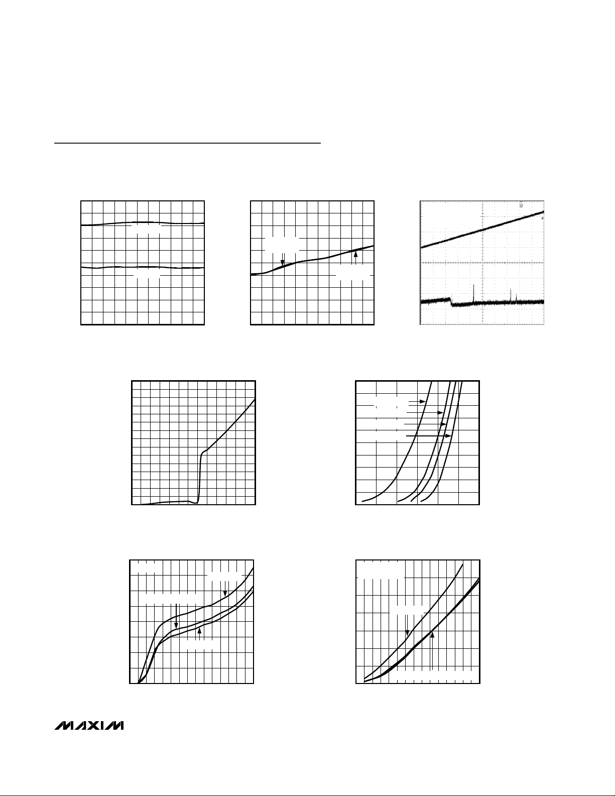
RISING) vs. TEMPERATURE
MAX5062/3/4 toc01
TEMPERATURE (°C)
UVLO (V)
1109565 80-10 5 20 35 50-25
6.6
6.7
6.8
6.9
7.0
7.1
7.2
7.3
7.4
7.5
6.5
-40 125
UVLO
VDD
UVLO
BST
VDD AND BST UNDERVOLTAGE LOCKOUT
HYSTERESIS vs. TEMPERATURE
MAX5062/3/4 toc02
TEMPERATURE (°C)
UVLO HYSTERESIS (V)
1109565 80-10 5 20 35 50-25
0.1
0.2
0.3
0.4
0.5
0.6
0.7
0.8
0.9
1.0
0
-40 125
UVLO
BST
HYSTERESIS
UVLO
VDD
HYSTERESIS
IDD vs. V
DD
MAX5062/3/4 toc03
40µs/div
V
DD
2V/div
500µA/div
0A
0V
I
DD
MAX5064
IN_L-, IN_H- = V
DD
IN_L+, IN_H+ = GND
I
DDO
+ I
BSTO
vs. V
DD
(fSW = 250kHz)
MAX5062/3/4 toc04
VDD (V)
I
DDO
+
I
BSTO
(mA)
1210 11345678912
1.0
0.8
0.6
0.4
0.2
1.2
1.4
1.6
1.8
2.0
2.2
2.4
2.6
2.8
3.0
0
013
0
60
40
20
80
100
120
140
160
180
200
0.5 0.70.6 0.8 0.9 1.0 1.1
INTERNAL BST DIODE
(I-V) CHARACTERISTICS
MAX5062/3/4 toc05
VDD - V
BST
(V)
I
DIODE
(mA)
TA = +125°C
TA = +25°C
TA = 0°C
TA = -40°C
0
60
40
20
80
100
120
140
160
0426810153 7 9 1112131415
VDD QUIESCENT CURRENT
vs. V
DD
(NO SWITCHING)
MAX5062/3/4 toc06
VDD (V)
I
DD
(µA)
TA = -40°C
TA = +125°C
MAX5064
TA = +25°C, TA = 0°C
0
6
3
9
12
15
18
21
0426810153 7 9 1112131415
BST QUIESCENT CURRENT
vs. BST VOLTAGE
MAX5062/3/4 toc07
V
BST
(V)
I
BST
(µA)
V
BST
= VDD + 1V,
NO SWITCHING
TA = +125°C
TA = -40°C, TA = 0°C, TA = +25°C
Typical Operating Characteristics
(Typical values are at VDD= V
BST
= +12V and TA= +25°C, unless otherwise specified.)
Page 6
MAX5062/MAX5063/MAX5064
125V/2A, High-Speed,
Half-Bridge MOSFET Drivers
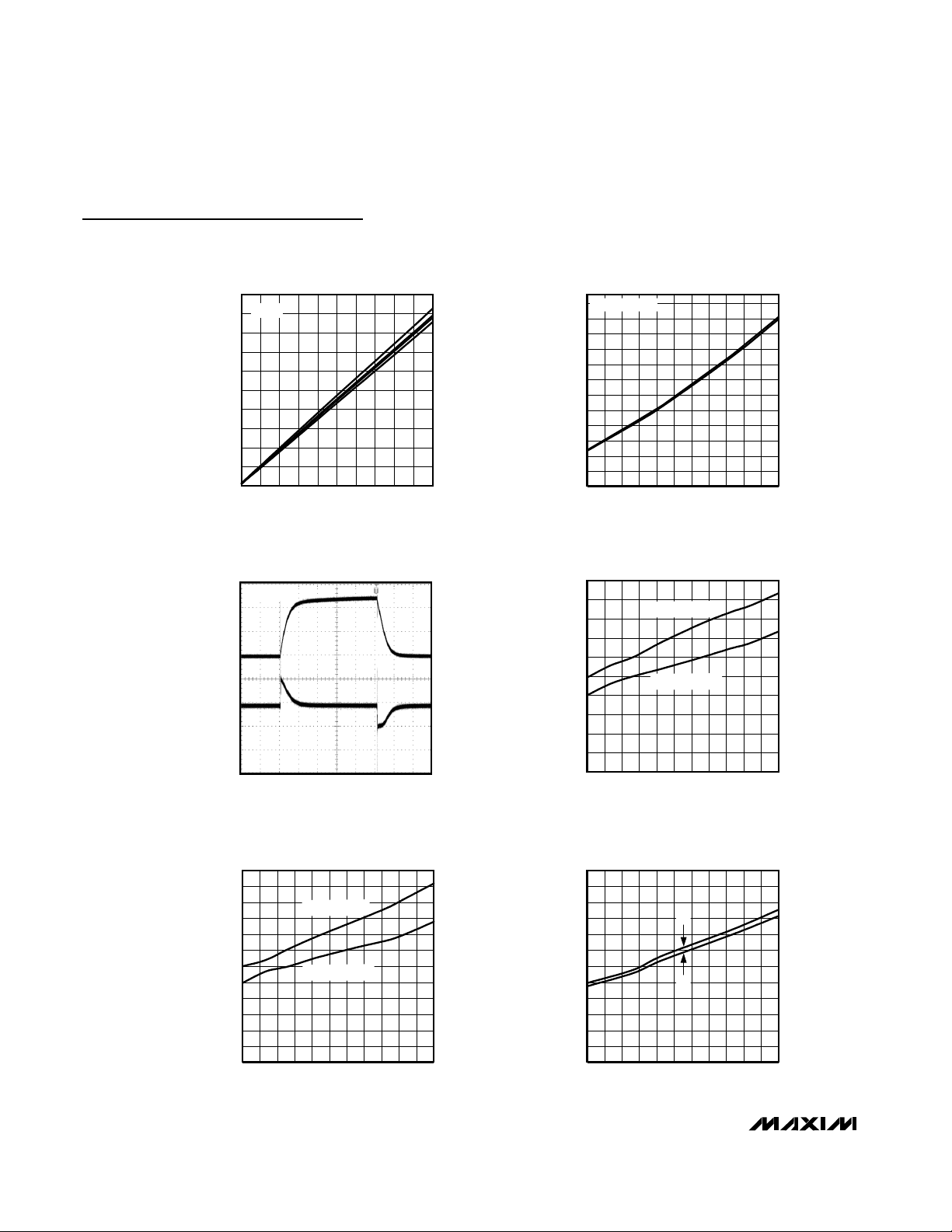
6 _______________________________________________________________________________________
VDD AND BST OPERATING SUPPLY
CURRENT vs. FREQUENCY
MAX5062/3/4 toc08
FREQUENCY (kHz)
I
DDO
+ I
BSTO
(mA)
900700 800200 300 400 500 600100
1
2
3
4
5
6
7
8
9
10
0
0 1000
CL = 0
DH OR DL OUTPUT LOW VOLTAGE
vs. TEMPERATURE
MAX5062/3/4 toc09
TEMPERATURE (°C)
OUTPUT LOW VOLTAGE (V)
1109565 80-10 5 20 35 50-25
0.12
0.14
0.16
0.18
0.20
0.24
0.28
0.32
0.34
0.22
0.26
0.30
0.10
-40 125
SINKING 100mA
DH OR DL FALL TIME
vs. TEMPERATURE (C
LOAD
= 10nF)
MAX5062/3/4 toc12
TEMPERATURE (°C)
t
F
(ns)
1109565 80-10 5 20 35 50-25
10
20
30
40
50
70
110
100
90
120
60
80
0
-40 125
VDD = V
BST
= 8V
VDD = V
BST
= 12V
DH OR DL RISE PROPAGATION DELAY
vs. TEMPERATURE
MAX5062/3/4 toc13
TEMPERATURE (°C)
PROPAGATION DELAY (ns)
1109565 80-10 5 20 35 50-25
5
10
15
20
25
35
55
60
30
45
50
40
0
-40 125
DH
DL
PEAK DH AND DL
SOURCE/SINK CURRENT
MAX5062/3/4 toc10
1µs/div
DH OR DL5V/div
SINK AND SOURCE
CURRENT
2A/div
CL = 100nF
DH OR DL RISE TIME
vs. TEMPERATURE (C
L
= 10nF)
MAX5062/3/4 toc11
TEMPERATURE (°C)
t
R
(ns)
1109565 80-10 5 20 35 50-25
12
24
36
48
60
84
108
120
72
96
0
-40 125
VDD = V
BST
= 8V
VDD = V
BST
= 12V
Typical Operating Characteristics (continued)
(Typical values are at VDD= V
BST
= +12V and TA= +25°C, unless otherwise specified.)
Page 7

MAX5062/MAX5063/MAX5064
125V/2A, High-Speed,
Half-Bridge MOSFET Drivers
_______________________________________________________________________________________ 7
DH OR DL FALL PROPAGATION DELAY
vs. TEMPERATURE
MAX5062/3/4 toc14
TEMPERATURE (°C)
PROPAGATION DELAY (ns)
1109565 80-10 5 20 35 50-25
5
10
15
20
25
35
55
60
30
45
50
40
0
-40 125
DH
DL
BREAK-BEFORE-MAKE
DEAD TIME vs. R
BBM
MAX5062/3/4 toc15
R
BBM
(kΩ)
t
BBM
(ns)
290
210 25090 130
170
50
25
50
75
100
125
175
250
150
200
225
0
10
MAX5064
BREAK-BEFORE-MAKE DEAD TIME
vs. TEMPERATURE
MAX5062/3/4 toc16
TEMPERATURE (°C)
t
BBM
(ns)
1109565 80-10 5 20 35 50-25
10
20
30
40
50
70
110
100
90
120
60
80
0
-40 125
R
BBM
= 100kΩ
R
BBM
= 10kΩ
MAX5064
DELAY MATCHING (DH/DL RISING)
MAX5062/3/4 toc17
10ns/div
INPUT
5V/div
5V/div
DH/DL
CL = 0
DELAY MATCHING (DH/DL FALLING)
MAX5062/3/4 toc18
10ns/div
INPUT
5V/div
5V/div
DH/DL
CL = 0
DH/DL RESPONSE TO VDD GLITCH
MAX5062/3/4 toc19
40µs/div
DH
DL
V
DD
10V/div
10V/div
10V/div
5V/div
INPUT
Typical Operating Characteristics (continued)
(Typical values are at VDD= V
BST
= +12V and TA= +25°C, unless otherwise specified.)
Page 8

MAX5062/MAX5063/MAX5064
125V/2A, High-Speed,
Half-Bridge MOSFET Drivers
8 _______________________________________________________________________________________
PIN NAME FUNCTION
1 BST
Boost Flying Capacitor Connection. Connect a 0.1µF ceramic capacitor between BST and HS for the
high-side MOSFET driver supply.
2 DH High-Side-Gate Driver Output. Drives high-side MOSFET gate.
3 HS Source Connection for High-Side MOSFET. Also serves as a return terminal for the high-side driver.
4 AGND
Analog Ground. Return path for low-switching current signals. IN_H/IN_L inputs referenced to
5 BBM
Break-Before-Make Programming Resistor Connection. Connect a 10kΩ to 100kΩ resistor from BBM
to AGND to program the break-before-make time (t
BBM
) from 16ns to 95ns. Resistance values
greater than 200kΩ disables the BBM function and makes t
BBM
= 1ns. Bypass this pin with at least a
1nF capacitor to AGND.
6 IN_H-
High-Side Inverting CMOS (V
DD
/ 2) (MAX5064A), or TTL (MAX5064B) Logic Input. Connect to
AGND when not used.
7 IN_H+
High-Side Noninverting CMOS (V
DD
/ 2) (MAX5064A), or TTL (MAX5064B) Logic Input. Connect to
V
DD
when not used.
8 IN_L-
Low-Side Inverting CMOS (V
DD
/ 2) (MAX5064A), or TTL (MAX5064B) Logic Input. Connect to AGND
when not used.
9 IN_L+
Low-Side Noninverting CMOS (V
DD
/ 2) (MAX5064A), or TTL (MAX5064B) Logic Input. Connect to
V
DD
when not used.
10 PGND
Power Ground. Return path for high-switching current signals. Use PGND as a return path for the
low-side driver.
11 DL Low-Side-Gate Driver Output. Drives the low-side MOSFET gate.
12 V
DD
Power Input. Bypass to PGND with a 0.1µF ceramic in parallel with a 1µF ceramic capacitor.
— EP
Exposed Pad. Internally connected to AGND. Externally connect to a large ground plane to aid in
heat dissipation.
MAX5064 Pin Description
PIN NAME FUNCTION
1VDDPower Input. Bypass to GND with a parallel combination of 0.1µF and 1µF ceramic capacitor.
2 BST
Boost Flying Capacitor Connection. Connect a 0.1µF ceramic capacitor between BST and HS for the
high-side MOSFET driver supply.
3 DH High-Side-Gate Driver Output. Driver output for the high-side MOSFET gate.
4 HS Source Connection for High-Side MOSFET. Also serves as a return terminal for the high-side driver.
5 IN_H High-Side Noninverting Logic Input
6 IN_L
Low-Side Noninverting Logic Input (MAX5062A/C, MAX5063A/C). Low-side inverting logic input
(MAX5062B/D, MAX5063B/D).
7 GND Ground. Use GND as a return path to the DL driver output and IN_H/IN_L inputs.
8 DL Low-Side-Gate Driver Output. Drives low-side MOSFET gate.
— EP
Exposed Pad. Internally connected to GND. Externally connect the exposed pad to a large ground
plane to aid in heat dissipation (MAX5062C/D, MAX5063C/D only).
MAX5062/MAX5063 Pin Description
Page 9

MAX5062/MAX5063/MAX5064
125V/2A, High-Speed,
Half-Bridge MOSFET Drivers
_______________________________________________________________________________________ 9
Detailed Description
The MAX5062/MAX5063/MAX5064 are 125V/2A highspeed, half-bridge MOSFET drivers that operate from a
supply voltage of +8V to +12.6V. The drivers are
intended to drive a high-side switch without any isolation device like an optocoupler or drive transformer.
The high-side driver is controlled by a TTL/CMOS logic
signal referenced to ground. The 2A source and sink
drive capability is achieved by using low R
DS_ON
pand n-channel driver output stages. The BiCMOS
process allows extremely fast rise/fall times and low
propagation delays. The typical propagation delay from
the logic-input signal to the drive output is 35ns with a
matched propagation delay of 3ns typical. Matching
these propagation delays is as important as the
absolute value of the delay itself. The high 125V input
voltage range allows plenty of margin above the 100V
transient specification per telecom standards.
The MAX5064 is available in a thermally enhanced
TQFN package, which can dissipate up to 1.95W (at
+70°C) and allow up to 1MHz switching frequency
while driving 100nC combined gate-charge MOSFETs.
Figure 1. Timing Characteristics for Noninverting and Inverting Logic Inputs
V
IH
V
IL
90%
10%
V
IH
V
IL
t
F
IN_H+
DH
IN_H-
t
D_ON3
t
D_ON4
t
D_OFF4
t
D_OFF3
V
IH
V
IL
90%
10%
V
IH
V
IL
t
R
t
R
t
F
IN_L+
DL
IN_L-
t
D_ON1
t
D_ON2
t
D_OFF2
t
D_OFF1
t
MATCH1
= (t
D_ON2
- t
D_ON1
) or (t
D_OFF2
- t
D_OFF1
)
t
MATCH2
= (t
D_ON3
- t
D_ON1
) or (t
D_ON4
- t
D_ON2
) or (t
D_OFF3
- t
D_OFF1
) or (t
D_OFF4
- t
D_OFF2
)
Page 10

MAX5062/MAX5063/MAX5064
Undervoltage Lockout
Both the high- and low-side drivers feature undervoltage lockout (UVLO). The low-side driver’s UVLO
LOW
threshold is referenced to GND and pulls both driver
outputs low when VDDfalls below 6.8V. The high-side
driver has its own undervoltage lockout threshold
(UVLO
HIGH
), referenced to HS, and pulls DH low when
BST falls below 6.4V with respect to HS.
During turn-on, once VDDrises above its UVLO threshold, DL starts switching and follows the IN_L logic input.
At this time, the bootstrap capacitor is not charged and
the BST-to-HS voltage is below UVLO
BST
. For synchronous buck and half-bridge converter topologies, the
bootstrap capacitor can charge up in one cycle and
normal operation begins in a few microseconds after the
BST-to-HS voltage exceeds UVLO
BST
. In the two-switch
forward topology, the BST capacitor takes some time (a
few hundred microseconds) to charge and increase its
voltage above UVLO
BST
.
The typical hysteresis for both UVLO thresholds is 0.5V.
The bootstrap capacitor value should be selected carefully to avoid unintentional oscillations during turn-on
and turn-off at the DH output. Choose the capacitor
value about 20 times higher than the total gate capacitance of the MOSFET. Use a low-ESR-type X7R dielectric ceramic capacitor at BST (typically a 0.1µF ceramic
is adequate) and a parallel combination of 1µF and
0.1µF ceramic capacitors from V
DD
to GND
(MAX5062_, MAX5063_) or to PGND (MAX5064_). The
high-side MOSFET’s continuous on-time is limited due
to the charge loss from the high-side driver’s quiescent
current. The maximum on-time is dependent on the size
of C
BST
, I
BST
(50µA max), and UVLO
BST
.
Output Driver
The MAX5062/MAX5063/MAX5064 have low 2.5Ω
R
DS_ON
p-channel and n-channel devices (totem pole)
in the output stage. This allows for a fast turn-on and
turn-off of the high gate-charge switching MOSFETs.
The peak source and sink current is typically 2A.
Propagation delays from the logic inputs to the driver
outputs are matched to within 8ns. The internal p- and
n-channel MOSFETs have a 1ns break-before-make
logic to avoid any cross conduction between them. This
internal break-before-make logic eliminates shootthrough currents reducing the operating supply current
as well as the spikes at VDD. The DL voltage is approximately equal to VDDand the DH-to-HS voltage, a diode
drop below VDD, when they are in a high state and to
zero when in a low state. The driver R
DS_ON
is lower at
higher VDD. Lower R
DS_ON
means higher source and
sink currents and faster switching speeds.
Internal Bootstrap Diode
An internal diode connects from VDDto BST and is
used in conjunction with a bootstrap capacitor externally connected between BST and HS. The diode charges
the capacitor from VDDwhen the DL low-side switch is
on and isolates VDDwhen HS is pulled high as the highside driver turns on (see the Typical Operating Circuit).
The internal bootstrap diode has a typical forward voltage drop of 0.9V and has a 10ns typical turn-off/turn-on
time. For lower voltage drops from VDDto BST, connect
an external Schottky diode between VDDand BST.
Programmable Break-Before-Make
(MAX5064)
Half-bridge and synchronous buck topologies require
that the high- or low-side switch be turned off before
the other switch is turned on to avoid shoot-through
currents. Shoot-through occurs when both high- and
low-side switches are on at the same time. This condition is caused by the mismatch in the propagation
delay from IN_H/IN_L to DH/DL, driver output impedance, and the MOSFET gate capacitance. Shootthrough currents increase power dissipation, radiate
EMI, and can be catastrophic, especially with high
input voltages.
The MAX5064 offers a break-before-make (BBM) feature that allows the adjustment of the delay from the
input to the output of each driver. The propagation
delay from the rising edges of IN_H and IN_L to the rising edges of DH and DL, respectively, can be programmed from 16ns to 95ns. Note that the BBM time
(t
BBM
) has a higher percentage error at lower value
because of the fixed comparator delay in the BBM
block. The propagation delay mismatch (t
MATCH_
)
needs to be included when calculating the total t
BBM
error. The low 8ns (maximum) delay mismatch reduces
the total t
BBM
variation. Use the following equations to
calculate R
BBM
for the required BBM time and
t
BBM_ERROR
:
where t
BBM
is in nanoseconds.
Rk
t
ns
for R k
ttt
BBM
BBM
BBM
BBM ERROR BBM MATCH
.
__
=×
<
=× +
−10
8
1 200
015
ΩΩ
125V/2A, High-Speed,
Half-Bridge MOSFET Drivers
10 ______________________________________________________________________________________
Page 11

The voltage at BBM is regulated to 1.3V. The BBM circuit
adjusts t
BBM
depending on the current drawn by R
BBM
.
Bypass BBM to AGND with a 1nF or smaller ceramic
capacitor (C
BBM
) to avoid any effect of ground bounce
caused during switching. The charging time of C
BBM
does not affect t
BBM
at turn-on because the BBM voltage
is stabilized before the UVLO clears the device turn-on.
Topologies like the two-switch forward converter, where
both high- and low-side switches are turned on and off
simultaneously, can have the BBM function disabled by
leaving BBM unconnected. When disabled, t
BBM
is typi-
cally 1ns.
Driver Logic Inputs (IN_H, IN_L, IN_H+,
IN_H-, IN_L+, IN_L-)
The MAX5062_/MAX5064A are CMOS (V
DD
/ 2) logicinput drivers while the MAX5063_/MAX5064B have TTLcompatible logic inputs. The logic-input signals are
independent of VDD. For example, the IC can be powered by a 10V supply while the logic inputs are provided from a 12V CMOS logic. Also, the logic inputs are
protected against voltage spikes up to 15V, regardless
of the VDDvoltage. The TTL and CMOS logic inputs
have 400mV and 1.6V hysteresis, respectively, to avoid
double pulsing during transition. The logic inputs are
high-impedance pins and should not be left floating.
The low 2.5pF input capacitance reduces loading and
increases switching speed. The noninverting inputs are
pulled down to GND and the inverting inputs are pulled
up to V
DD
internally using a 1MΩ resistor. The PWM
output from the controller must assume a proper state
while powering up the device. With the logic inputs
floating, the DH and DL outputs pull low as V
DD
rises
up above the UVLO threshold.
The MAX5064_ has two logic inputs per driver, which
provide greater flexibility in controlling the MOSFET.
Use IN_H+/IN_L+ for noninverting logic and IN_H-/
IN_L- for inverting logic operation. Connect
IN_H+/IN_L+ to V
DD
and IN_H-/IN_L- to GND if not
used. Alternatively, the unused input can be used as an
ON/OFF function. Use IN_+ for active-low and IN_- for
active-high shutdown logic.
Table 1. MAX5064_ Truth Table
Applications Information
Supply Bypassing and Grounding
Pay extra attention to bypassing and grounding the
MAX5062/MAX5063/MAX5064. Peak supply and output
currents may exceed 4A when both drivers are driving
large external capacitive loads in-phase. Supply drops
and ground shifts create forms of negative feedback for
inverters and may degrade the delay and transition
times. Ground shifts due to insufficient device grounding may also disturb other circuits sharing the same AC
ground return path. Any series inductance in the V
DD
,
DH, DL, and/or GND paths can cause oscillations due
to the very high di/dt when switching the MAX5062/
MAX5063/MAX5064 with any capacitive load. Place
one or more 0.1µF ceramic capacitors in parallel as
close to the device as possible to bypass VDDto GND
(MAX5062/MAX5063) or PGND (MAX5064). Use a
ground plane to minimize ground return resistance and
series inductance. Place the external MOSFET as close
as possible to the MAX5062/MAX5063/MAX5064 to further minimize board inductance and AC path resistance. For the MAX5064_ the low-power logic ground
(AGND) is separated from the high-power driver return
(PGND). Apply the logic-input signal between IN_ to
AGND and connect the load (MOSFET gate) between
DL and PGND.
Power Dissipation
Power dissipation in the MAX5062/MAX5063/MAX5064
is primarily due to power loss in the internal boost
diode and the nMOS and pMOS FETS.
For capacitive loads, the total power dissipation for the
device is:
where CLis the combined capacitive load at DH and
DL. V
DD
is the supply voltage and fSWis the switching
frequency of the converter. P
D
includes the power dissipated in the internal bootstrap diode. The internal
power dissipation reduces by P
DIODE
, if an external
bootstrap Schottky diode is used. The power dissipation in the internal boost diode (when driving a capacitive load) will be the charge through the diode per
switching period multiplied by the maximum diode forward voltage drop (Vf= 1V).
PCV fV
DIODE DH DD SW f
=×
()
××− 1
PCV f I I V
D L DD SW DDO BSTO DD
=× ×
++
()
×
2
MAX5062/MAX5063/MAX5064
125V/2A, High-Speed,
Half-Bridge MOSFET Drivers
______________________________________________________________________________________ 11
IN_H+/IN_L+ IN_H-/IN_L- DH/DL
Low Low Low
Low High Low
High Low High
High High Low
Page 12

MAX5062/MAX5063/MAX5064
The total power dissipation when using the internal
boost diode will be PDand, when using an external
Schottky diode, will be PD- P
DIODE
. The total power
dissipated in the device must be kept below the maximum of 1.951W for the 12-pin TQFN package, 1.5W for
the 8-pin SO with exposed pad, and 0.471W for the
regular 8-pin SO package at TA= +70°C ambient.
Layout Information
The MAX5062/MAX5063/MAX5064 drivers source and
sink large currents to create very fast rise and fall
edges at the gates of the switching MOSFETs. The high
di/dt can cause unacceptable ringing if the trace
lengths and impedances are not well controlled. Use
the following PC board layout guidelines when designing with the MAX5062/MAX5063/MAX5064:
• It is important that the VDDvoltage (with respect to
ground) or BST voltage (with respect to HS) does
not exceed 13.2V. Voltage spikes higher than 13.2V
from VDDto GND or BST to HS can damage the
device. Place one or more low ESL 0.1µF decoupling ceramic capacitors from V
DD
to GND
(MAX5062/MAX5063) or to PGND (MAX5064), and
from BST to HS as close as possible to the part. The
ceramic decoupling capacitors should be at least 20
times the gate capacitance being driven.
• There are two AC current loops formed between the
device and the gate of the MOSFET being driven.
The MOSFET looks like a large capacitance from gate
to source when the gate is being pulled low. The
active current loop is from the MOSFET driver output
(DL or DH) to the MOSFET gate, to the MOSFET
source, and to the return terminal of the MOSFET driver (either GND or HS). When the gate of the MOSFET
is being pulled high, the active current loop is from
the MOSFET driver output, (DL or DH), to the
MOSFET gate, to the MOSFET source, to the return
terminal of the drivers decoupling capacitor, to the
positive terminal of the decoupling capacitor, and to
the supply connection of the MOSFET driver. The
decoupling capacitor will be either the flying capacitor
connected between BST and HS or the decoupling
capacitor for V
DD
. Care must be taken to minimize the
physical distance and the impedance of these AC
current paths.
• Solder the exposed pad of the TQFN (MAX5064) or
SO (MAX5062C/D and MAX5063C/D) package to a
large copper plane to achieve the rated power dissipation. Connect AGND and PGND at one point near
VDD’s decoupling capacitor return.
125V/2A, High-Speed,
Half-Bridge MOSFET Drivers
12 ______________________________________________________________________________________
Page 13
MAX5062/MAX5063/MAX5064
125V/2A, High-Speed,
Half-Bridge MOSFET Drivers
______________________________________________________________________________________ 13
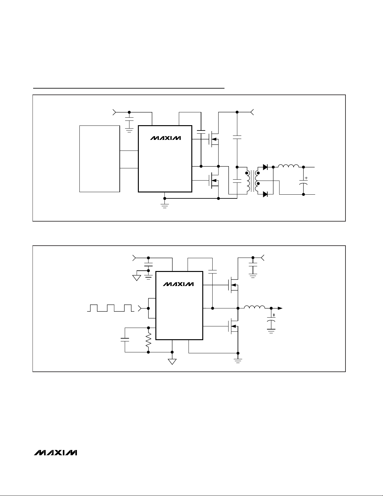
Typical Application Circuits
Figure 2. MAX5062 Half-Bridge Conversion
MAX5062A/
MAX5063A
V
OUT
N
N
V
DD
= 8V TO 12.6V
V
IN
= 0 TO 125V
V
DD
BST
IN_H
IN_L
GND
DL
DH
HS
PWM
CONTROLLER
PIN FOR PIN REPLACEMENT FOR THE HIP2100/HIP2101
Figure 3. Synchronous Buck Converter
MAX5064
N
N
V
DD
= 8V TO 12.6V
V
IN
= 0 TO 125V
V
OUT
V
DD
BST
IN_H+
IN_L-
BBM
AGND PGND
DL
DH
HS
R
BBM
PWM
C
BBM
C
BST
Page 14

MAX5062/MAX5063/MAX5064
125V/2A, High-Speed,
Half-Bridge MOSFET Drivers
14 ______________________________________________________________________________________
Typical Application Circuits (continued)
Figure 4. Two-Switch Forward Conversion
MAX5064
N
N
V
DD
= 8V TO 12.6V
V
IN
= 0 TO 125V
V
OUT
V
DD
BST
IN_H+
IN_L+
BBM
AGND PGND
DL
DH
HS
PWM
C
BST
Figure 5. MAX5064 Half-Bridge Converter
MAX5064_
V
OUT
N
N
V
DD
= 8V TO 12.6V
V
IN
= 0 TO 125V
V
DD
BST
IN_H+
IN_L-
BBM
PGNDAGND
DL
DH
HS
R
BBM
PWM
C
BBM
C
BST
Page 15

MAX5062/MAX5063/MAX5064
125V/2A, High-Speed,
Half-Bridge MOSFET Drivers
______________________________________________________________________________________ 15
IN_L
IN_HHS
1
2
87DL
GNDBST
DH
V
DD
SO
TOP VIEW
3
4
6
5
MAX5062A/B
MAX5063A/B
IN_L
IN_HHS
1
2
87DL
GNDBST
DH
V
DD
SO-EP
3
4
6
5
MAX5062C/D
MAX5063C/D
9
IN_L+8IN_L-7IN_H+
12DH3
HS
10
11DL
12
6
5
4V
DD
IN_H-
BBM
AGND
MAX5064A/
MAX5064B
PGND
BST
THIN QFN
Pin Configurations
MAX5062A
MAX5062C
GND
V
DD
IN_H
DH
DL
HS
BST
IN_L
2
3
4
5
8
7
6
1
V
DD
/2 CMOS
MAX5064A
PGND
V
DD
IN_H+
IN_L-
DH
DL
HS
BST
BBM
IN_H-
IN_L+
AGND
1
2
4
3
7
8
5
6
11
10
9
12
V
DD
/2 CMOS
MAX5064B
PGND
V
DD
IN_H+
IN_L-
DH
DL
HS
BST
BBM
IN_H-
IN_L+
AGND
1
2
4
3
7
8
5
6
11
10
9
12
TTL
SO/SO-EP
MAX5062B/
MAX5062D
GND
V
DD
IN_H
DH
DL
HS
BST
IN_L
2
3
4
5
8
7
6
1
V
DD
/2 CMOS
SO/SO-EP
MAX5063B/
MAX5063D
GND
V
DD
IN_H
DH
DL
HS
BST
IN_L
2
3
4
5
8
7
6
1
TTL
SO/SO-EP
MAX5063A/
MAX5063C
GND
V
DD
IN_H
DH
DL
HS
BST
IN_L
2
3
4
5
8
7
6
1
TTL
SO/SO-EP
THIN QFN THIN QFN
Functional Diagrams
Page 16

MAX5062/MAX5063/MAX5064
125V/2A, High-Speed,
Half-Bridge MOSFET Drivers
16 ______________________________________________________________________________________
MAX5064A/
MAX5064B
PWM IN
V
OUT
PGND
IN_H+
IN_L-
DH
DL
HS
BST
BBM
V
DD
IN_L+
IN_H-
R
BBM
AGND
C
BBM
V
DD
C
BST
C
DD
VIN = 125V
V
DD
8V TO 12.6V
Typical Operating Circuit
PART TEMP RANGE
PIN-
TOP
MARK
MAX5063AASA
8 SO —
MAX5063BASA
8 SO —
MAX5063CASA
8 SO-EP* —
MAX5063DASA
8 SO-EP* —
MAX5064AATC
12 TQFN
AAEF
MAX5064BATC
12 TQFN
AAEG
Ordering Information (continued)
PART HIGH-SIDE DRIVER LOW-SIDE DRIVER LOGIC LEVELS PIN COMPATIBLE
MAX5063AASA Noninverting Noninverting TTL HIP2101IB
MAX5063BASA Noninverting Inverting TTL —
MAX5063CASA Noninverting Noninverting TTL —
MAX5063DASA Noninverting Inverting TTL —
MAX5064AATC
Both Inverting and
Noninverting
Both Inverting and
Noninverting
CMOS (V
DD
/ 2) —
MAX5064BATC
Both Inverting and
Noninverting
Both Inverting and
Noninverting
TTL —
Selector Guide (continued)
Chip Information
TRANSISTOR COUNT: 790
PROCESS: HV BiCMOS
*EP = Exposed paddle.
PACKAGE
-40°C to +125°C
-40°C to +125°C
-40°C to +125°C
-40°C to +125°C
-40°C to +125°C
-40°C to +125°C
Page 17

MAX5062/MAX5063/MAX5064
125V/2A, High-Speed,
Half-Bridge MOSFET Drivers
______________________________________________________________________________________ 17
Package Information
(The package drawing(s) in this data sheet may not reflect the most current specifications. For the latest package outline information
go to www.maxim-ic.com/packages
.)
8L, SOIC EXP. PAD.EPS
B
1
1
21-0111
PACKAGE OUTLINE
8L SOIC, .150" EXPOSED PAD
Page 18

MAX5062/MAX5063/MAX5064
125V/2A, High-Speed,
Half-Bridge MOSFET Drivers
18 ______________________________________________________________________________________
Package Information (continued)
(The package drawing(s) in this data sheet may not reflect the most current specifications. For the latest package outline information
go to www.maxim-ic.com/packages
.)
12,16,20, 24L QFN.EPS
E
1
2
21-0106
PACKAGE OUTLINE
12,16,20,24L QFN, 4x4x0.90 MM
Page 19

MAX5062/MAX5063/MAX5064
125V/2A, High-Speed,
Half-Bridge MOSFET Drivers
Maxim cannot assume responsibility for use of any circuitry other than circuitry entirely embodied in a Maxim product. No circuit patent licenses are
implied. Maxim reserves the right to change the circuitry and specifications without notice at any time.
Maxim Integrated Products, 120 San Gabriel Drive, Sunnyvale, CA 94086 408-737-7600 ____________________ 19
© 2005 Maxim Integrated Products Printed USA is a registered trademark of Maxim Integrated Products, Inc.
Package Information (continued)
(The package drawing(s) in this data sheet may not reflect the most current specifications. For the latest package outline information
go to www.maxim-ic.com/packages
.)
E
2
2
21-0106
PACKAGE OUTLINE
12,16,20,24L QFN, 4x4x0.90 MM
 Loading...