

Page 1

General Description
The MAX5051 is a clamped, two-switch power-supply
controller IC. This device can be used both in forward or
flyback configurations with input voltage ranges from 11V
to 76V. It provides comprehensive protection mechanisms against possible faults, resulting in very high reliability power supplies. When used in conjunction with secondary-side synchronous rectification, power-supply
efficiencies can easily reach 92% for a +3.3V output
power supply operated from a 48V bus. The integrated
high- and low-side gate drivers provide more than 2A of
peak gate-drive current to two external N-channel
MOSFETs. Low startup current reduces the power loss
across the bootstrap resistor. A feed-forward voltagemode topology provides excellent line rejection while
avoiding the pitfalls of traditional current-mode control.
The MAX5051 power-supply controller is primary as
well as secondary-side parallelable, allowing the
design of scaleable power systems when necessary.
When paralleling the primary side, dedicated pins allow
for simultaneous wakeup or shutdown of all paralleled
units, thus preventing current-hogging during startup or
fault conditions.
The MAX5051 generates a lookahead signal for driving
secondary-side synchronous MOSFETs. Special
primary-side synchronization inputs/outputs allow two
primaries to be operated 180° out of phase for increased
output power and lower input ripple currents.
The MAX5051 is available in a 28-pin TSSOP-EP
package and operates over a wide -40°C to +125°C
temperature range.
Warning: The MAX5051 is designed to work with
high voltages. Exercise caution.
Applications
High-Efficiency, Isolated Telecom/Datacom
Power Supplies
48V and 12V Server Power Supplies
48V Power-Supply Modules
42V Automotive Power Systems
Industrial Power Supplies
Features
♦ Wide Input Voltage Range, 11V to 76V
♦ Voltage Mode with Input Voltage Feed-Forward
♦ Ripple-Phased Parallel Topology for High
Current/Power Output
♦ 2A Integrated High- and Low-Side MOSFET
Drivers
♦ SYNCIN And SYNCOUT Pins Enable 180° Out-Of-
Phase Operation
♦ Programmable Brownout and Bootstrap UVLOs
♦ High-Side Driver Bootstrap Capacitor Precharge
Driver
♦ Low Current-Limit Threshold for High Efficiency
♦ Programmable Switching Frequency
♦ Reference Voltage Soft-Start for Startup Without
Overshoots
♦ Startup Synchronization with Multiple Paralleled
Primaries
♦ Programmable Integrating Current-Limit Fault
Protection
♦ Look-Ahead PWM Signal for Secondary-Side
Synchronous Rectifier Drivers
♦ Look-Ahead Drivers for Either A High-Speed
Optocoupler or Pulse Transformer
♦ Wide -40°C to +125°C Operating Range
♦ Thermally Enhanced 28-Pin TSSOP Package
MAX5051
Parallelable, Clamped Two-Switch
Power-Supply Controller IC
________________________________________________________________ Maxim Integrated Products 1
Ordering Information
19-2964; Rev 0; 8/03
For pricing, delivery, and ordering information, please contact Maxim/Dallas Direct! at
1-888-629-4642, or visit Maxim’s website at www.maxim-ic.com.
EVALUATION KIT
AVAILABLE
*EP = Exposed pad.
Pin Configuration appears at end of data sheet.
PART TEMP RANGE PIN-PACKAGE
MAX5051AUI -40°C to +125°C 28-TSSOP-EP*
Page 2
MAX5051
Parallelable, Clamped Two-Switch
Power-Supply Controller IC
2 _______________________________________________________________________________________
ABSOLUTE MAXIMUM RATINGS
ELECTRICAL CHARACTERISTICS
(AVIN = 12V, PVIN = 12V, V
UVLO
= V
STT
= 3V, V
CON
= 3V, R
RCOSC
= 24kΩ, C
CSS
= 10nF, C
RCOSC
= 100pF, C
REG9
= 4.7µF,
C
REG5
= 4.7µF, TA= T
MIN
to T
MAX
, unless otherwise noted. Typical values are at TA= +25°C. All driver, voltage-regulator, and refer-
ence outputs unconnected except for bypass capacitors.)
Stresses beyond those listed under “Absolute Maximum Ratings” may cause permanent damage to the device. These are stress ratings only, and functional
operation of the device at these or any other conditions beyond those indicated in the operational sections of the specifications is not implied. Exposure to
absolute maximum rating conditions for extended periods may affect device reliability.
AVIN, PVIN, XFRMRH to GND................................-0.3V to +80V
BST to GND ............................................................-0.3V to +95V
BST, DRVH to XFRMRH..........................................-0.3V to +12V
REG9, DRVDD, DRVL to GND................................-0.3V to +12V
DRVB, LXVDD, LXL, LXH to GND ..........................-0.3V to +12V
UVLO, STT, COMP, CON to GND ..........................-0.3V to +12V
FLTINT, RCFF to GND ............................................-0.3V to +12V
REG5, CS, CSS, FB to GND .....................................-0.3V to +6V
STARTUP, SYNCIN to GND......................................-0.3V to +6V
SYNCOUT, RCOSC to GND .....................................-0.3V to +6V
PGND to GND .......................................................-0.3V to +0.3V
LXL, LXH Current Continuous...........................................±50mA
DRVL, DRVH Current Continuous...................................±100mA
DRVL, DRVH Peak Current (<500ns) ....................................±5A
PVIN, REG9 Continuous Current ....................................+120mA
REG5 Continuous Current ................................................+80mA
DRVB, RCFF, RCOSC, CSS Continuous Current .............±20mA
COMP, SYNCOUT Continuous Current ............................±20mA
REG9, REG5, and COMP Short to GND ....................Continuous
Continuous Power Dissipation (T
A
= +70°C)
28-Pin TSSOP (derate 23.8mW/°C above +70°C) .....1905mW
28-Pin TSSOP (θ
JA
)......................................................42°C/W
Operating Temperature Range .........................-40°C to +125°C
Maximum Junction Temperature (T
J
) ..............................+150°C
Storage Temperature Range .............................-65°C to +150°C
Lead Temperature (soldering, 10s) .................................+300°C
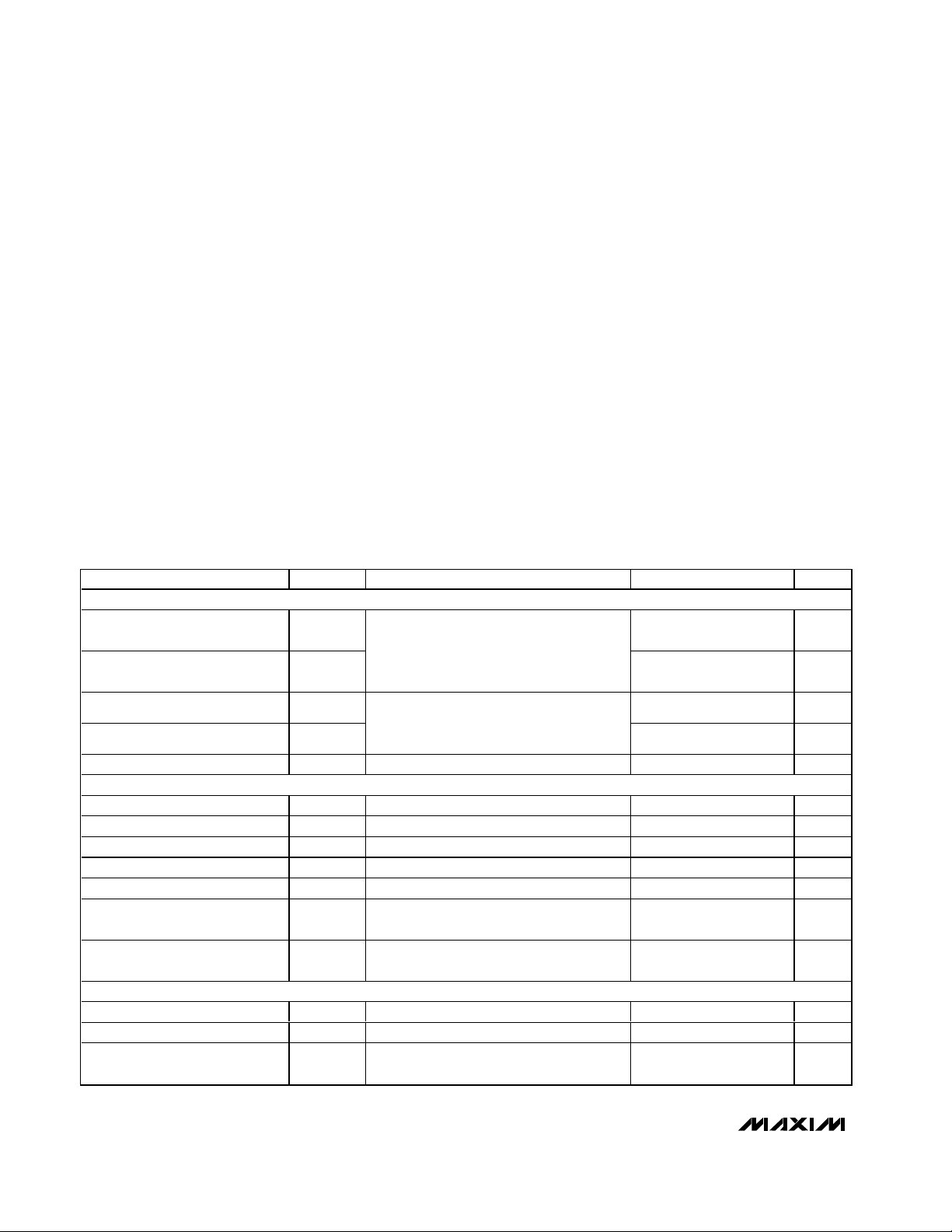
PARAMETER SYMBOL CONDITIONS MIN TYP MAX UNITS
SUPPLY CURRENT (AVIN, PVIN)
AVIN Standby Current I
PVIN Standby Current I
AVIN Supply Current I
PVIN Supply Current I
ASTBY
PSTBY
AVIN
PVIN
= V
AVIN
V
STARTUP
V
= V
BST
RCFF floating
V
= V
AVIN
= V
V
BST
STARTUP, RCFF floating
= 11V to 76V;
PVIN
= V
= 0V;
CS
= V
XFRMRH
PVIN
DRVDD
DRVDD
= 11V to 76V; VCS = 0V;
= V
REG9
; V
= V
REG9
XFRMRH
;
= 0V;
300 450 µA
400 650 µA
0.65 1 mA
812mA
V
AVIN Input Voltage Range Inferred from AVIN supply current test 11 76 V
+9V LDO (REG9)
PVIN Input Voltage Range V
REG9 Output-Voltage Set Point V
PVIN
REG9
REG9 Line Regulation V
REG9 Load Regulation I
REG9 Dropout Voltage I
REG9 Undervoltage Lockout
Threshold
REG9 Undervoltage Lockout
Threshold Hysteresis
Inferred from PVIN supply current test 11 76 V
V
= 11V 8.3 9.0 V
PVIN
= 11V to 76V 0.1 mV/V
PVIN
= 0 to 80mA 250 mV
REG9
= 80mA 0.5 V
REG9
V
falling 5.7 6.7 V
REG9
750 mV
+5V LDO (REG5)
REG5 Output-Voltage Set Point V
REG5
REG5 Load Regulation I
REG5 Dropout Voltage
= 0 to 40mA 50 mV
REG5
I
= 40mA, measured with respect
REG5
to V
REG9
4.8 5.1 V
0.5 V
Page 3
MAX5051
Parallelable, Clamped Two-Switch
Power-Supply Controller IC
_______________________________________________________________________________________ 3
ELECTRICAL CHARACTERISTICS (continued)
(AVIN = 12V, PVIN = 12V, V
UVLO
= V
STT
= 3V, V
CON
= 3V, R
RCOSC
= 24kΩ, C
CSS
= 10nF, C
RCOSC
= 100pF, C
REG9
= 4.7µF,
C
REG5
= 4.7µF, TA= T
MIN
to T
MAX
, unless otherwise noted. Typical values are at TA= +25°C. All driver, voltage-regulator, and refer-
ence outputs unconnected except for bypass capacitors.)
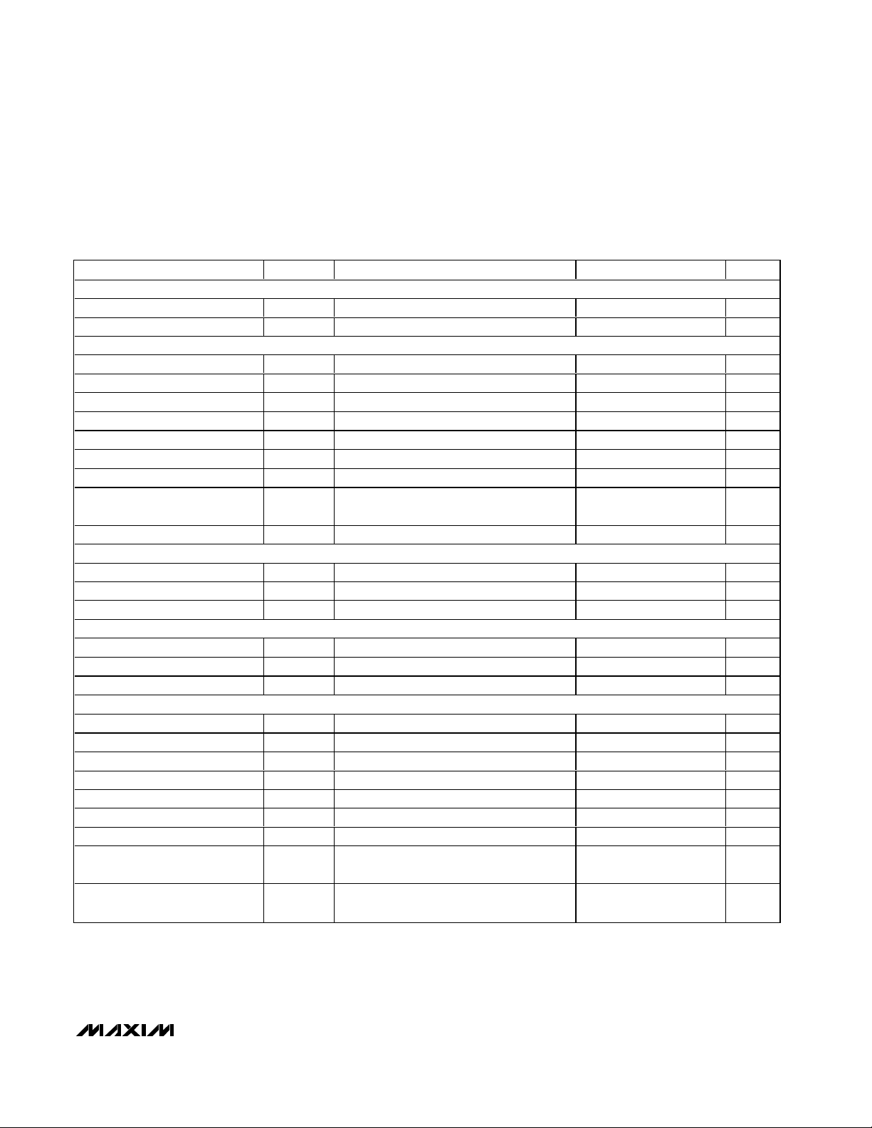
PARAMETER SYMBOL CONDITIONS MIN TYP MAX UNITS
SOFT-START/REFERENCE (CSS)
Reference Voltage V
Soft-Start Pullup Current I
ERROR AMPLIFIER (CSS, FB, COMP)
FB Input Range V
FB Input Current I
COMP Output Range Inferred from FB offset voltage test 2.1 6.0 V
COMP Output Sink Current VFB = 3V 20 mA
COMP Output Source Current VFB = 0V 30 mA
Open-Loop Gain G
Unity-Gain Bandwidth BW C
FB Offset Voltage V
COMP Output Slew Rate SR C
PVIN UNDERVOLTAGE LOCKOUT (STT)
PVIN Undervoltage Lockout V
STT Threshold V
STT Input Impedance R
INTEGRATING FAULT PROTECTION (FLTINT)
FLTINT Source Current I
FLTINT Shutdown Threshold V
FLTINT Restart Hysteresis V
OSCILLATOR (RCOSC, SYNCIN, SYNCOUT)
PWM Period t
Maximum PWM Duty Cycle D
Maximum RCOSC Frequency f
Maximum SYNCIN Frequency f
SYNCIN High-Level Voltage VH
SYNCIN Low-Level Voltage VL
SYNCIN Pulldown Resistor 100 kΩ
SYNCIN Rising to SYNCOUT
Falling Delay
SYNCIN Falling to SYNCOUT
Rising Delay
CSS
CSS
FB
FB
A
OS
STT
STT
FLTINT
FLTINTSDVFLTINT
FLTINTHY
S
MAX
RCOSCMAX
SYNCIN
SYNCIN
SYNCIN
1.215 1.235 1.255 V
70 µA
Inferred from FB offset voltage test 0 3 V
VFB = V
REF
2.1V < V
COMP
VFB = 0 to 3V; V
I
COMP
COMP
rising 22 23.5 25 V
PVIN
V
rising 1.18 1.24 1.30 V
STT
< 6V 80 dB
COMP
= 50pF, I
= -5mA to +5mA
= ±5mA 3 MHz
COMP
= 2.1V to 6V;
COMP
-3 +3 mV
= 50pF 1 V/µs
±250 nA
100 kΩ
V
= 0V 90 µA
FLTINT
= rising 2.9 V
0.9 V
R
R
RCOSC
RCOSC
= 24kΩ, C
= 24kΩ, C
= 100pF 3.9 µs
RCOSC
= 100pF 48 %
RCOSC
1 MHz
50% duty cycle 500 kHz
Pulse rising 2.1 V
Pulse falling 0.8 V
30 ns
70 ns
Page 4
MAX5051
Parallelable, Clamped Two-Switch
Power-Supply Controller IC
4 _______________________________________________________________________________________
ELECTRICAL CHARACTERISTICS (continued)
(AVIN = 12V, PVIN = 12V, V
UVLO
= V
STT
= 3V, V
CON
= 3V, R
RCOSC
= 24kΩ, C
CSS
= 10nF, C
RCOSC
= 100pF, C
REG9
= 4.7µF,
C
REG5
= 4.7µF, TA= T
MIN
to T
MAX
, unless otherwise noted. Typical values are at TA= +25°C. All driver, voltage-regulator, and refer-
ence outputs unconnected except for bypass capacitors.)
)
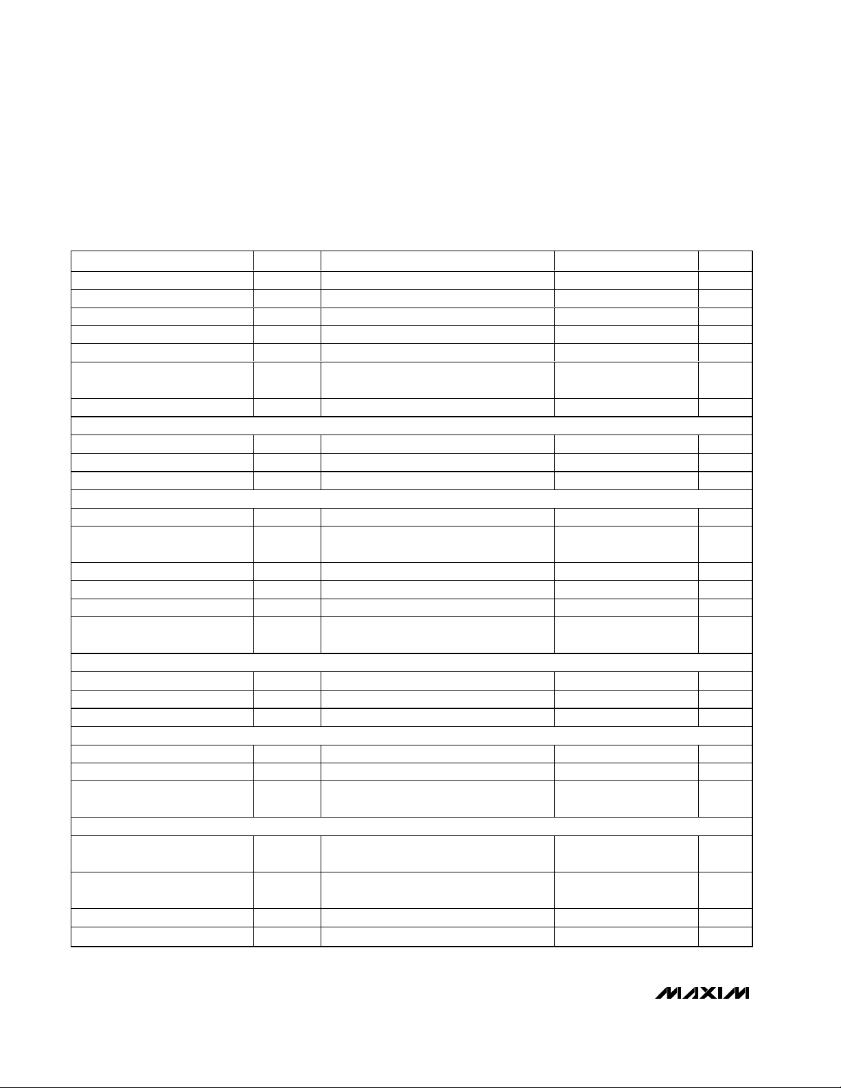
PARAMETER SYMBOL CONDITIONS MIN TYP MAX UNITS
SYNCOUT Voltage High Sourcing 1.2mA 4.5 5.1 V
SYNCOUT Voltage Low Sinking 2.4mA 0.3 V
RCOSC Peak Trip Level V
RCOSC Valley Trip Level 0.2 V
RCOSC Input Bias Current -0.3 µA
RCOSC Discharge MOSFET
R
DS(ON)
RCOSC Discharge Pulse Width 50 ns
UNDERVOLTAGE LOCKOUT (UVLO)
UVLO Threshold V
UVLO Hysteresis V
UVLO Input Bias Current I
PWM COMPARATOR
RCFF Input Voltage Range 0 3 V
Feed-Forward Discharge
MOSFET R
DS(ON)
CON Input Voltage Range 06V
RCFF Level-Shift Voltage V
CON Input Bias Current I
Propagation Delay to Output t
SYNCHRONOUS RECTIFIER PULSE TRANSFORMER DRIVER (LXVDD, LXH, LXL)
High-Side MOSFET R
Low-Side MOSFET R
DS(ON)
DS(ON)
LXH Rising to DRVL Rising Delay 90 ns
CURRENT-LIMIT COMPARATOR (CS)
Current-Limit Threshold Voltage V
Current-Limit Input Bias Current I
Propagation Delay to Output t
LOW-SIDE MOSFET DRIVER (DRVDD, DRVL, PGND)
Peak Source Current
Peak Sink Current
DRVL Resistance Sourcing I
DRVL Resistance Sinking I
TH
2.5 V
Sinking 10mA 50 100 Ω
V
UVLO
HYS
BUVLOVUVLO
R
DS(RCFF
CPWM
CON
dCPWM
R
DSLXH
R
DSLXL
ILIM
BILIM
dILIM
rising 1.18 1.24 1.30 V
UVLO
130 mV
= 2.5V -100 +100 nA
Sinking 10mA 50 100 Ω
2.2 2.4 V
-2 +2 µA
DRVH, DRVL = unconnected, overdrive =
50mV, measured from CON to DRVL
LXH sourcing 10mA, V
LXL sinking 10mA, V
LXVDD
LXVDD
= V
= V
REG5
REG5
3 6.5 12 Ω
2.0 5 10 Ω
90 ns
144 154 164 mV
0 < VCS < 0.3V -2 +2 µA
DRVH, DRVL = unconnected, overdrive =
10mV, measured from CS to DRVL
V
= 0V, pulse width < 100ns;
DRVL
V
= V
DRVDD
V
DRVL
V
DRVDD
DRVL
DRVL
REG9
= V
REG9
= V
REG9
= 50mA, V
= -50mA, V
, pulse width < 100ns;
= V
DRVDD
DRVDD
= V
REG9
REG9
100 ns
2A
5A
1.7 3.5 Ω
0.6 1.4 Ω
Page 5
MAX5051
Parallelable, Clamped Two-Switch
Power-Supply Controller IC
_______________________________________________________________________________________ 5
ELECTRICAL CHARACTERISTICS (continued)
(AVIN = 12V, PVIN = 12V, V
UVLO
= V
STT
= 3V, V
CON
= 3V, R
RCOSC
= 24kΩ, C
CSS
= 10nF, C
RCOSC
= 100pF, C
REG9
= 4.7µF,
C
REG5
= 4.7µF, TA= T
MIN
to T
MAX
, unless otherwise noted. Typical values are at TA= +25°C. All driver, voltage-regulator, and refer-
ence outputs unconnected except for bypass capacitors.)
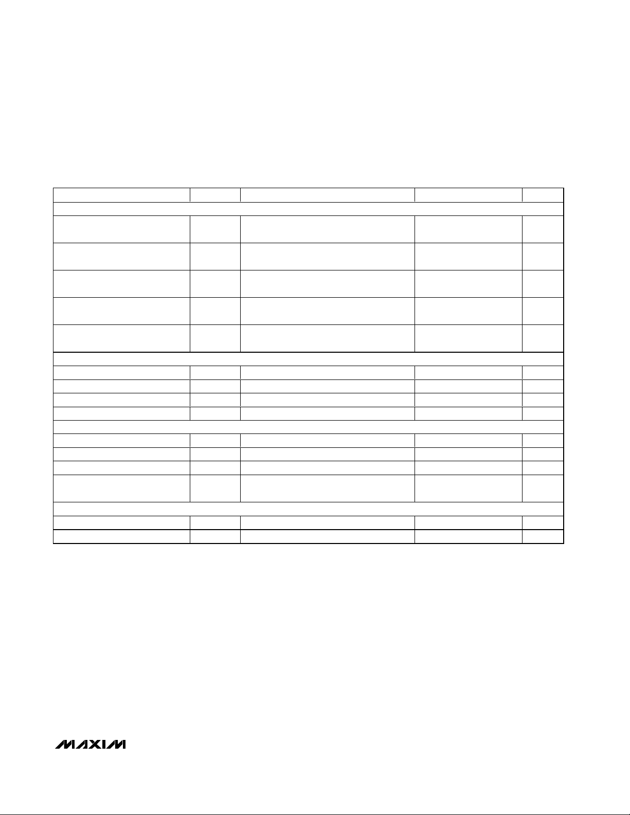
HIGH-SIDE MOSFET DRIVER (BST, DRVH, XFRMRH)
Peak Source Current
Peak Sink Current
DRVH Resistance Sourcing
DRVH Resistance Sinking
Skew Between Low-Side and
High-Side Drivers
BOOST CAPACITOR CHARGE MOSFET (DRVB)
DRVB Resistance Sourcing I
DRVB Resistance Sinking I
Delay from Clock Fall 200 ns
One-Shot Pulse Width 300 ns
STARTUP (STARTUP)
Startup Threshold V
Startup Threshold Hysteresis 330 mV
Internal Pullup Current I
S TARTU P P ul l d ow n M OS FE T
R
D S ( ON )
OVERTEMPERATURE SHUTDOWN
Shutdown Junction Temperature Temperature rising 150 °C
Hysteresis 10 °C
PARAMETER SYMBOL CONDITIONS MIN TYP MAX UNITS
STARTUPVSTARTUP
STARTUP
V
= GN D , p ul se w i d th < 100ns,
D RV H
= V
V
B S T
V
D RV H
= V
V
B S T
I
DRVH
V
XFRMRH
I
DRVH
V
XFRMRH
DRVB
DRVB
Sinking 10mA 50 100 Ω
, V
R E G9
= V
, p ul se w i d th < 100ns,
B S T
, V
R E G9
= 50mA, V
= 0V
= -50mA, V
= 0V
= 50mA 8 35 Ω
= 50mA 5 35 Ω
rising 1.4 2.1 V
X FR M R H
X FR M R H
BST
BST
= 0V
= 0V
= V
REG9
= V
REG9
,
,
2A
5A
1.7 3.5 Ω
0.6 1.4 Ω
0ns
50 µA
Page 6
MAX5051
Parallelable, Clamped Two-Switch
Power-Supply Controller IC
6 _______________________________________________________________________________________
Typical Operating Characteristics
(V
AVIN
= V
PVIN
= 12V, V
UVLO
= V
STT
= 3V, V
CON
= 3V, R
RCOSC
= 24kΩ, C
CSS
= 10nF, C
RCOSC
= 100pF, C
REG9
= 4.7µF, C
REG5
=
4.7µF, T
A
= +25°C, unless otherwise noted.)
AVIN STANDBY CURRENT
vs. AVIN SUPPLY VOLTAGE
MAX5051 toc01
AVIN SUPPLY VOLTAGE (V)
AVIN STANDBY CURRENT (µA)
706040 503020
210
220
230
240
250
260
270
280
290
300
200
10 80
V
UVLO
= 0V
AVIN STANDBY CURRENT
vs. TEMPERATURE
MAX5051 toc02
TEMPERATURE (°C)
AVIN STANDBY CURRENT (µA)
1007525 500-25
210
220
230
240
250
260
270
280
200
190
180
-50 125
V
UVLO
= 0V
PVIN STANDBY CURRENT
vs. SUPPLY VOLTAGE
MAX5051 toc03
PVIN SUPPLY VOLTAGE (V)
PVIN STANDBY CURRENT (µA)
706050403020
100
200
300
400
500
600
0
10 80
V
UVLO
= 0V
PVIN STANDBY CURRENT
vs. TEMPERATURE
MAX5051 toc04
TEMPERATURE (°C)
PVIN STANDBY CURRENT (µA)
1007550250-25
100
200
300
400
500
600
0
-50 125
V
UVLO
= 0V
PVIN STARTUP VOLTAGE
vs. TEMPERATURE
MAX5051 toc05
TEMPERATURE (°C)
PVIN STARTUP VOLTAGE (V)
1007550250-25
23.1
23.2
23.3
23.4
23.5
23.6
23.0
-50 125
STT = FLOATING
REG9 OUTPUT VOLTAGE
vs. PVIN VOLTAGE
MAX5051 toc06
PVIN VOLTAGE (V)
REG9 OUTPUT VOLTAGE (V)
706050403020
8.793
8.796
8.799
8.802
8.805
8.970
10 80
REG9 OUTPUT VOLTAGE
vs. TEMPERATURE
MAX5051 toc07
TEMPERATURE (°C)
REG9 OUTPUT VOLTAGE (V)
1007525 500-25
8.72
8.74
8.76
8.78
8.80
8.82
8.84
8.86
8.88
8.90
8.70
-50 125
REG9 OUTPUT VOLTAGE
vs. REG9 OUTPUT CURRENT
MAX5051 toc08
REG9 OUTPUT CURRENT (mA)
REG9 OUTPUT VOLTAGE (V)
14012080 10040 6020
8.1
8.2
8.3
8.4
8.5
8.6
8.7
8.8
8.9
9.0
8.0
0 160
REG5 OUTPUT VOLTAGE
vs. REG5 OUTPUT CURRENT
MAX5051 toc09
REG5 OUTPUT CURRENT (mA)
REG5 OUTPUT VOLTAGE (V)
8070605040302010
4.4
4.8
5.2
5.6
6.0
4.0
090
Page 7
MAX5051
Parallelable, Clamped Two-Switch
Power-Supply Controller IC
_______________________________________________________________________________________ 7
Typical Operating Characteristics (continued)
(V
AVIN
= V
PVIN
= 12V, V
UVLO
= V
STT
= 3V, V
CON
= 3V, R
RCOSC
= 24kΩ, C
CSS
= 10nF, C
RCOSC
= 100pF, C
REG9
= 4.7µF, C
REG5
=
4.7µF, TA= +25°C, unless otherwise noted.)
REG5 OUTPUT VOLTAGE
vs. TEMPERATURE
5.001
5.000
4.999
4.998
4.997
4.996
4.995
4.994
OUTPUT VOLTAGE (V)
4.993
4.992
4.991
4.990
-50 125
TEMPERATURE (°C)
MAX5051 toc10
1007525 500-25
SOFT-START/REFERENCE VOLTAGE
vs. TEMPERATURE
1.245
1.240
1.235
1.230
1.225
1.220
1.215
1.210
SOFT-START/REFERENCE VOLTAGE (V)
1.205
1.200
-50 125
TEMPERATURE (°C)
MAX5051 toc13
1007525 500-25
700
V
UVLO
600
500
400
300
200
AVIN SUPPLY CURRENT (µA)
100
0
-50 125
90
85
80
75
70
CSS SOFT-START CURRENT (µA)
65
60
-50 125
AVIN SUPPLY CURRENT
vs. TEMPERATURE
= 0V
TEMPERATURE (°C)
CSS SOFT-START CURRENT
vs. TEMPERATURE
TEMPERATURE (°C)
MAX5051 toc11
1007550250-25
MAX5051 toc14
1007550250-25
PVIN SUPPLY CURRENT
vs. TEMPERATURE
7.2
V
= 12V
PVIN
7.1
7.0
6.9
6.8
PVIN SUPPLY CURRENT (mA)
6.7
6.6
-50 125
TEMPERATURE (°C)
UVLO THRESHOLD vs. TEMPERATURE
1.240
1.235
1.230
1.225
1.220
UVLO (V)
1.215
1.210
1.205
1.200
-50 125
TEMPERATURE (°C)
1007550250-25
10075-25 0 25 50
MAX5051 toc12
MAX5051 toc15
STT STARTUP THRESHOLD
vs. TEMPERATURE
1.240
1.235
1.230
1.225
1.220
STT (V)
1.215
1.210
1.205
1.200
-50 125
TEMPERATURE (°C)
RCFF LEVEL-SHIFT VOLTAGE
FLTINT CURRENT vs. TEMPERATURE
95
MAX5051 toc16
10075-25 0 25 50
94
93
92
91
90
89
FLTINT CURRENT (µA)
88
87
86
85
-50 125
TEMPERATURE (°C)
1007525 500-25
2.30
2.29
MAX5051 toc17
2.28
2.27
2.26
2.25
2.24
2.23
RCFF LEVEL-SHIFT VOLTAGE (V)
2.22
2.21
2.20
-50 125
vs. TEMPERATURE
MAX5051 toc18
1007525 500-25
TEMPERATURE (°C)
Page 8

MAX5051
Parallelable, Clamped Two-Switch
Power-Supply Controller IC
8 _______________________________________________________________________________________
Typical Operating Characteristics (continued)
(V
AVIN
= V
PVIN
= 12V, V
UVLO
= V
STT
= 3V, V
CON
= 3V, R
RCOSC
= 24kΩ, C
CSS
= 10nF, C
RCOSC
= 100pF, C
REG9
= 4.7µF, C
REG5
=
4.7µF, T
A
= +25°C, unless otherwise noted.)
170
165
160
155
150
CS THRESHOLD VOLTAGE (mV)
145
140
-50 125
CURRENT-LIMIT THRESHOLD
vs. TEMPERATURE
1007550250-25
TEMPERATURE (°C)
OPEN-LOOP GAIN/PHASE
vs. FREQUENCY
100 270
80
MAX5051 toc19
60
40
GAIN (dB)
20
PHASE
0
-20
0.01 10 100 10000.1 1 10,000
GAIN
FREQUENCY (kHz)
MAX5051 toc20
240
210
180
150
120
90
60
30
0
8
7
6
5
4
3
PHASE (DEGREES)
2
COMP OUTPUT VOLTAGE (V)
1
0
-50 125
COMP OUTPUT VOLTAGE
vs. TEMPERATURE
I
= 5mA
SOURCE
I
= 5mA
SINK
TEMPERATURE (°C)
10075-25 0 25 50
MAX5051 toc21
DRVH AND DRVL R
vs. TEMPERATURE
4.0
3.5
3.0
DRVH AND DRVL SOURCING 50mA
2.5
(Ω)
2.0
DSON
R
1.5
1.0
0.5
DRVH AND DRVL SINKING 50mA
0
-50 125
TEMPERATURE (°C)
NORMALIZED SWITCHING FREQUENCY
vs. TEMPERATURE
1.020
1.010
1.000
0.990
0.980
0.970
0.960
NORMALIZED SWITCHING FREQUENCY
SWITCHING
0.950
-50 125
TEMPERATURE (°C)
DSON
LXL AND LXH R
vs. TEMPERATURE
12
11
MAX5051 toc22
10
9
(Ω)
8
DSON
R
7
6
5
4
10075-25 0 25 50
-40 110
LXH SOURCING 10mA
TEMPERATURE (°C)
SYNCIN TO SYNCOUT PROPAGATION
DELAY vs. TEMPERATURE
130
SYNCIN FALL TO SYNCOUT RISE
120
MAX5051 toc25
110
100
90
80
70
60
PROPAGATION DELAY (ns)
50
SYNCIN RISE TO SYNCOUT FALL
40
30
1007550250-25
-50 125
TEMPERATURE (°C)
DSON
LXH SINKING 10mA
8560-15 10 35
1007525 500-25
MAX5051 toc23
MAX5051 toc26
SWITCHING PERIOD vs. R
50
45
40
35
30
25
20
15
SWITCHING PERIOD (µs)
10
5
0
0200
R
RCOSC
RCOSC
MAX5051 toc24
1601208040
(kΩ)
DRVH MAXIMUM DUTY CYCLE
vs. TEMPERATURE
50.0
49.6
49.2
48.8
48.4
48.0
47.6
47.2
DRVH DUTY CYCLE (%)
46.8
46.4
46.0
-50 125
TEMPERATURE (°C)
MAX5051 toc27
1007525 500-25
Page 9

MAX5051
Parallelable, Clamped Two-Switch
Power-Supply Controller IC
_______________________________________________________________________________________ 9
Pin Description
CON TO DRVL PROPAGATION DELAY
vs. TEMPERATURE
MAX5051 toc28
TEMPERATURE (°C)
PROPAGATION DELAY (ns)
1007525 500-25
65
70
75
80
85
90
95
100
105
110
60
-50 125
50mV OVERDRIVE
CS CURRENT LIMIT TO DRVH
PROPAGATION DELAY vs. TEMPERATURE
MAX5051 toc29
TEMPERATURE (°C)
PROPAGATION DELAY (ns)
1007550250-25
90
100
110
120
130
140
150
80
-50 125
50mV OVERDRIVE
Typical Operating Characteristics (continued)
(V
AVIN
= V
PVIN
= 12V, V
UVLO
= V
STT
= 3V, V
CON
= 3V, R
RCOSC
= 24kΩ, C
CSS
= 10nF, C
RCOSC
= 100pF, C
REG9
= 4.7µF, C
REG5
=
4.7µF, T
A
= +25°C, unless otherwise noted.)
PIN NAME FUNCTION
1 RCOSC
2 SYNCOUT Synchronization Output. Synchronization signal to drive SYNCIN of a second MAX5051, if used.
3 RCFF
4 CON
5 CSS
6 COMP Internal Error Amplifier Output
7FB
8 REG5 5V Linear Regulator Output. Bypass REG5 to GND with a 4.7µF ceramic capacitor.
9 REG9 9V Linear Regulator Output. Bypass REG9 to GND with a 4.7µF ceramic capacitor.
10 PVIN
11 STT
12 LXVDD
Osci l l ator Fr eq uency S et Inp ut. C onnect a r esi stor fr om RC OS C to RE G5 and a cap aci tor fr om RC OS C to GN D
to set the osci l l ator fr eq uency. S w i tchi ng fr eq uency i s 1/2 the fr eq uency of the saw tooth si g nal at RC OS C .
Feed-Forward Input. Connect a resistor from RCFF to AVIN and a capacitor from RCFF to GND. This is
the PWM ramp.
PWM Comparator Noninverting Input. Connect CON to the optocoupler output for isolated applications,
or to COMP for nonisolated applications.
Soft-Start and Reference. Connect a 0.01µF or greater capacitor from CSS to GND. The 1.24V reference
voltage appears across this capacitor.
Feedback Input. Inverting input of the internal error amplifier. The soft-started reference is connected to
the noninverting input of this amplifier.
Regulator Voltage Input. Voltage input to the internal 5V and 9V linear regulators. A high-value resistor
connected from the input supply to PVIN provides the necessary current to charge up the startup
capacitor, and the 400µA standby current required by the MAX5051. After startup, the output of a tertiary
winding is used to provide continued bias to the controller.
Startup Threshold Input. Leave STT floating for a default startup voltage of 24V at PVIN. STT can be
modified by connecting external resistors. For high accuracy, choose external resistors with 50kΩ or less
impedance looking back into the divider.
Supply Input for the Secondary-Side Synchronous Pulse Transformer or Optocoupler Driver. LXVDD is
normally connected to REG5.
Page 10

MAX5051
Parallelable, Clamped Two-Switch
Power-Supply Controller IC
10 ______________________________________________________________________________________
Pin Description (continued)
PIN NAME FUNCTION
13 LXH
14 LXL
15 CS
16 DRVL
17 PGND Power Ground
18 DRVDD
19 DRVB
20 XFRMRH Transformer Input. Transformer primary high-side connection.
21 DRVH Gate-Drive Output for High-Side MOSFET
22 BST
23 AVIN Supply Voltage Input. Connect AVIN directly to the input supply line.
24 GND Analog Signal Ground
25 UVLO
26 STARTUP
27 FLTINT
28 SYNCIN
Synchronous-Pulse Transformer Driver, PMOS Open Drain. LXH is the high-side driver for the secondaryside synchronous-pulse transformer. LXH can also drive a high-speed switching optocoupler. If not
used, connect LXH to LXVDD.
Synchronous-Pulse Transformer Driver, NMOS Open Drain. LXL is the low-side driver for the secondaryside synchronous-pulse transformer. LXL can also drive a high-speed switching optocoupler. If not used,
connect LXL to PGND.
Current-Sense Input. The current-limit threshold is internally set to 156mV relative to PGND. The device
has an internal noise filter. If necessary, connect an additional external RC filter.
Gate-Drive Output for Low-Side MOSFET. DRVL is capable of sourcing and sinking approximately 2A
peak current.
Supply Input for Low-Side MOSFET Driver. Bypass DRVDD locally with good quality 1µF || 0.1µF ceramic
capacitors. DRVDD is normally connected to REG9.
Gate-Drive Output for Boost MOSFET. Connect the gate of a small high-voltage external FET to this pin to
enable charging of the high-side boost capacitor connected between pins 20 and 22. This FET may be
necessary to keep the boost capacitor charged at light loads.
Boost Input. Boost supply connection point for the high-side MOSFET driver. Connect at least a 1µF ||
0.1µF ceramic capacitor from BST to XFRMRH with short and wide PC board traces. If the voltage across
the boost capacitor falls below the high-side undervoltage lockout threshold, the DRVH output stops
switching.
Undervoltage Lockout Input. An external voltage-divider from the input supply sets the startup voltage;
the threshold is 1.24V with 130mV hysteresis. UVLO can also be used as a shutdown input. If unused,
connect UVLO to REG5
Startup Input. STARTUP coordinates simultaneous startup of multiple units from faults, during initial turnon, and UVLO recovery. When paralleling the secondaries of two MAX5051’s, the STARTUP inputs of
each device must be connected together.
Faul t Integ r ati on Inp ut. D ur i ng p er si st ent cur r ent- l i m i t faul ts, a cap aci tor connected to FLTIN T i s char g ed
w i th an i nter nal 90µA cur r ent sour ce. S w i tchi ng i s ter m i nated w hen the vol tag e r eaches 2.9V . An exter nal
r esi stor connected i n p ar al l el d i schar g es the cap aci tor . S w i tchi ng r esum es w hen the vol tag e d r op s to 2V .
Synchronization Input. SYNCIN accepts the synchronization signal from SYNCOUT of another MAX5051
and shifts the switching of the synchronized unit by 180° allowing the reduction of input bypass
capacitors. The MAX5051 switches at the same frequency at SYNCIN. SYNCIN must be 50% duty cycle.
Leave SYNCIN floating if unused.
Page 11

MAX5051
Parallelable, Clamped Two-Switch
Power-Supply Controller IC
______________________________________________________________________________________ 11
Functional Diagram
PVIN
STT
UVLO
AVIN
RCOSC
18R
R
9V
LDO
1.25V
1.125V
1.25V
1.125V
INTERNAL
REGULATOR
OSC
REG9 OK
INTERNAL
SUPPLY
1.25V
REFERENCE
OVER
TEMP
5V
LDO
REG5 OK
THERMAL
SHUTDOWN
25µs
RISING-
EDGE
DELAY
SHDN
REG9
REG5
MAX5051
BST
60ns
RISING-
EDGE
DELAY
LEVEL
SHIFT
LEVEL
SHIFT
80µA
DRVH
XFRMRH
DRVDD
DRVL
PGND
LXVDD
LXH
LXL
SYNCIN
SYNCOUT
RCFF
CON
COMP
CSS
GND
FLTINT
2.7V/1.8V
CS
156mV
50µA
LEVEL
SHIFT
2.7V/1.8V
300ns
ONE
SHOT
CILIM
2.34V
CPWM
FB
E/A
SHDN
64µA
SSA
1.25V
SHDN
1
S
D
Q
Q
R
200ns
RISING-
EDGE
DELAY
10MHz
STARTUP
DRVDD
DRVB
Page 12

MAX5051
Detailed Description
The MAX5051 controller IC is designed for two-switch
forward converter power-supply topologies. It incorporates an advanced set of protection features that
makes it uniquely suitable when high reliability and
comprehensive fault protection are required, as in
power supplies intended for telecommunication
equipment. The device operates over a wide 11V to
76V supply range. By using the MAX5051 with a
secondary-side synchronous rectifier circuit, a very
efficient low output voltage and high output-current
power supply can be designed.
In a typical application, the AVIN pin is connected
directly to the input supply. The PVIN pin is connected
to the input supply through a bleed resistor. This is
used to charge up a reservoir capacitor. When the
voltage across this capacitor reaches approximately
24V, then primary switching commences. If the tertiary
winding is able to supply bias to the IC, then self
boot-strapping takes place and operation continues
normally. If the voltage across the reservoir capacitor
connected to PVIN falls below 6.2V, then switching
stops and the capacitor starts charging up again until
the voltage across it reaches 24V.
This device incorporates synchronization circuitry,
enabling the direct paralleling of two devices for higher
output power and lower input ripple current. Using a
single pin, the circuitry synchronizes and shifts the
phase of the second device by 180°. To enable simultaneous wakeup and shutdown, a STARTUP pin is provided. Connect all the STARTUP pins of all MAX5051
devices together to facilitate parallel operation in the
primary side. When each power supply generates different output voltages, connecting the STARTUP pins is
not necessary.
Power Topology
The two-switch forward-converter topology offers
outstanding robustness against faults and transformer
saturation while allowing the use of SO-8 power
MOSFETs with a voltage rating equal to only that of the
input supply voltage.
Voltage-mode control with feed-forward compensation
allows the rejection of input supply disturbances within
a single cycle, similar to that of current-mode controlled
topologies. This control method offers some significant
benefits not possible with current-mode control. These
benefits are:
• No minimum duty-cycle requirement because of current-signal blanking;
• Clean modulator ramp and higher amplitude for
increased stability;
• Stable operating current of the optocoupler LED and
phototransistor for maximized control-loop bandwidth (in current-mode applications, the optocoupler
bias point is output-load dependent);
• Predictable loop dynamics simplifying the design of
the control loop.
The two-switch power topology has the added benefit
of recovering practically all magnetizing as well as the
leakage energy stored in the parasitics of the isolation
transformer. The lower clamped voltages on the primary power FETs allow for the use of low R
DS(ON)
devices.
Figure 2 shows the schematic diagram of a 48V input
3.3V/10A output power supply built around the
MAX5051.
MOSFET Drivers
The MAX5051’s integrated high- and low-side MOSFET
drivers source and sink up to 2A of peak currents,
resulting in very low losses even when switching high
gate charge MOSFETs. The high-side gate driver
requires its own bypass capacitor connected between
BST and XFRMRH. Use high-quality ceramic capacitors
close to these two pins for bypass. Under normal operating conditions, the energy stored in the transformer
parasitics swings the XFRMRH pin to ground while the
transformer is resetting. During this time, the charge on
the boost capacitor connected to the BST pin is replenished. However, under certain conditions, such as
when the magnetizing inductance of the transformer is
very high or when using conventional rectification at the
output, the duty cycle with light loads may become very
small. Thus, the energy stored could be insufficient to
swing XFRMRH to ground and replenish the boost
capacitor. Figure 3 shows the equivalent circuit during
the magnetizing inductance reset interval, assuming
synchronous rectification where the output inductor is
not allowed to run discontinuous.
If the magnetizing inductance is kept below the following minimum, then the boost capacitor charge will
not deplete:
where d is the duty cycle, VINis the input voltage, fSis
the switching frequency, and Q
gtotal
is the total gate
charge for the high-side MOSFET. The above formula is
only an approximation; the actual value will depend on
other parasitics as well.
Ld
V
fQg Af
M
IN
s total s
≤+0 294
0 005
2
2
.
(. )
Parallelable, Clamped Two-Switch
Power-Supply Controller IC
12 ______________________________________________________________________________________
Page 13

If the charge stored on the boost capacitor is not adequately replenished then the gate-driver lockout for the
high-side MOSFET is triggered, stopping the high side
from switching. The low side continues switching, eventually recharging the capacitor, at which point the high
side starts switching again. To prevent this behavior,
use the boost capacitor’s cycle-by-cycle charging circuit to prevent unwanted shutdowns of the high side
(Figure 2). Connect the gate of a small high-voltage
FET (with the same voltage rating or higher as the main
FETs) to the DRVB output of the MAX5051. Connect the
drain of this FET to XFRMRH, and connect the source
to the primary ground. DRVB will briefly (300ns) turn
this FET ON every cycle after the main PWM clock terminates. This allows the boost capacitor to be replenished under all conditions, even when switching stops
completely. A suitable FET for this is BSS123 or equivalent (100V, 170mA rated). The boost-capacitor charge
MAX5051
Parallelable, Clamped Two-Switch
Power-Supply Controller IC
______________________________________________________________________________________ 13
Figure 2. Typical Application Circuit
Figure 3. Boost Capacitor Charging Path During Transformer
Reset
V
IN+
R9
15kΩ
C11
R12
1MΩ
C12
220nF
C13
100pF
C14
390pF
R13
100kΩ
R14
24.9kΩ
R15
1MΩ
V
IN-
0.1µF
FLTINT
GND
RCOSC
STARTUP
RCFF
CON
COMP
STT
FB
R11
39.2kΩ
CSS
UVLO
AVIN
PVIN
MAX5051
SYNCOUT
REG5
R10
10Ω
C10
4.7µFC91µF
SYNCIN
LXVDD
D4
MA111CT
C8
4.7µF
REG9
XFRMRH
LXH
BST
DRVDD
DRVH
DRVB
DRVL
PGND
LXL
R8
2.2kΩ
R6
47Ω
BAT46W
USED FOR
BOOST
CAPACITOR
PRECHARGE
D3
C5
N1
SI4486
N2
SI4486
28mΩ
1µF
D1
R4
D2
B2100
B2100
L
: 150µH
M
P: 14T
S: 4T
T: 6 T
T1
T1
fs = 250kHz
L1
220nF
475Ω
U2
PS2913
C2
2µH
R3
3 x 270µF
MAX8515
3.3V
R1
11.5kΩ
R2
2.55kΩ
10A
R
LOAD
C4
C3
150nF
C1
47nF
D5
R5
10Ω
C7
4.7µF
N3
BSS123
CS
R7
360Ω
C6
270nF
I
BST
BST
I
BST
I
GD
V
IN
REG9
DRVH
DRVL
XFMRH
I
LM
L
M
Page 14

MAX5051
diode is a high-voltage, small-signal Schottky type. It
may be helpful to connect a resistor in series with this
diode to minimize noise as well as reduce the peak
charging currents. As in any other switching powersupply circuit, the gate-drive loops must be kept to a
minimum. Plan PC board layout with the critical current
carrying loops of the circuit as a starting point.
Secondary-Side Synchronization
The MAX5051 has additional (LXH and LXL) outputs to
make the driving of secondary-side synchronous rectifiers possible with a signal from the primary. These signals lead in time, the actual gate drive applied to the
main power FETs, and allow the secondary-side synchronous FETs to be commutated in advance of the
power pulse. The synchronizing pulse is generated
approximately 90ns ahead of the main pulse that drives
the two power FETs.
Synchronization is accomplished by connecting a small
pulse transformer between LXH and LXL, along with
some clamp diodes (D1 and D2 in Figure 4). This is a
small integrated two-switch driver configuration that
allows for full recovery of the stored energy in the magnetizing inductance of the pulse transformer, thereby
significantly reducing the running bias current of the
controller. It also allows for correct transfer of DC levels
without requiring series capacitors with large time constants, assuring correct drive levels for the secondary
circuit.
Select a pulse transformer, T1, so the current buildup in
its magnetizing inductance is low enough not to create
a significant voltage droop across the internal driver
FETs. Use the following formula to calculate the
approximate value of the primary magnetizing inductance of T1:
where R
dsLXH
and R
dsLXL
are the internal high- and lowside pulse transformer driver on-resistances, fsis the
switching frequency, LMis the pulse transformer primary
magnetizing inductance, tsis the transition time at the
drains of these FETs (typically < 40ns), and Cdsis the
total drain-source capacitance (approximately 10pF).
Alternatively, a high-speed optocoupler (Figure 5) can
be used instead of the pulse transformer. The lookahead pulse accommodates the propagation delays of
the high-speed optocoupler as well as the delays
through the gate drivers of the secondary-side FETs.
Choose optocouplers with propagation delays of less
than 50ns.
Error Amplifier And Reference Soft-Start
The error amplifier in the MAX5051 has an uncommitted
inverting input (FB) and output (COMP). Use this amplifier when secondary isolation is not required. COMP
can then be directly connected to CON (the input of the
PWM comparator). The noninverting input of the error
amplifier is connected to the soft-start generator and is
also available externally at CSS. A capacitor connected
to CSS is slewed linearly during initial startup with the
70µA internal current source (see Figure 2). This provides a linearly increasing reference to the noninverting
input of the error amplifier forcing the output voltage
also to slew proportionally. This method of soft-start is
superior to other methods because the loop is always
2516.
RR
f
L
t
Cf
dsLXH dsLXL
s
M
s
ds s
+
≤≤
Parallelable, Clamped Two-Switch
Power-Supply Controller IC
14 ______________________________________________________________________________________
Figure 4. Secondary-Side Synchronous Rectifier Driver Using
Pulse Transformer
Figure 5. Secondary-Side Synchronous Rectifier Driver Using
High-Speed Optocoupler
MAX5051
REG5
LXVDD
LXH
LXL
PGND
R1
4.7Ω
D3
1N4148
T1
C1
1µF
D1
D2
T1: PULSE ENGINEERING, PE-68386.
D1, D2: CENTRAL SEMICONDUCTOR, CMOSH-3.
MAX5051
LXVDD
R2
2kΩ
PGND
REG5
LXH
LXL
R1
4.7Ω
R2
2kΩ
C1
1µF
R3
560Ω
U2
PS9715
HIGH-SPEED
OPTO
5V
C2
Page 15

in control. Thus, the output-voltage slew rate is constant
at light or heavy loads. Once the soft-start ends, the
voltage on CSS regulates to 1.24V. Do not load CSS
with external circuitry. A suitable range of capacitors
connected to CSS is from 10nF to 0.1µF. Calculate the
required soft-start capacitor based on the total outputvoltage startup time as follows:
where C
CSS
is the capacitor connected to CSS, tSSis
the soft-start time required for the output voltage to rise
from 0V to the rated output voltage. This only applies
when this amplifier is used for output voltage regulation.
PWM Ramp
The PWM ramp is generated at RCFF. Connect a
capacitor C
RCFF
from RCFF to ground and a resistor
R
RCFF
from RCFF to AVIN. The ramp generated on
RCFF is internally offset by 2.3V and applied to the noninverting input of the PWM comparator. The slope of the
ramp is part of the overall loop gain. The dynamic
range of RCFF is 0 to 3V, and so the ramp peak must
be kept below that. Assuming the maximum duty cycle
approaches 50% at minimum input voltage, use the following formula to calculate the minimum value of either
the ramp capacitor or resistor:
where V
INUVLO
is the minimum input supply voltage
(typically the PWM UVLO turn-on voltage), fS is the
switching frequency, and V
RPP
is the peak-to-peak
ramp voltage, typically 2V.
Allow the ramp peak to be as high as possible to maximize the signal-to-noise ratio. The low-frequency smallsignal gain of the power stage, Gps (the gain from the
inverting input of the PWM comparator to the output)
can be calculated by using the following formula:
where Nspis the secondary-to-primary power transformer turns ratio.
Internal Regulators
The MAX5051 has two internal linear regulators that are
used to power internal and external control circuits. The
9V regulator, REG9, is primarily used to power the high-
and low-side gate drivers. Bypass REG9 with a 4.7µF
ceramic capacitor or any other high-quality capacitor;
use low-value ceramics in parallel as necessary. A 5V
regulator also is provided, REG5, primarily used to bias
the internal circuitry of the MAX5051. Bypass REG5 with
a 4.7µF ceramic capacitor similar to the one used for
REG9. Both of these regulators are always powered.
When using bootstrapped startup through a bleed resistor, do not load these outputs while the MAX5051 is in
standby as it may fail to start. Any external loading to
this output should be such that the sum of their load and
the standby current through PVIN of the MAX5051 is
less than the current that the bleed resistor can supply.
Startup Modes
The MAX5051 can be configured for two different
startup modes, allowing operation in either bootstrapped or direct power mode.
Direct Power Mode
In direct power mode, AVIN and PVIN are connected
directly to the input supply. This is typical in 12V to 24V
systems. The undervoltage lockout set at STT needs to
be adjusted down with an external resistor-divider to an
appropriate level.
Bootstrapped Startup
In bootstrap mode, a resistor is connected from the
input supply to PVIN, where a capacitor to GND is
charged towards the input supply. When this voltage
reaches the startup threshold, the device wakes up and
begins switching. A tertiary winding from the transformer is then used to sustain operation. The MAX5051
draws little current from PVIN before reaching the
threshold, which allows a large-value bootstrap resistor
and reduces its power dissipation after startup. A large
startup hysteresis helps the design of the bootstrap
circuit by providing longer running times during startup.
After coming out of standby and before initiating the
soft-start, the MAX5051 turns on the low-side FET to
charge up the boost capacitor. A voltage detector has
been incorporated in the high-side driver that prevents
the high-side switch from turning on with insufficient
voltage. It is also used to indicate when the boost
capacitor has been charged. Once the capacitor is
charged, soft-start commences. If the duty cycle is low,
the magnetizing energy in the transformer may be
insufficient to keep the bootstrap capacitor charged.
DRVB (see Figure 2 dotted lines) has been provided to
drive a small external FET connected between
XFRMRH and PGND, and is pulsed every cycle to keep
the capacitor charged.
GNR C f
ps sp RCFF RCFF s
=
RC
V
fV
RCFF RCFF
INUVLO
s RPP
≥
2
CFst
CSS SS
=µ ×56 /
MAX5051
Parallelable, Clamped Two-Switch
Power-Supply Controller IC
______________________________________________________________________________________ 15
Page 16

MAX5051
Normally PVIN is derived from a tertiary winding of the
transformer. However, at startup there is no energy
delivered through the transformer, hence, a special
bootstrap sequence is required. Figure 6 shows the
voltages on PVIN, REG9, and REG5 during startup.
Initially, PVIN, REG9, and REG5 are 0V. After the input
voltage is applied, C21 (Figure 8) charges PVIN
through the startup resistor, R22, to an intermediate
voltage. At this point, the internal regulators begin
charging C3 and C4. The MAX5051 uses only 400µA
(typ) of the current supplied by R22, and the remaining
current charges C21, C3, and C4. The charging of C4
and C3 stops when their voltages reach approximately
5V and 9V, respectively, while PVIN continues rising
until it reaches the wakeup level of 24V. Once PVIN
exceeds this wakeup level, switching of the external
MOSFETs begins and energy is transferred to the secondary and tertiary outputs. When the voltage on the
tertiary output builds to higher than 9V, startup has
been accomplished and operation is sustained.
However, if REG9 drops below 6.2V (typ) before startup
is complete, the device goes back into standby. In this
case, increase the value of C21 to store enough energy
allowing for voltage buildup at the tertiary winding.
Startup Time Considerations
The PVIN bypass capacitor, C21, supplies current
immediately after wakeup (see Figure 8). The size of
C21 and the connection of the tertiary winding determine the number of cycles available for startup. Large
values of C21 increase the startup time and supply
gate charge for more cycles during initial startup. If the
value of C21 is too small, REG9 drops below 6.2V
because the MOSFETs did not have enough time to
switch and build up sufficient voltage across the tertiary
output to power the device. The device goes back into
standby and will not attempt to restart until PVIN rises
above 24V. Use a low-leakage capacitor for C21, C3,
and C4 (see Figure 8). Generally, power supplies keep
typical startup times to less than 500ms even in low-line
conditions (36VDC for telecom applications). Size the
startup resistor, R22 (Figure 8) to supply both the maximum startup bias of the device and the charging current for C21, C3, and C4.
Oscillator and Synchronization
The MAX5051 oscillator is externally programmable
through a resistor and capacitor connected to RCOSC.
The PWM frequency will be 1/2 the frequency at RCOSC
with a 50% duty cycle, and is available at SYNCOUT.
The maximum duty cycle is limited to < 50% by a 60ns
internal blanking circuit in the power drivers in addition
to the gate and driver delays.
Use the following formula to calculate the oscillator
components:
where C
PCB
is the stray capacitance on the PC board
(about 14pF), REG5 = 5V, VTHis the RCOSC peak trip
level, and fsis the switching frequency.
The MAX5051 contains circuitry that allows it to be synchronized to an external clock whose duty cycle is 50%.
For proper synchronization, the frequency of this clock
should be 15% to 20% higher than half the RCOSC frequency of the MAX5051’s internal oscillator. This is
because the external source SYNCIN directly drives the
power stage, whereas the internal clock is divided by
two. The synchronization feature in the MAX5051 has
been designed primarily for two devices connected to
the same power source with a short physical distance
between the two circuits. Under these circumstances,
the SYNCOUT from one of the circuits can be connected to the SYNCIN of the other one; this forces the power
cycle of the second unit to be 180° out-of-phase. To
synchronize a second MAX5051, feed the SYNCOUT of
the first device to the SYNCIN of the second device. If
necessary, many devices can be daisy-chained in this
manner. Each device will then have 180° phase difference from the device that drives it.
R
RCOSC
s RCOSC PCB
TH
fC C In
REG
REG V
()
≈
+
−
1
2
5
5
Parallelable, Clamped Two-Switch
Power-Supply Controller IC
16 ______________________________________________________________________________________
Figure 6. PVIN, REG5, and REG9 During Startup in
Bootstrapped Mode
PVIN
10V/div
REG9
5V/div
REG5
5V/div
40ms/div
Page 17

Integrating Fault Protection
The integrating fault protection feature allows transient
overcurrent conditions to be ignored for a programmable
amount of time, giving the power supply time to behave
like a current source to the load. This can
happen, for example, under load-current transients when
the control loop requests maximum current to keep the
output voltage from going out of regulation. The fault
integration time can be programmed externally by connecting a suitably sized capacitor to the FLTINT pin.
Under sustained overcurrent faults, the voltage across
this capacitor is allowed to ramp up towards the FLTINT
shutdown threshold (2.9V, typ). Once the threshold is
reached, the power supply shuts down. A high-value
bleed resistor connected in parallel with the FLTINT
capacitor allows it to discharge towards the restart
threshold (1.8V, typ). Once this threshold is reached, the
supply restarts with a new soft-started cycle.
Note that cycle-by-cycle current limiting is provided at
all times by CS with a threshold of 154mV (typ). The
fault integration circuit works by forcing a 90µA current
out of FLTINT every time that the current-limit comparator (Figure 1, CILIM) is tripped. Use the following formula to calculate the value of the capacitor necessary for
the desired shutdown time of this circuit.
where I
FLTINT
= 90µA, tSHis the desired fault integration time after the first shutdown cycle during which
current-limit events from the current-limit comparator
are ignored. For example, a 0.1µF capacitor gives a
fault integration time of 2.25ms.
Some testing may be required to fine-tune the actual
value of the capacitor. To calculate the required bleed
resistance R
FLTINT
, use the following formula:
where tRTis the desired recovery time.
Typically choose tRT= 10 x tSH. Typical values for t
SH
range from a few hundred microseconds to a few milliseconds.
Synchronizing Primary-Side STARTUP For
Parallel Operation
Figure 7 shows the connection diagram of two or more
MAX5051s for synchronized primary-side operation.
The common connection of STARTUP ensures all paralleled modules wakeup and shutdown in tandem. This
helps prevent startup conflicts when the secondaries of
the power supplies are paralleled. Connecting
SYNCOUT to SYNCIN is not necessary; however, when
used, this minimizes the ripple current though the input
bypass capacitors.
Applications Information
Isolated Telecom Power Supply
Figure 8 shows a complete design of an isolated synchronously rectified power supply with a 36V to 72V
telecom voltage range. This power supply is fully protected and can sustain a continuous short circuit at its
output terminals. Figures 9 though 14 show some of the
performance aspects of this power-supply design. This
circuit is available as a completely built and tested
evaluation kit.
R
t
C
FLTINT
RT
FLTINT
=
×0 372.
C
It
V
FLTINT
FLTINT SH
=
.09
MAX5051
Parallelable, Clamped Two-Switch
Power-Supply Controller IC
______________________________________________________________________________________ 17
Figure 7. Connection for Synchronized STARTUP of Two or
More MAX5051s
#1
RCOSC
SYNCOUT
RCFF
CON
#2
RCOSC
SYNCOUT
RCFF
CON
MAX5051
MAX5051
SYNCIN
FLTINT
STARTUP
UVLO
SYNCIN
FLTINT
STARTUP
UVLO
Page 18

MAX5051
Parallelable, Clamped Two-Switch
Power-Supply Controller IC
18 ______________________________________________________________________________________
Figure 8. Schematic of a 48V Input 3.3V at 15A Output Synchronously Rectified, Isolated Power Supply
DRVB
R28
R26
560Ω
1
AN
U6
VCC
OUT
5
4
0.1µF
5V
6
5
IN-
IN+
U7
V+
P_OUT
1
2
5V
C30
0.1µF
IN
R22
15kΩ
PVIN +V
C21
OUT
V
C27
0.15µF
0Ω
R20
LXL
14
TP3
REG5
LXH
IN
+V
XFRMRH
R4
1MΩ
28
SYNCIN
U1
RCOSC
1
C1
1%
R21
24.9kΩ
REG5
8
N1
2
3
D2
IN
+V
1%
100pF
IN
-V
IN
+V
C25
0.07µF
100V
C12
1µF
100V
C11
0.47µF
100V
C10
0.47µF
100V
6
7
5
4
1
21
R5
R6
1MΩ
C7
0.22µF
27
FLTINT
MAX5051
2
TP1
R25
IN
+V
R29
XFRMRH
3
5V
C35
1%
38.3kΩ
1%
26
STARTUP ON/OFF
RCFF
SYNCOUT
3
100kΩ
1µF
25
C2
1Ω
N5
UVLO
390pF
1
8
IN OUT
1
IN
+V
24
2
C16
3.3µF
7
WDI
U5
EN
2
C32
D6
21
REG9
R7
0Ω
2
D1
23
GND
AVIN
5
VOUT
C33
1µF
OUT
V
C15
270µF
C14
270µF
C13
L1
R13
DRVH
31.6kΩ
10.5kΩ
2.4µH
XFRMRH
47Ω
R8
XFRMRH
20
XFRMRH
1%
1%
270µF
N4
6
5
7
8
1
D4
T1
2
C34
8.2Ω
DRVB
REG9
19
18
DRVB
REG5
C4
4.7µF
6
5
N.C.
HOLD
GND
RESET
3
4
1µF
C8
4.7µF
22
21
BST
CSS4COM6COMP7FB8REG5
R15
C5
4700pF
R16
D8
21
10V
4V
4V
4V
3
2
R10
8
8T
330pF
+VIN
DRVDD
REG9
C3
C9
2
20Ω
D3
SGND
4
1
5
9
4.7µF
4
3
C23
1
8
5
6
12
1µF
17
PGND
REG9
PVIN
C6
GND
U4
N_OUT
1000pF
2T
7
R9
10
0.1µF
N2
8.2Ω
5
IN-
P_OUT
2
5V
4
16CS15
PVIN
6
10
4T
2
DRVL
5
3
1
11
LXH
5V
C31
6
IN+
V+
1
C29
0.1µF
4
N3
1
7
2
3
8
1
2
D7
6
R18
D5
2
STT12LXVDD13LXH
4.7Ω
1
1%
R17
0.027Ω
R14
150Ω
C20
220pF
IC_PADDLE
C19
1µF
C18
100pF
R27
10Ω
REG5
2kΩ
2
CA
GND
3
U1: MAX5051
U2: PS2913-1-M
U3: MAX8515
U4, U7: MAX5048A
U5: MAX5023M
U6: PS9715
N1, N2: SI4486
N3, N4: SI4864
N5: BSS123
4
GND
M_OUT
3
80V
4.7µF
R19
R12
475Ω
100kΩ
1
U2
4
R3
2.2kΩ
C24
C26
0.1µF
REG9
2kV
C22
2200pF
R24
OUT
V
1
4
IN
GND
PGND
U3
OUT
FB
3
52
R2
2.55kΩ
1%
TRIM
R1
1%
1%
R11
2
3
360Ω
1000pF
11.5kΩ
C28
0.047µF
OUT
V
C36
0.22µF
C17
0.33µF
10Ω
SENSE (+) SENSE (-)
R23
10Ω
Page 19

MAX5051
Parallelable, Clamped Two-Switch
Power-Supply Controller IC
______________________________________________________________________________________ 19
Figure 9. Efficiency at Nominal Output Voltage vs. Load
Current 48V Nominal Input Voltage
Figure 10. Power Dissipation at Nominal Output Voltage vs.
Load Current for 48V Input Voltage.
Figure 11. Turn-On Transient at Full Load (Resistive Load)
Figure 12. Output Voltage Response to Step-Change in Load
Current
95
90
85
80
75
EFFICIENCY (%)
70
65
60
0462 8 10 12 14
LOAD CURRENT (A)
RL = 0.22Ω
V
OUT
1V/div
8
7
6
5
4
3
POWER DISSIPATION (W)
2
1
0
0462 8 10 12 14
LOAD CURRENT (A)
V
OUT
100mV/div
I
OUT
5A/div
4ms/div
I
OUT
5A/div
1ms/div
50% > 75% > 50% OF I
OUT(MAX)
, dl/dt = 5A/µs
Page 20

MAX5051
Parallelable, Clamped Two-Switch
Power-Supply Controller IC
20 ______________________________________________________________________________________
Figure 13. Output Voltage Ripple At Nominal Input Voltage and
Full Load Current (Scope Bandwidth = 20MHz)
Figure 14. Load Current (10A/div) as a Function of Time When
the Converter Attempts to Turn On into a 50mΩ Short Circuit
Chip Information
TRANSISTOR COUNT: 2049
PROCESS: BiCMOS/DMOS
Exposed Paddle Connected to GND
28
27
26
25
24
23
22
21
20
19
18
17
16
15
1
2
3
4
5
6
7
8
9
10
11
12
13
14
SYNCIN
FLTINT
STARTUP
UVLO
GND
AVIN
CS
BST
DRVH
XFRMRH
DRVB
DRVDD
PGND
DRVL
LXL
LXH
LXVDD
STT
PVIN
REG9
REG5
FB
COMP
CSS
CON
RCFF
SYNCOUT
RCOSC
TSSOP
TOP VIEW
EXPOSED PADDLE IS INTERNALLY CONNECTED TO GND.
MAX5051
Pin Configuration
A
V
OUT
50mV/div
B
I
OUT
10A/div
I
OUT
10A/div
2µs/div
A: 1ms/div
B: 20ms/div
Page 21

MAX5051
Parallelable, Clamped Two-Switch
Power-Supply Controller IC
Maxim cannot assume responsibility for use of any circuitry other than circuitry entirely embodied in a Maxim product. No circuit patent licenses are
implied. Maxim reserves the right to change the circuitry and specifications without notice at any time.
Maxim Integrated Products, 120 San Gabriel Drive, Sunnyvale, CA 94086 408-737-7600 ____________________ 21
© 2003 Maxim Integrated Products Printed USA is a registered trademark of Maxim Integrated Products.
Package Information
(The package drawing(s) in this data sheet may not reflect the most current specifications. For the latest package outline information,
go to www.maxim-ic.com/packages
.)
TSSOP 4.4mm BODY.EPS
 Loading...