

Page 1

General Description
The MAX4987AE/MAX4987BE are overvoltage protection
devices with built-in ESD protection for USB data lines.
These devices feature a low 100mΩ (typ) RONinternal
nFET switch and protect low-voltage systems against voltage faults up to +28V. When the input voltage exceeds
the overvoltage threshold or decreases below the undervoltage threshold, the internal nFET switch is turned off to
prevent damage to the protected components.
All switches feature a minimum 1.5A current-limit protection. During a short-circuit occurrence, the switch
operates in an autoretry mode where the internal nFET
switch is turned on to check if the fault has been
removed. The autoretry interval is 30ms, and if the fault
is removed, the nFET switch remains on.
The MAX4987AE/MAX4987BE feature low-capacitance
(3pF) ESD protection for USB data lines that allow
transmission of high-speed USB 2.0 signals.
The overvoltage threshold (OVLO) is preset to 6.15V.
The undervoltage thresholds (UVLO) are preset to 2.55V
(MAX4987AE) or 4.2V (MAX4987BE). When the input
voltage drops below the undervoltage (UVLO) threshold, the devices enter a low-current standby mode.
All devices are offered in a small 2mm x 3mm, 8-pin
TDFN package and operate over the -40°C to +85°C
extended temperature range.
Applications
Cell Phones
Media Players
Features
o Input Voltage Protection Up to +28V
o Integrated Low R
ON
(100mΩ) nFET Switch
o Internal Overcurrent Protection 1.5A (min)
o Overcurrent Protection (Autoretry)
o Enable Input
o Internal 30ms Startup Delay
o Low-Capacitance USB High-Speed Data Line ESD
Protection (3pF)
±15kV Human Body Model
±15kV IEC 61000-4-2 Air Gap
±6kV IEC 61000-4-2 Contact
o Thermal-Shutdown Protection
o 2mm x 3mm, 8-Pin TDFN Package
MAX4987AE/MAX4987BE
Overvoltage-Protection Controller
with USB ESD Protection
________________________________________________________________
Maxim Integrated Products
1
Ordering Information/Selector Guide
19-1059; Rev 0; 11/07
For pricing, delivery, and ordering information, please contact Maxim Direct at 1-888-629-4642,
or visit Maxim’s website at www.maxim-ic.com.
Note: All devices are specified over the -40°C to +85°C operating temperature range.
+
Denotes a lead-free package.
*
Future product—contact factory for availability.
**
EP = Exposed paddle.
Typical Operating Circuit appears at end of data sheet.
Pin Configuration
134
865
OUT
V
CC
MAX4987AE/
MAX4987BE
2
7
IN
*CONNECT EXPOSED
PAD TO GND.
GND CD-CD+
TDFN-EP
2mm x 3mm
TOP VIEW
ENACOK
*EP
PART
MAX4987AEETA+ 8 TDFN-EP** AAI T823-1 2.55 6.15 Autoretry
MAX4987BEETA+* 8 TDFN-EP** AAJ T823-1 4.2 6.15 Autoretry
PINPACKAGE
TOP MARK
PACKAGE
CODE
UVLO (V) OVLO (V)
OVERCURRENT
MODE
Page 2

MAX4987AE/MAX4987BE
Overvoltage-Protection Controller
with USB ESD Protection
2 _______________________________________________________________________________________
ABSOLUTE MAXIMUM RATINGS
ELECTRICAL CHARACTERISTICS
(VIN= +2.2V to +28V, TA= -40°C to +85°C, unless otherwise noted. Typical values are at VIN= +5V and TA= +25°C.)
Stresses beyond those listed under “Absolute Maximum Ratings” may cause permanent damage to the device. These are stress ratings only, and functional
operation of the device at these or any other conditions beyond those indicated in the operational sections of the specifications is not implied. Exposure to
absolute maximum rating conditions for extended periods may affect device reliability.
(All voltages referenced to GND.)
IN ............................................................................-0.3V to +30V
OUT.............................................................-0.3V to +(IN + 0.3V)
V
CC
, EN, ACOK, CD+, CD- ......................................-0.3V to +6V
Continuous Power Dissipation (T
A
= +70°C) for multilayer board:
8-Pin TDFN (derate 16.7mW/°C above +70°C) .........1333mW
Package Junction-to-Ambient Thermal Resistance
(
θ
JA
) (Note 1) ................................................................60.0°C/W
Package Junction-to-Case Thermal Resistance
(
θ
JC
) (Note 1) ................................................................10.8°C/W
Operating Temperature Range ...........................-40°C to +85°C
Junction Temperature......................................................+150°C
Storage Temperature Range .............................-65°C to +150°C
Lead Temperature (soldering) .........................................+300°C
Note 1: Package thermal resistances were obtained using the method described in JEDEC specification JESD51-7, using a 4-layer
board. For detailed information on package thermal considerations, go to www.maxim-ic.com/thermal-tutorial
.
PARAMETER SYMBOL CONDITIONS MIN TYP MAX UNIT
ANALOG SWITCH
Input-Voltage Range V
VCC Input Voltage V
Input Supply Current I
UVLO Supply Current I
IN Undervoltage Lockout V
IN Undervoltage Lockout Hysteresis 1%
Overvoltage Trip Level V
IN Overvoltage Lockout Hysteresis 1%
Switch On-Resistance R
Overcurrent Protection Threshold I
Maximum Output Capacitance VIN = 5V, no overcurrent shutdown 1000 µF
CD+ and CD- Leakage Current I
CD+ and CD- Capacitance C
DIGITAL SIGNALS
ACOK Output Low Voltage V
ACOK High-Leakage Current V
EN Input-Voltage High V
EN Input-Voltage Low V
EN Input-Leakage Current I
IN
CC
EN = 0V, V
IN
EN = 5V, VIN > V
UVLOVIN
(VIN falling)
UVLO
(VIN rising)
OVLO
LIM
LKG_CDVCC
LEAK
(VIN rising) 5.55 6.15 6.45
(VIN falling) 5.5
VIN = 5V, I
ON
f = 1MHz, V
CD
I
OL
SINK
ACOK
IH
IL
VEN = 5.5V -1 +1 µA
< V
= 5.5V, V
= 1mA 0.4 V
= 5.5V, flag deasserted 1 µA
2.2 28 V
> V
IN
UVLO
UVLO
UVLO
MAX4987AE 2.3
MAX4987BE 3.8
MAX4987AE 2.35 2.55 2.75
MAX4987BE 3.85 4.2 4.45
= 500mA 100 200 mΩ
OUT
1.5 4.2 A
= 0V, 3.3V -300 +300 nA
CD_
= 0.5
CD_
P-P
1.4 V
60 150
50 100
3pF
5.5 V
µA
40 µA
V
V
0.4 V
Page 3
MAX4987AE/MAX4987BE
Overvoltage-Protection Controller
with USB ESD Protection
_______________________________________________________________________________________ 3
Note 2: All timing is specified using 20% and 80% levels, unless otherwise noted.
ELECTRICAL CHARACTERISTICS (continued)
(VIN= +2.2V to +28V, TA= -40°C to +85°C, unless otherwise noted. Typical values are at VIN= +5V and TA= +25°C.)
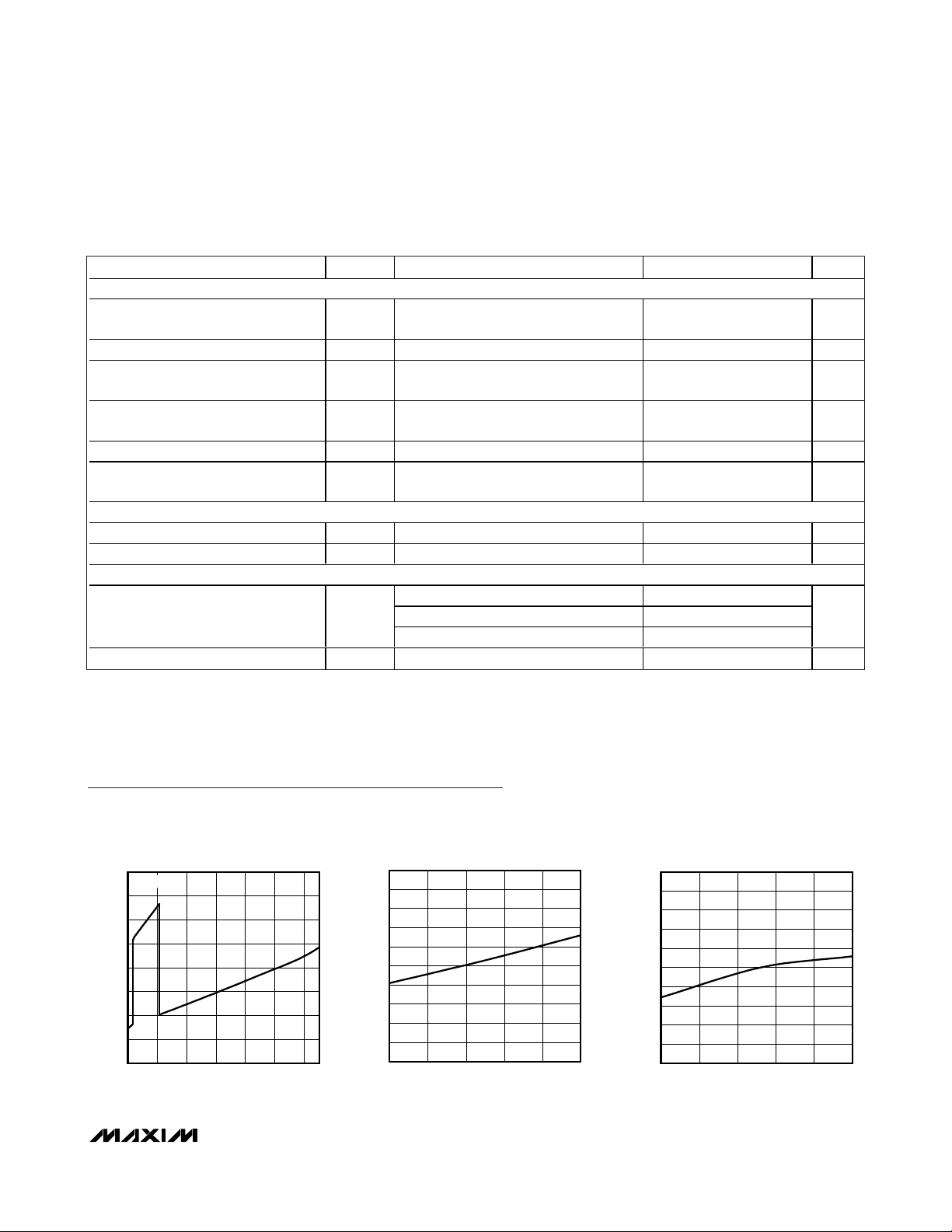
Typical Operating Characteristics
(TA = +25°C, unless otherwise noted.)
TIMING CHARACTERISTICS (Note 2)
Debounce Time t
ACOK Assertion Time t
Switch Turn-On Time t
Switch Turn-Off Time t
Current-Limit Turn-Off Time t
Autoretry Time t
THERMAL PROTECTION
Thermal Shutdown T
Thermal-Shutdown Hysteresis 40 °C
ESD PROTECTION
All Other Pins Human Body Model ±2 kV
PARAMETER SYMBOL CONDITIONS MIN TYP MAX UNIT
INDBC
ACOKVUVLO
ON
OFF
BLANK
RETRY
SHDN
Time from V
charge-pump enable
V
UVLO
from 10% to 90% of V
VIN < V
switch off, R
Overcurrent fault to internal switch off 10 µs
From overcurrent fault to internal switch
turn-on
< VIN < V
< VIN < V
UVLO
< VIN < V
UVLO
OVLO
OVLO
or VIN > V
= 100Ω
LOAD
to
OVLO
30 ms
, to ACOK low 30 ms
, R
= 100Ω,
OUT
OVLO
LOAD
to internal
3ms
10 µs
30 ms
150 °C
Human Body Model ±15
IEC 61000-4-2 Air Gap ±15CD+ and CD-
IEC 61000-4-2 Contact ±6
kV
SWITCH ON-RESISTANCE
vs. TEMPERATURE
0
-40 10-15 35 60 85
TEMPERATURE (°C)
IN SUPPLY CURRENT (μA)
80
70
60
50
40
30
20
10
0
MAX4987AE
210146
IN SUPPLY CURRENT
vs. IN VOLTAGE
18
IN VOLTAGE (V)
22 26
MAX4987AE/BE toc01
(mΩ)
ON
R
200
180
160
140
120
100
80
60
40
20
NORMALIZED UVLO THRESHOLD
1.010
1.008
1.006
MAX4987AE/BE toc02
1.004
1.002
1.000
0.998
0.996
0.994
NORMALIZED UVLO THRESHOLD (V)
0.992
0.990
-40 10-15 356085
vs. TEMPERATURE
MAX4987AE/BE toc03
TEMPERATURE (°C)
Page 4

MAX4987AE/MAX4987BE
Overvoltage-Protection Controller
with USB ESD Protection
4 _______________________________________________________________________________________
Typical Operating Characteristics (continued)
(TA = +25°C, unless otherwise noted.)
0.990
0.996
0.994
0.992
0.998
1.000
1.002
1.004
1.006
1.008
1.010
-40 10-15 356085
NORMALIZED OVLO THRESHOLD
vs. TEMPERATURE
MAX4987AE/BE toc04
TEMPERATURE (°C)
NORMALIZED OVLO THRESHOLD (V)
0.80
0.92
0.88
0.84
0.96
1.00
1.04
1.08
1.12
1.16
1.20
-40 10-15 356085
NORMALIZED CURRENT LIMIT
vs. TEMPERATURE
MAX4987AE/BE toc05
TEMPERATURE (°C)
CURRENT LIMIT (%)
0
2.0
1.0
3.0
4.0
5.0
-40 85
TURN-ON TIME
vs. TEMPERATURE
MAX4987AE/BE toc06
TEMPERATURE (°C)
TURN ON TIME (ms)
10-15 35 60
20.0
30.0
25.0
40.0
35.0
45.0
50.0
-40 85
DEBOUNCE TIME
vs. TEMPERATURE
MAX4987AE/BE toc07
TEMPERATURE (°C)
DEBOUNCE TIME (ms)
10-15 35 60
UNDERVOLTAGE FAULT RESPONSE
MAX4987AE/BE toc10
4μs/div
V
IN
2V/div
5
2
0
0
0
V
OUT
2V/div
I
OUT
1A/div
V
ACOK
5V/div
POWER-UP RESPONSE
MAX4987AE/BE toc08
10ms/div
V
IN
5V/div
V
OUT
5V/div
I
OUT
1A/div
V
ACOK
5V/div
OVERVOLTAGE FAULT RESPONSE
MAX4987AE/BE toc09
2μs/div
V
IN
5V/div
8V
5V
8V
5V
0
0
0
V
OUT
5V/div
I
OUT
1A/div
V
ACOK
5V/div
SHORT-CIRCUIT FAULT RESPONSE
MAX4987AE/BE toc11
10μs/div
V
IN
5V/div
0
0
0
0
V
OUT
5V/div
I
OUT
1A/div
V
ACOK
5V/div
CIN = 100μF
Page 5

MAX4987AE/MAX4987BE
Overvoltage-Protection Controller
with USB ESD Protection
_______________________________________________________________________________________ 5
Pin Description
Functional Diagram
PIN NAME FUNCTION
1IN
Voltage Input. Bypass IN with a 1µF ceramic capacitor as close to the device as possible to obtain
±15kV HBM ESD protection. No capacitor required to obtain ±2kV HBM ESD protection.
2 CD+ USB Data Line
3 GND Ground
4 CD- USB Data Line
5VCCPositive Supply-Voltage Input. VCC is required only when USB signals are present.
6 EN Enable Active-Low Input. Drive EN low to enable the switch. Drive EN high to disable the switch.
voltage is stable
IN
7 ACOK
Open-Drain Adapter-Voltage Indicator Output. ACOK is driven low after the V
between UVLO and OVLO for 30ms (typ). Connect a pullup resistor from ACOK to the logic I/O voltage
of the host system.
8 OUT Output Voltage. Output of internal switch.
EP EP Exposed Pad. Connect exposed pad to ground. Do not use EP as a sole ground connection.
IN
OVERCURRENT
FAULT
CHARGE
PUMP
OUT
ACOK
EN
CONTROL
LOGIC
MAX4987AE/
MAX4987BE
EN
V
CC
CD+
CD-
V
BG
REFERENCE
+
OV
-
+
UV
-
GND
Page 6
MAX4987AE/MAX4987BE
Detailed Description
The MAX4987AE/MAX4987BE are overvoltage protection devices with integrated ESD protection for USB
data lines. These devices feature a low RONinternal
FET and protect low-voltage systems against voltage
faults up to +28V. If the input voltage exceeds the overvoltage threshold, the internal nFET switch is turned off
to prevent damage to the protected components. The
30ms debounce time prevents false turn-on of the internal nFET switch during startup. An open-drain activelow logic output is available to signal that a successful
power-up has occurred.
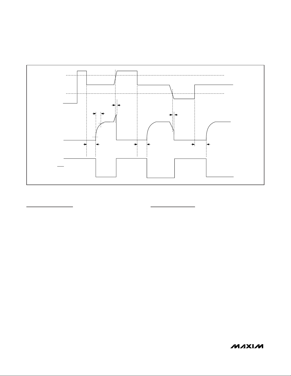
Device Operation
The MAX4987AE/MAX4987BE have an internal oscillator and charge pump that control the turn-on of the
internal nFET switch. The internal oscillator controls the
timers that enable the turn-on of the charge pump and
controls the state of the open-drain ACOK output. If V
IN
< V
UVLO
or if VIN> V
OVLO
, the internal oscillator
remains off, thus disabling the charge pump. If V
UVLO
<
VIN< V
OVLO
, the internal charge pump is enabled. The
charge-pump startup, after a 30ms internal delay, turns
on the internal nFET switch and asserts ACOK (see
Figure 1). At any time, if VINdrops below V
UVLO
or rises
above V
OVLO
, ACOK is pulled high and the charge
pump is disabled.
Internal nFET Switch
The MAX4987AE/MAX4987BE incorporate an internal
nFET switch with a 100mΩ (typ) on-resistance. The
nFET switch is internally driven by a charge pump that
generates a voltage above the input voltage. The
MAX4987AE/MAX4987BE is equipped with a 1.5A (min)
current-limit protection that turns off the nFET switch
within 5µs (typ) during an overcurrent fault condition.
Autoretry
The MAX4987AE/MAX4987BE have an overcurrent
autoretry function that turns on the nFET switch again
after a 30ms (typ) retry time (see Figure 2). If the faulty
load condition is still present after the blanking time, the
switch turns off again and the cycle is repeated. The fast
turn-off time and 30ms retry time result in a very low duty
cycle in order to keep power consumption low. If the
faulty load condition is not present, the switch remains on.
Undervoltage Lockout (UVLO)
The MAX4987AE has a 2.55V undervoltage-lockout
threshold (UVLO), while the MAX4987BE has a 4.15V
UVLO threshold. When VINis less than V
UVLO
, ACOK is
high impedance.
Overvoltage-Protection Controller
with USB ESD Protection
6 _______________________________________________________________________________________
Figure 1. MAX4987AE/MAX4987BE Timing Diagram
t
OUT
OUT
OFF
t
OFF
t
INDBC
IN
OUT
ACOK
t
INDBC
t
ON
90% V
10% V
OVLO
UVLO
t
INDBC
Page 7

Overvoltage Lockout (OVLO)
The MAX4987AE/MAX4987BE have a 6.15V (typ) overvoltage threshold (OVLO). When VINis greater than
V
OVLO
, ACOK is high impedance.
ACOK
ACOK is an active-low open-drain output that asserts
low when V
UVLO
< VIN< V
OVLO
following the 30ms
(typ) debounce period. Connect a pullup resistor from
ACOK to the logic I/O voltage of the host system.
During a short-circuit fault, ACOK may deassert due to
VINnot being in the valid operating voltage range.
Thermal-Shutdown Protection
The MAX4987AE/MAX4987BE feature thermal-shutdown
circuitry. The internal nFET switch turns off when the
junction temperature exceeds T
SHDN
and immediately
goes into a fault mode. The device exits thermal shutdown after the junction temperature cools by +40°C (typ).
Applications Information
IN Bypass Capacitor
For most applications, bypass IN to GND with a 1µF
ceramic capacitor as close to the device as possible to
enable ±15kV HBM ESD protection on IN. If ±15kV HBM
ESD protection is not required, there is no capacitor
required at IN. If the power source has significant inductance due to long lead length, take care to prevent overshoots due to the LC tank circuit and provide protection if
necessary to prevent exceeding the absolute maximum
rating on IN.
ESD Test Conditions
ESD performance depends on a number of conditions.
The MAX4987AE/MAX4987BE are specified for ±15kV
HBM ESD protection on the CD+, CD-, and IN pins
when IN is bypassed to ground with a 1µF ceramic
capacitor. The CD+ and CD- inputs are also protected
against ±15kV Air Gap and ±6kV contact IEC 61000-42 ESD events.
Human Body Model
Figure 3 shows the Human Body Model, and Figure 4
shows the current waveform it generates when discharged into a low impedance. This model consists of
a 100pF capacitor charged to the ESD voltage of interest, that is then discharged into the device through a
1.5kΩ resistor.
IEC 61000-4-2
The IEC 61000-4-2 standard covers ESD testing and performance of finished equipment. It does not specifically
refer to integrated circuits. The MAX4987AE/ MAX4987BE
MAX4987AE/MAX4987BE
Overvoltage-Protection Controller
with USB ESD Protection
_______________________________________________________________________________________ 7
Figure 2. Autoretry Timing Diagram
Figure 3. Human Body ESD Test Model
Figure 4. Human Body Current Waveform
t
OFF
nFET SWITCH
ON
t
CURRENT
THROUGH
nFET SWITCH
RETRY
I
LIM
SWITCH OFF
R
D
1.5kΩ
DISCHARGE
RESISTANCE
STORAGE
CAPACITOR
HIGH-
VOLTAGE
DC
SOURCE
R
C
1MΩ
CHARGE CURRENT-
LIMIT RESISTOR
C
100pF
s
nFET SWITCH
ON
DEVICE
UNDER
TEST
AMPERES
IP 100%
90%
36.8%
10%
0
0
t
RL
I
r
TIME
t
DL
CURRENT WAVEFORM
PEAK-TO-PEAK RINGING
(NOT DRAWN TO SCALE)
Page 8

MAX4987AE/MAX4987BE
are specified for ±15kV Air-Gap Discharge and ±6kV
Contact Discharge IEC 61000-4-2 on the CD+ and CDpins.
The major difference between tests done using the
Human Body Model and IEC 61000-4-2 is a higher peak
current in IEC 61000-4-2, due to lower series resistance.
Hence, the ESD withstand voltage measured to IEC
61000-4-2 generally is lower than that measured using
the Human Body Model. Figure 5 shows the IEC 610004-2 model. The Contact Discharge method connects the
probe to the device before the probe is charged. The
Air-Gap Discharge test involves approaching the device
with a charged probe.
Overvoltage-Protection Controller
with USB ESD Protection
8 _______________________________________________________________________________________
Figure 5. IEC 61000-4-2 ESD Test Model
OVERCURRENT
FAULT
IN
CD+
CD-
OUT
V
CC
CHARGE
PUMP
CONTROL
LOGIC
MAX4987AE/
MAX4987BE
ACOK
V
IO
PHONE
LOAD
V
BG
REFERENCE
+
-
+
-
OV
UV
EN
USB
CONNECTOR
VBUS
D+
D-
USB
TRANSCEIVER
V
CC
D+
D-
GND
V
CC
BATTERY
CHARGER
Typical Operating Circuit
Chip Information
PROCESS: BiCMOS
R
D
330Ω
DISCHARGE
RESISTANCE
STORAGE
CAPACITOR
HIGH-
VOLTAGE
DC
SOURCE
R
C
50MΩ TO 100MΩ
CHARGE-CURRENT-
LIMIT RESISTOR
C
150pF
s
DEVICE
UNDER
TEST
Page 9

MAX4987AE/MAX4987BE
Overvoltage-Protection Controller
with USB ESD Protection
_______________________________________________________________________________________ 9
Package Information
(The package drawing(s) in this data sheet may not reflect the most current specifications. For the latest package outline information,
go to www.maxim-ic.com/packages
.)
8L, TDFN.EPS
PACKAGE OUTLINE
8L TDFN, EXPOSED PAD, 2x3x0.8mm
21-0174
1
B
2
Page 10

MAX4987AE/MAX4987BE
Overvoltage-Protection Controller
with USB ESD Protection
Maxim cannot assume responsibility for use of any circuitry other than circuitry entirely embodied in a Maxim product. No circuit patent licenses are
implied. Maxim reserves the right to change the circuitry and specifications without notice at any time.
10
____________________Maxim Integrated Products, 120 San Gabriel Drive, Sunnyvale, CA 94086 408-737-7600
© 2007 Maxim Integrated Products is a registered trademark of Maxim Integrated Products, Inc.
SPRINGER
Package Information (continued)
(The package drawing(s) in this data sheet may not reflect the most current specifications. For the latest package outline information,
go to www.maxim-ic.com/packages
.)
SYMBOL
A
E
D
A1
L
k 0.20 MIN.
A2
e
b
MIN.
0.70
1.95
0.00
0.30
DIMENSIONS
NOM.
0.75
3.002.95
2.00
0.02
0.40
0.20 REF.
8N
0.50 BSC
0.250.18 0.30
MAX.
0.80
3.05
2.05
0.05
0.50
PKG.
CODE
T823-1
EXPOSED PAD PACKAGE
E2
MIN.
NOM.
1.60
1.75
MAX.
1.90
MIN.
1.50
D2
NOM.
1.63
MAX.
1.75
PACKAGE OUTLINE
8L TDFN, EXPOSED PAD, 2x3x0.8mm
21-0174
2
B
2
 Loading...