

Page 1
General Description
The MAX4978–MAX4981 overvoltage-protection devices
protect low-voltage systems against voltage faults up to
+28V and feature a low 85mΩ RONFET, an active current limiter, and lithium-ion battery overcharge protection (MAX4980/MAX4981). These devices are used to
protect the charger input port on a portable device.
The overvoltage protector feature protects against voltages up to 28V with two different trip thresholds: 5.7V
(MAX4978/MAX4980/MAX4981) and 6.8V (MAX4979).
There is an undervoltage protector with two different trip
thresholds: 4.4V (MAX4978) and 2.63V (MAX4979/
MAX4980/MAX4981).
The overcurrent limiter and battery voltage monitor features provide a second layer of protection for a lithiumion battery charger. The overcurrent limiter is available
in two different thresholds: 0.9A (MAX4978/MAX4979/
MAX4980) and 1.95A (MAX4981). Once current reaches the threshold, it is held for a 20ms blanking time. If
the current is still at the limit after the blanking time, the
FET is turned off, and the device restarts the cycle after
160ms. The battery voltage monitor measures the voltage of a lithium-ion battery and disables the FET if the
battery voltage reaches 4.4V (MAX4980/MAX4981).
The MAX4978–MAX4981 are available in a small 8-pin
TDFN (2mm x 3mm) package and are specified over
the extended -40°C to +85°C temperature range.
Applications
Features
o Input Voltage Protection Up to +28V
o Integrated nFET Switch, 85mΩ (typ)
o Preset Overvoltage Protection Trip Level
5.7V (typ) (MAX4978/MAX4980/MAX4981)
6.8V (typ) (MAX4979)
o Low-Current Undervoltage Lockout Mode
o Overcurrent Protection
o Internal 160ms (typ) Startup Delay
o Thermal-Shutdown Protection
o Battery Overcharge Protection
(MAX4980/MAX4981)
o Startup Debounce Time Indicator
(MAX4978/MAX4979)
o Small, 8-Pin (2mm x 3mm) TDFN Package
MAX4978–MAX4981
Overvoltage Protector with
Active Current Limit
________________________________________________________________
Maxim Integrated Products
1
Ordering Information/Selector Guide
19-4137; Rev 0; 5/08
For pricing, delivery, and ordering information, please contact Maxim Direct at 1-888-629-4642,
or visit Maxim’s website at www.maxim-ic.com.
Note: All devices specified over the -40°C to +85°C operating temperature range.
+
Denotes a lead-free package.
*
EP = Exposed pad.
**
Future product—contact factory for availability.
(mA)
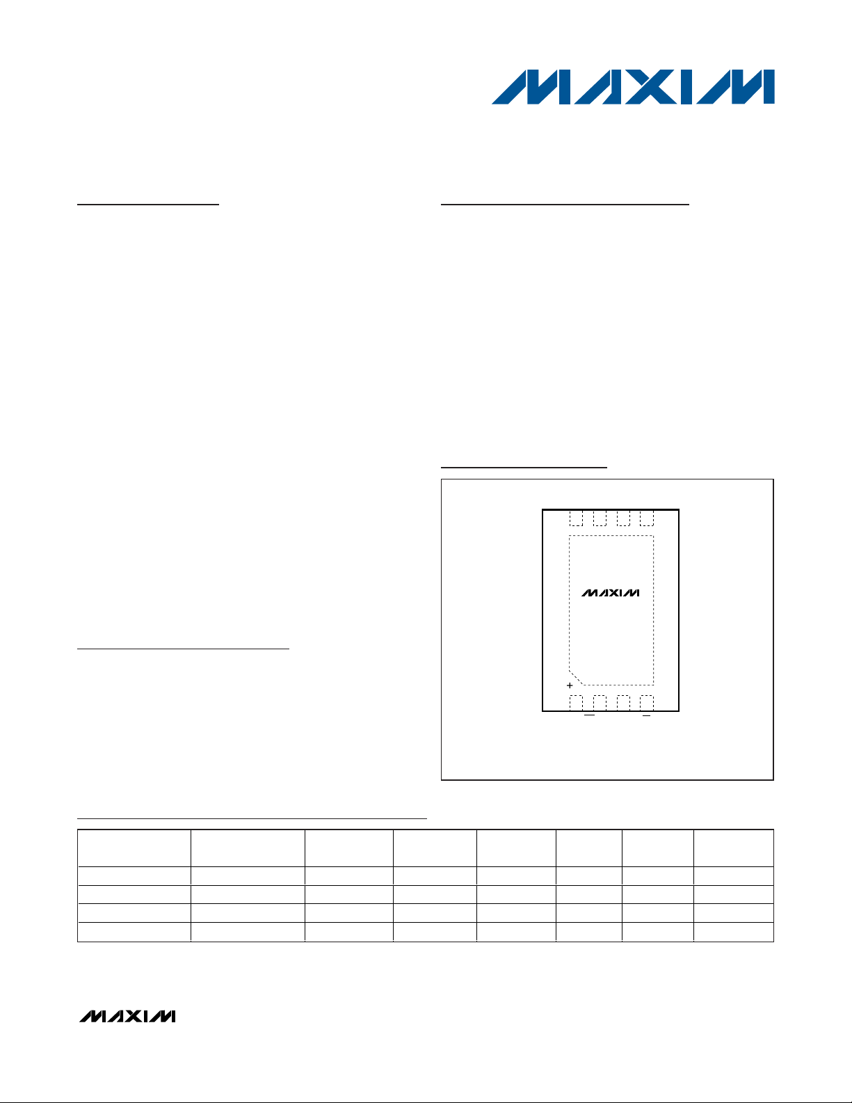
Pin Configuration
134
865
OUT
MAX4978
MAX4979
MAX4980
MAX4981
2
7
IN
(BAT) IS FOR MAX4980/MAX4981 ONLY.
*EP = EXPOSED PAD. CONNECT EP TO GND.
I.C.
TDFN-EP
TOP VIEW
I.C. GNDI.C.
*EP
EN
SDT(BAT)
Typical Application Circuit appears at end of data sheet.
Cell Phones
MP3 Players
Digital Still Cameras
PDAs and Palmtop
Devices
PART PIN-PACKAGE
MAX4978ETA+
MAX4979ETA+**
MAX4980ETA+
MAX4981ETA+
CURRENT
LIMIT
8 TDFN-EP*
8 TDFN-EP*
8 TDFN-EP*
8 TDFN-EP*
900 No 4.4 5.7 AAK T823-1
900 No 2.63 6.8 AAL T823-1
900 Yes 2.63 5.7 AAM T823-1
1950 Yes 2.63 5.7 AAN T823-1
BATTERY
MONITOR
UVLO
(V)
OVLO
(V)
TOP
MARK
PKG
CODE
Page 2
MAX4978–MAX4981
Overvoltage Protector with
Active Current Limit
2 _______________________________________________________________________________________
ABSOLUTE MAXIMUM RATINGS
ELECTRICAL CHARACTERISTICS
(VIN= 5.0V, VEN= 0V, TA= -40°C to +85°C, unless otherwise noted. Typical values are at TA= +25°C.) (Note 2)
Stresses beyond those listed under “Absolute Maximum Ratings” may cause permanent damage to the device. These are stress ratings only, and functional
operation of the device at these or any other conditions beyond those indicated in the operational sections of the specifications is not implied. Exposure to
absolute maximum rating conditions for extended periods may affect device reliability.
(Voltages referenced to GND.)
IN, SDT ................................................................. -0.3V to +30V
OUT ........................................................................... -0.3V to IN
EN, BAT .................................................................. -0.3V to +6V
SDT Continuous Current ................................................. ±50mA
Continuous Power Dissipation (T
A
= +70°C)
8-Pin 2mm x 3mm TDFN (derate 16.7mW/°C
above +70°C) ........................................................... 1333mW
Junction-to-Case Thermal Resistance (
θ
JC
) (Note 1)
8-Pin 2mm x 3mm TDFN ......................................... 10.8°C/W
Junction-to-Ambient Thermal Resistance (
θ
JA
) (Note 1)
8-Pin 2mm x 3mm TDFN ............................................ 60°C/W
Operating Temperature Range ......................... -40°C to +85°C
Junction Temperature .................................................... +150°C
Storage Temperature Range ........................... -65°C to +150°C
Lead Temperature (soldering, 10s) ................................+300°C
Note 1: Package thermal resistances were obtained using the method described in JEDEC specification JESD51-7, using a 4-layer
board. For detailed information on package thermal considerations, refer to www.maxim-ic.com/thermal-tutorial
.
Input Voltage Range V
Input Supply Current I
UVLO Supply Current I
Shutdown Supply Current I
IN Undervoltage Lockout V
IN Undervoltage Lockout
Hysteresis
IN Overvoltage Lockout V
IN Overvoltage Lockout Hysteresis 1%
BAT Overvoltage Trip Level V
BAT Overvoltage Hysteresis MAX4980/MAX4981 1 %
BAT Input Leakage Current I
Switch On-Resistance R
Overcurrent Protection Threshold I
Thermal Shutdown T
PARAMETER SYMBOL CONDITIONS MIN TYP MAX UNITS
IN
I
IN
UVLOVIN
SHDNV EN
UVLO
OVLO
BOTL
LKGB
ONIOUT
LIM
SHDNTA
OUT
MAX4978
MAX4979/MAX4980/
MAX4981
MAX4978/MAX4980/
MAX4981
MAX4979
MAX4980/MAX4981, V
MAX4980/MAX4981, V
MAX4978, MAX4979,
MAX4980
MAX4981
< I
LIM_MIN
= 2.3V 35 60 µA
= 5V 15 23 µA
= 100mA 85 160 mΩ
rising 160 °C
2.3 28 V
VIN falling 4.2
rising 4.3 4.4 4.5
V
IN
VIN falling 2.5
V
rising 2.56 2.63 2.70
IN
VIN falling 5.5
V
rising 5.6 5.7 5.8
IN
VIN falling 6.5
rising 6.65 6.80 6.95
V
IN
rising 4.3 4.4 4.5 V
BAT
= 4.2V 1 µA
BAT
TA=+25°C 850 900 950
TA= 0°C to +85°C 800 1000
T
= -40°C to +0°C 780 1000
A
TA=+25°C 1850 1950 2050
T
= -40°C to +85°C 1750 1950 2150
A
130 190 µA
V
1%
V
mA
Page 3

MAX4978–MAX4981
Overvoltage Protector with
Active Current Limit
_______________________________________________________________________________________ 3
ELECTRICAL CHARACTERISTICS (continued)
(VIN= 5.0V, VEN= 0V, TA= -40°C to +85°C, unless otherwise noted. Typical values are at TA= +25°C.) (Note 2)
Note 2: All devices are 100% production tested at TA= +25°C. Specifications over -40°C to +85°C are guaranteed by design.
Note 3: All timing is measured using 10% and 90% levels, unless otherwise noted.
Thermal-Shutdown Hysteresis 10 °C
EN Input High Voltage V
EN Input Low Voltage V
EN Input Leakage Current I
SDT Output Low Voltage V
SDT Leakage Current I
DYNAMIC (Note 3)
IN Debounce Time t
Switch Turn-On Time t
Switch Turn-Off Time t
Current-Limit Blanking Time t
Current-Limit Reaction Time t
Overcurrent Autoretry Time t
PARAMETER SYMBOL CONDITIONS MIN TYP MAX UNITS
IH
IL
LKGE
OL
LKGS
DEB
ON
OFF
BLANK
REAC
RETRY
V EN = 5.5V or 0V -1 +1 µA
MAX4978/MAX4979, I
MAX4978/MAX4979, V
deasserted
V
< VIN < V
UVLO
enable, Figure 1
Time from V
, RL = 10Ω, CL = 10µF
of V
IN
VIN < V
UVLO
switch off, R
Short circuit applied, Figure 1 15 20 25 ms
Short circuit applied 5 µs
Figure 1 120 160 200 ms
OVLO
= 10% of VIN to V
OUT
or VIN > V
= 1kΩ
L
= 20mA 1 V
SINK
= 28V, SDT
SDT
to charge-pump
= 90%
OUT
to internal
OVLO
1.5 V
0.6 V
1µA
120 160 200 ms
1.5 ms
515µs
Page 4

MAX4978–MAX4981
Overvoltage Protector with
Active Current Limit
4 _______________________________________________________________________________________
Timing Diagram
Figure 1. Timing Diagram
t
DEB
OVLO
IN
UVLO
OUT
CURRENT LIMIT
LOAD CURRENT
SDT
t
t
DEB
BLANK
t
RETRY
t
BLANK
t
RETRY
t
BLANK
Page 5

MAX4978–MAX4981
Overvoltage Protector with
Active Current Limit
_______________________________________________________________________________________ 5
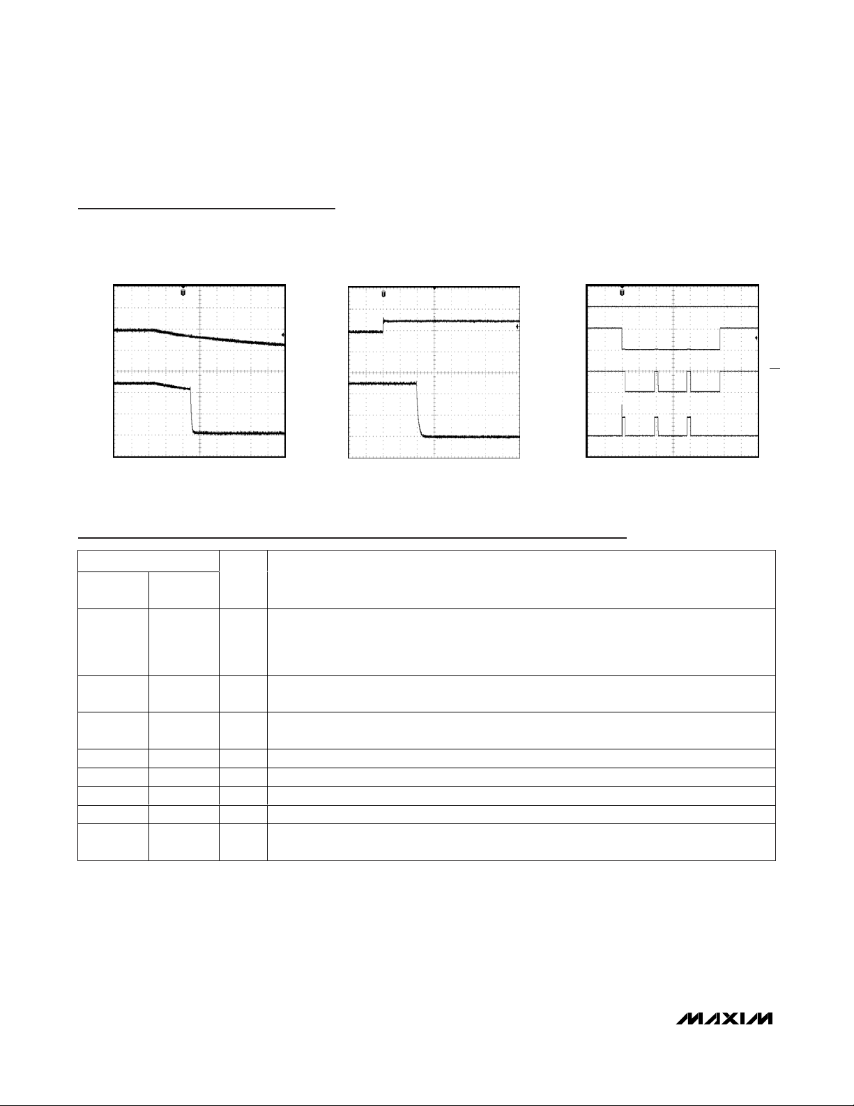
Typical Operating Characteristics
(VIN= 5.0V, EN = GND, TA= +25°C, unless otherwise noted.)
SUPPLY CURRENT
vs. SUPPLY VOLTAGE
MAX4978-81 toc01
VIN (V)
I
IN
(μA)
22 27
17
127
60
80
20
40
100
120
140
160
0
2
MAX4980/MAX4981
MAX4978
NORMALIZED ON-RESISTANCE
vs. TEMPERATURE
MAX4978-81 toc02
TEMPERATURE (°C)
NORMALIZED ON-RESISTANCE
10 60-15 35 85
1.0
0.8
0.9
1.1
1.2
1.3
0.7
-40
NORMALIZED UVLO THRESHOLD
vs. TEMPERATURE
MAX4978-81 toc03
TEMPERATURE (°C)
NORMALIZED UVLO THRESHOLD
10 60-15 35 85
1.000
0.995
1.005
1.010
0.990
-40
NORMALIZED OVLO THRESHOLD
vs. TEMPERATURE
MAX4978-81 toc04
TEMPERATURE (°C)
NORMALIZED OVLO THRESHOLD
10 60-15 35 85
1.000
0.995
1.005
1.010
0.990
-40
BATTERY OVERVOLTAGE THRESHOLD
vs. TEMPERATURE
MMAX4978-81 toc05
TEMPERATURE (°C)
BATTERY OVERVOLTAGE THRESHOLD
10 60-15 35 85
4.40
4.35
4.45
4.50
4.30
-40
NORMALIZED CURRENT LIMIT
vs. TEMPERATURE
MMAX4978-81 toc06
TEMPERATURE (°C)
NORMALIZED CURRENT LIMIT
10 60-15 35 85
1.00
0.95
1.05
1.10
0.90
-40
NORMALIZED STARTUP DELAY/AUTORETRY/
BLANKING TIME vs. TEMPERATURE
MAX4978-81 toc07
TEMPERATURE (°C)
NORMALIZED STARTUP DELAY/AUTORETRY/BLANKING TIME
10 60-15 35 85
1.000
0.996
0.998
1.004
0.994
1.002
1.006
1.008
0.992
-40
POWER-UP RESPONSE
MAX4978-81 toc08
5V/div
5V/div
5V/div
40ms/div
V
IN
V
OUT
V
SDT
OVERVOLTAGE FAULT RESPONSE
MAX4978-81 toc09
4μs/div
RL = 1kΩ
2V/div
2V/div
V
IN
V
OUT
Page 6
MAX4978–MAX4981
Overvoltage Protector with
Active Current Limit
6 _______________________________________________________________________________________
Pin Description
Typical Operating Characteristics (continued)
(VIN= 5.0V, EN = GND, TA= +25°C, unless otherwise noted.)
UNDERVOLTAGE FAULT RESPONSE
MAX4978-81 toc10
4μs/div
2V/div
2V/div
V
IN
V
OUT
BATTERY OVERVOLTAGE FAULT RESPONSE
MAX4978-81 toc11
2μs/div
RL = 1kΩ
2V/div
2V/div
V
BAT
V
OUT
SHORT-CIRCUIT RESPONSE
MAX4978-81toc12
100ms/div
5V/div
5V/div
1A/div
V
IN
V
OUT
I
OUT
V
SDT
PIN
MAX4978/
MAX4979
11IN
2—SDT
— 2 BAT
3, 6, 7 3, 6, 7 I.C. Internally Connected. Connect I.C. to GND.
44EN Acti ve- Low E nab l e Inp ut. D r i ve E N l ow for nor m al op er ati on. D r i ve E N hi g h to d i sab l e the d evi ce.
5 5 GND Ground
8 8 OUT Output Voltage. Output of internal FET.
——EP
MAX4980/
MAX4981
NAME FUNCTION
Supply Voltage Input. IN powers the charge pump required to turn on the internal FET.
When the correct adapter is plugged in, a 160ms debounce timer prevents a false turn-on of
the internal FET. Bypass IN to GND with a 1µF ceramic capacitor as close to the device as
possible to enable ±15kV (HBM) ESD protection.
Startup Debounce Time Indicator. SDT is an active-low open-drain output that asserts low
during the debounce/autoretry time.
Battery Monitor Input. Connect BAT to Li-ion battery terminal. Bypass BAT to GND with a 1µF
ceramic capacitor as close to the device as possible to enable ±15kV (HBM) ESD protection.
Exposed Pad. Internally connected to GND. Connect EP to a large ground plane to maximize
thermal performance. Do not use EP as the sole GND connection.
Page 7

MAX4978–MAX4981
Overvoltage Protector with
Active Current Limit
_______________________________________________________________________________________ 7
MAX4978/MAX4979 Functional Diagram
CONTROL
LOGIC
MAX4980
MAX4981
BANDGAP
REFERENCE
CHARGE
PUMP
+
-
+
-
+
-
OVLO
UVLO
GND
EN
OUT
IN
nFET
BAT
MAX4980/MAX4981 Functional Diagram
SDT
IN
BANDGAP
REFERENCE
OVLO
+
-
+
UVLO
-
nFET
CONTROL
LOGIC
CHARGE
PUMP
MAX4978
MAX4979
GND
OUT
EN
Page 8

MAX4978–MAX4981
Detailed Description
The MAX4978–MAX4981 family of devices is a combination of an overvoltage protector, overcurrent limiter,
and lithium-ion battery overcharge protector (MAX4980/
MAX4981). These devices feature a low 85mΩ (typ)
R
ON
FET and are used to protect the charger input port
on a portable device. If the input voltage exceeds the
overvoltage threshold (OVLO) or falls below the undervoltage threshold (UVLO), the FET is turned off to prevent damage to the protected components. The internal
charge pump’s 160ms debounce time prevents false
turn-on of the internal FET during startup. SDT is an
active-low open-drain output that asserts low during the
debounce time after a valid voltage is applied to the
input (MAX4978/MAX4979).
The MAX4978–MAX4981 feature an overcurrent limiter
as a second layer of protection for a lithium-ion battery
charger that limits current to a 900mA (MAX4978/
MAX4979/MAX4980) or 1950mA (MAX4981) threshold
for a 20ms blanking time. At the end of the blanking time,
if current is still at the threshold, the FET is turned off and
the device restarts the cycle after 160ms The battery
voltage monitor measures the voltage of a lithium-ion
battery and disables the FET if the battery voltage
exceeds 4.4V (MAX4980/MAX4981).
Autoretry
When the current-limit threshold is reached, the t
BLANK
timer begins counting. The timer resets if the overcurrent condition disappears before t
BLANK
has elapsed.
A retry time delay, t
RETRY
, is started immediately after
t
BLANK
has elapsed and during that time, the FET is off.
At the end of t
RETRY
, the FET is turned on again. If the
fault still exists, the cycle is repeated. If the fault has
been removed, the FET stays on.
Undervoltage Lockout (UVLO)
The MAX4978 has a 4.4V UVLO threshold, while the
MAX4979/MAX4980/MAX4981 have a 2.63V UVLO
threshold. When an undervoltage lockout condition
occurs with high load current, the voltage at the input to
the UVLO comparator may recover due to internal parasitic resistance causing the device to restart.
Overvoltage Lockout (OVLO)
The MAX4979 has a 6.8V OVLO threshold, while the
MAX4978/MAX4980/MAX4981 have a 5.7V OVLO
threshold.
Battery Overcharge Protector
(MAX4980/MAX4981)
The MAX4980/MAX4981 feature a battery overcharge
protection input (BAT) that triggers a voltage fault, turning off the FET, when V
BAT
exceeds 4.4V.
Startup Debounce Time Indicator (
SDT
)
(MAX4978/MAX4979)
SDT is an open-drain output that asserts low during the
startup debounce time and during the autoretry time.
SDT returns to high impedance once the charge pump
turns on. This feature is useful for discharging the AC
adapter capacitance during the startup debounce time
(Figures 1, 2).
Thermal Shutdown Protection
The MAX4978–MAX4981 have a thermal-shutdown feature to protect the devices from overheating. The
device immediately turns off when the junction temperature exceeds +160°C (typ). These devices exit thermal
shutdown after the junction temperature cools by 10°C
(typ).
EN
Input
EN is an active-low enable input. Drive EN low for normal operation. Drive EN high to disable the device.
Applications Information
IN Bypass Capacitor
For most applications, bypass IN to GND with a 1µF
ceramic capacitor as close to the device as possible to
enable ±15kV (HBM) ESD protection on IN. If the power
source has significant inductance due to long lead
length, take care to prevent overshoots due to the LC
tank circuit and provide protection if necessary to prevent exceeding the 30V absolute maximum rating on IN.
BAT Bypass Capacitor
For most applications, bypass BAT to GND with a 1µF
ceramic capacitor as close to the device as possible to
enable ±15kV (HBM) ESD protection on BAT. If high
ESD protection is not necessary, no capacitor is
required on BAT.
ESD Test Conditions
ESD performance depends on a number of conditions.
The MAX4978–MAX4981 are specified for ±15kV
(HBM) typical ESD resistance on IN and BAT when IN
and BAT are bypassed to ground with a 1µF low ESR
ceramic capacitor. Contact Maxim for a reliability report
that documents test setup, methodology, and results.
Overvoltage Protector with
Active Current Limit
8 _______________________________________________________________________________________
Page 9

Human Body Model
Figure 3 shows the Human Body Model, and Figure 4
shows the current waveform it generates when discharged into a low impedance. This model consists of
a 100pF capacitor charged to the ESD voltage of interest that is then discharged into the device through a
1.5kΩ resistor.
Chip Information
PROCESS: BiCMOS
MAX4978–MAX4981
Overvoltage Protector with
Active Current Limit
_______________________________________________________________________________________ 9
AC-DC
Figure 2. Typical Application Circuit with SDT
Figure 3. Human Body ESD Test Model
Figure 4. Human Body Current Waveform
CONVERTER
5V AC
ADAPTER
LONG WIRE
RESISTANCE
~0.5Ω
1kΩ
1μF
SDT
OVLO
UVLO
CHARGER
BANDGAP
REFERENCE
+
-
+
-
nFET
CONTROL
LOGIC
CHARGE
PUMP
MAX4978/
MAX4979
GND
OUTIN
C0NTROL
EN
PHONE
LOADS
R
D
1.5kΩ
DISCHARGE
RESISTANCE
STORAGE
CAPACITOR
DEVICE
UNDER
TEST
HIGH-
VOLTAGE
DC
SOURCE
R
C
1MΩ
CHARGE CURRENT-
LIMIT RESISTOR
C
100pF
s
AMPERES
IP 100%
90%
36.8%
10%
0
0
t
RL
I
r
TIME
t
DL
CURRENT WAVEFORM
PEAK-TO-PEAK RINGING
(NOT DRAWN TO SCALE)
Page 10

MAX4978–MAX4981
Overvoltage Protector with
Active Current Limit
Maxim cannot assume responsibility for use of any circuitry other than circuitry entirely embodied in a Maxim product. No circuit patent licenses are
implied. Maxim reserves the right to change the circuitry and specifications without notice at any time.
10
____________________Maxim Integrated Products, 120 San Gabriel Drive, Sunnyvale, CA 94086 408-737-7600
© 2008 Maxim Integrated Products is a registered trademark of Maxim Integrated Products, Inc.
Typical Application Circuit
PACKAGE TYPE PACKAGE CODE DOCUMENT NO.
8 TDFN-EP T823-1
21-0174
Package Information
For the latest package outline information and land patterns, go
to www.maxim-ic.com/packages
.
5V AC
ADAPTER
1μF
N-FET
CHARGER
OUTIN
PHONE
LOADS
BANDGAP
REFERENCE
OVLO
UVLO
+
-
+
-
-
BAT
+
CONTROL
LOGIC
CHARGE
PUMP
MAX4980
MAX4981
GND
C0NTROL
EN
 Loading...