

Page 1
19-0265; Rev 2; 9/96
Single/Dual/Quad, Micropower,
Single-Supply Rail-to-Rail Op Amps
_______________General Description
The dual MAX492, quad MAX494, and single MAX495
operational amplifiers combine excellent DC accuracy
with rail-to-rail operation at the input and output. Since
the common-mode voltage extends from VCCto VEE,
the devices can operate from either a single supply
(+2.7V to +6V) or split supplies (±1.35V to ±3V). Each
op amp requires less than 150µA supply current. Even
with this low current, the op amps are capable of driving
a 1kΩ load, and the input referred voltage noise is only
25nV/√Hz. In addition, these op amps can drive loads in
excess of 1nF.
The precision performance of the MAX492/MAX494/
MAX495, combined with their wide input and output
dynamic range, low-voltage single-supply operation, and
very low supply current, makes them an ideal choice for
battery-operated equipment and other low-voltage applications. The MAX492/MAX494/MAX495 are available in
DIP and SO packages in the industry-standard op-amp
pin configurations. The MAX495 is also available in the
smallest 8-pin SO: the µMAX package.
________________________Applications
Portable Equipment
Battery-Powered Instruments
Data Acquisition
Signal Conditioning
Low-Voltage Applications
____________________________Features
♦ Low-Voltage Single-Supply Operation (+2.7V to +6V)
♦ Rail-to-Rail Input Common-Mode Voltage Range
♦ Rail-to-Rail Output Swing
♦ 500kHz Gain-Bandwidth Product
♦ Unity-Gain Stable
♦ 150µA Max Quiescent Current per Op Amp
♦ No Phase Reversal for Overdriven Inputs
♦ 200µV Offset Voltage
♦ High Voltage Gain (108dB)
♦ High CMRR (90dB) and PSRR (110dB)
♦ Drives 1kΩ Load
♦ Drives Large Capacitive Loads
♦ MAX495 Available in µMAX Package—8-Pin SO
______________Ordering Information
PART
MAX492CPA
MAX492CSA
MAX492C/D 0°C to +70°C
MAX492EPA
MAX492ESA -40°C to +85°C
MAX492MJA -55°C to +125°C 8 CERDIP
Ordering Information continued at end of data sheet.
*
Dice are specified at TA = +25°C, DC parameters only.
TEMP. RANGE PIN-PACKAGE
0°C to +70°C
0°C to +70°C
-40°C to +85°C 8 Plastic DIP
8 Plastic DIP
8 SO
Dice*
8 SO
MAX492/MAX494/MAX495
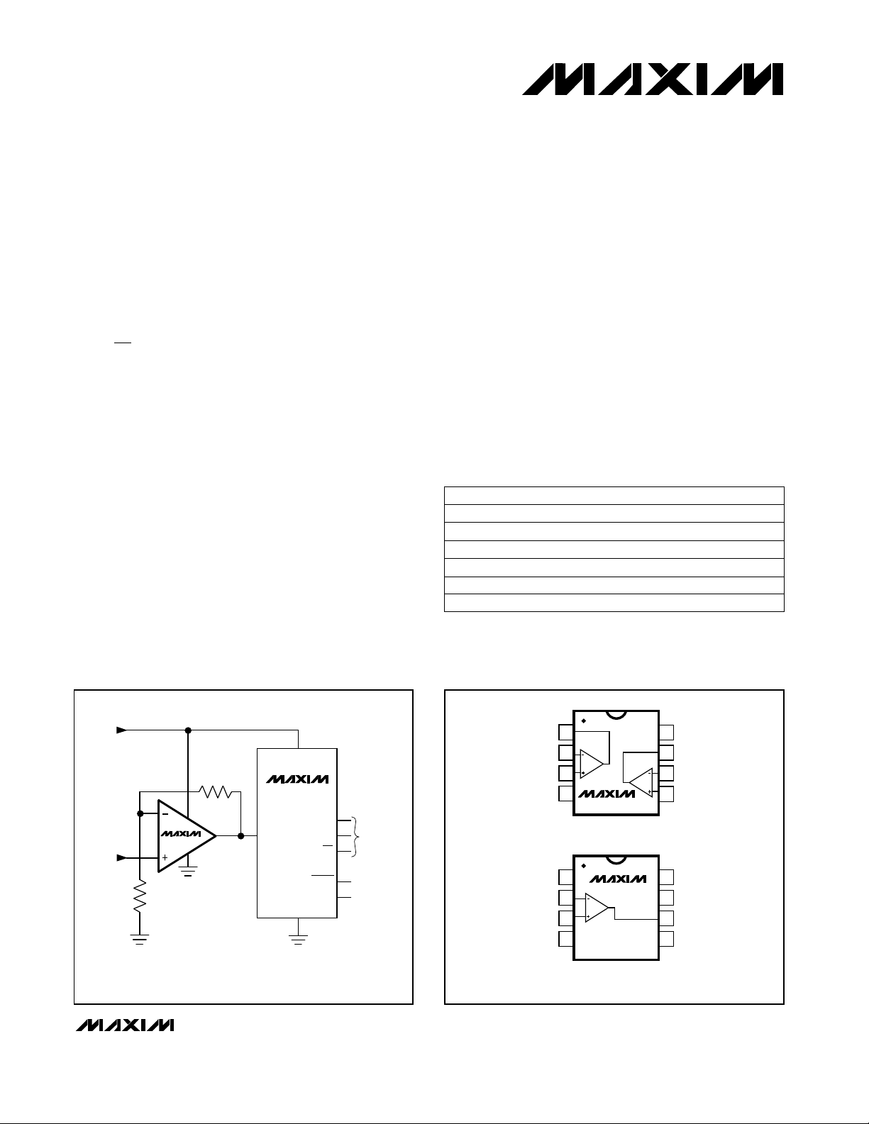
__________Typical Operating Circuit
+5V
10k
2
7
6
2
MAX495
ANALOG
INPUT
3
4
10k
INPUT SIGNAL CONDITIONING FOR LOW-VOLTAGE ADC
________________________________________________________________
AIN
1
V
DD
MAX187
(ADC)
GND
5
DOUT
SCLK
CS
SHDN
REF
6
8
7
3
4
SERIAL
INTERFACE
4.096V
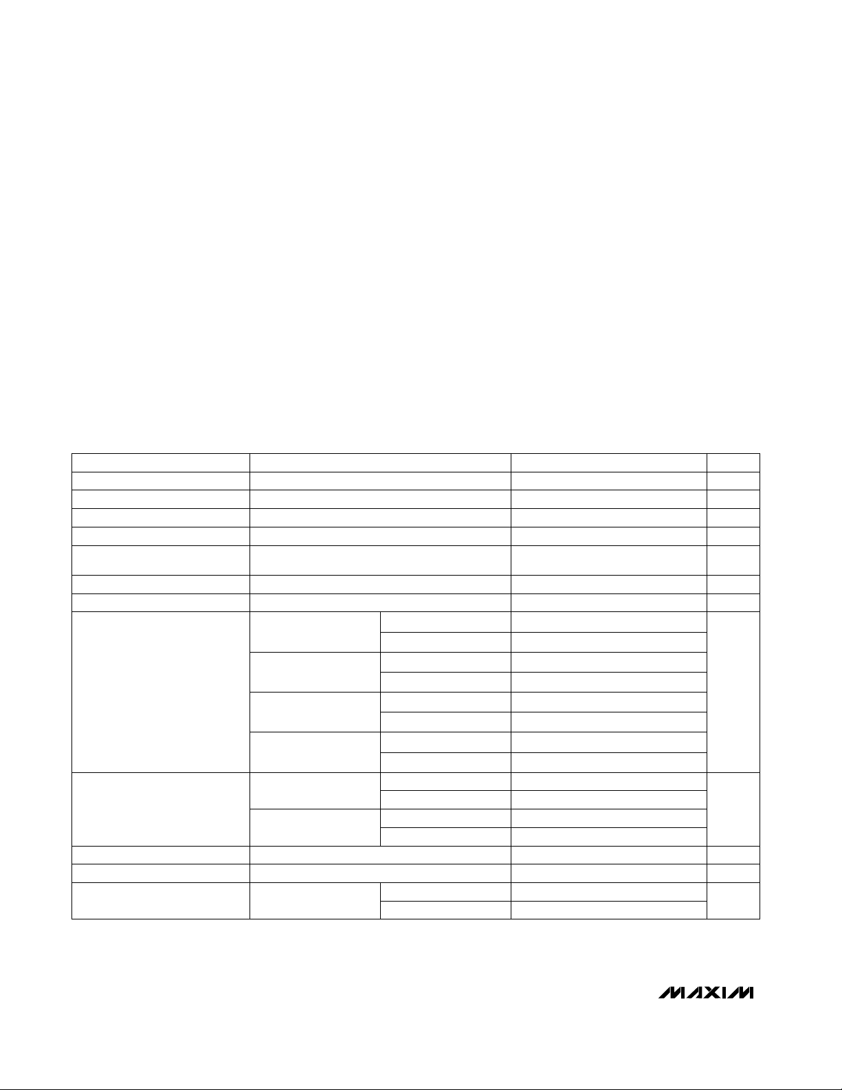
_________________Pin Configurations
TOP VIEW
OUT1
1
IN1-
2
IN1+
3
V
4
NULL
IN1-
IN1+
V
EE
EE
MAX492
DIP/SO
1
MAX495
2
3
4
DIP/SO/µMAX
Pin Configurations continued at end of data sheet.
Maxim Integrated Products
V
8
CC
OUT2
7
IN2-
6
IN2+
5
N.C.
8
V
CC
7
OUT
6
NULL
5
1
For free samples & the latest literature: http://www.maxim-ic.com, or phone 1-800-998-8800
Page 2
Single/Dual/Quad, Micropower,
Single-Supply Rail-to-Rail Op Amps
ABSOLUTE MAXIMUM RATINGS
Supply Voltage (VCCto VEE)....................................................7V
Common-Mode Input Voltage..........(V
Differential Input Voltage .........................................±(V
Input Current (IN+, IN-, NULL1, NULL2)..........................±10mA
Output Short-Circuit Duration ....................Indefinite short circuit
Voltage Applied to NULL Pins....................................V
Continuous Power Dissipation (TA= +70°C)
8-Pin Plastic DIP (derate 9.09mW/°C above +70°C) ....727mW
8-Pin SO (derate 5.88mW/°C above +70°C).................471mW
8-Pin CERDIP (derate 8.00mW/°C above +70°C).........640mW
8-Pin µMAX (derate 4.1mW/°C above +70°C)..............330mW
Stresses beyond those listed under “Absolute Maximum Ratings” may cause permanent damage to the device. These are stress ratings only, and functional
operation of the device at these or any other conditions beyond those indicated in the operational sections of the specifications is not implied. Exposure to
absolute maximum rating conditions for extended periods may affect device reliability.
+ 0.3V) to (VEE- 0.3V)
CC
CC
to either supply
CC
- VEE)
to V
EE
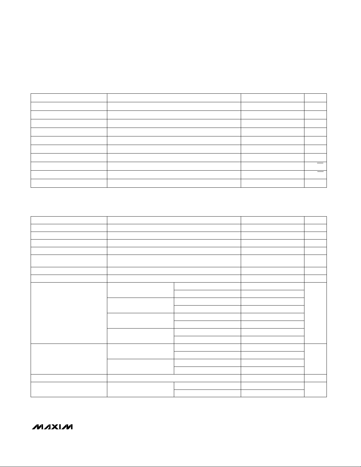
DC ELECTRICAL CHARACTERISTICS
(VCC= 2.7V to 6V, VEE= GND, VCM= 0V, V
OUT
= V
/ 2, TA= +25°C, unless otherwise noted.)
CC
14-Pin Plastic DIP (derate 10.00mW/°C above +70°C)...800mW
14-Pin SO (derate 8.33mW/°C above +70°C)...............667mW
14-Pin CERDIP (derate 9.09mW/°C above +70°C).......727mW
Operating Temperature Ranges
MAX49_C_ _ ........................................................0°C to +70°C
MAX49_E_ _......................................................-40°C to +85°C
MAX49_M_ _...................................................-55°C to +125°C
Junction Temperatures
MAX49_C_ _/E_ _..........................................................+150°C
MAX49_M_ _.................................................................+175°C
Storage Temperature Range.............................-65°C to +150°C
Lead Temperature (soldering, 10sec).............................+300°C
CONDITIONS
VCM= VEEto V
Input Bias Current
MAX492/MAX494/MAX495
Common-Mode Input
Voltage Range
Common-Mode Rejection Ratio dB
Large-Signal Voltage Gain
(Note 1)
Output Voltage Swing
(Note 1)
Supply Current (per amplifier)
VCM= VEEto V
= VEEto V
V
CM
(VEE- 0.25V) ≤ VCM≤ (VCC+ 0.25V)
VCC= 2.7V to 6V
VCC= 2.7V,
= 100kΩ,
R
L
= 0.25V to 2.45V
V
OUT
VCC= 2.7V, RL= 1kΩ,
V
= 0.5V to 2.2V
OUT
VCC= 5.0V,
= 100kΩ,
R
L
= 0.25V to 4.75V
V
OUT
VCC= 5.0V, RL= 1kΩ,
V
= 0.5V to 4.5V
OUT
RL= 100kΩ
RL= 1kΩ
VCM= V
OUT
= V
CC
CC
CC
CC
74 90
Sourcing
Sinking
Sourcing
Sinking 78 90
Sourcing
Sinking 92 100
Sourcing
Sinking 86 98
V
OH
V
OL
V
OH
V
OL
VCC= 2.7V
/ 2
VCC= 5V
90 104
90 102
94 105
98 108
98 110
VCC- 0.075 VCC- 0.04
VCC- 0.20 VCC- 0.15
VEE+ 0.04 VEE+ 0.075
VEE+ 0.15 VEE+ 0.20
135 150
150 170
UNITSMIN TYP MAXPARAMETER
µV±200 ±500Input Offset Voltage
nA±25 ±60
nA±0.5 ±6Input Offset Current
MΩ2Differential Input Resistance
VVEE- 0.25 VCC+ 0.25
dB88 110Power-Supply Rejection Ratio
dB
V
mA30Output Short-Circuit Current
V2.7 6.0Operating Supply Voltage Range
µA
2 _______________________________________________________________________________________
Page 3
Single/Dual/Quad, Micropower,
Single-Supply Rail-to-Rail Op Amps
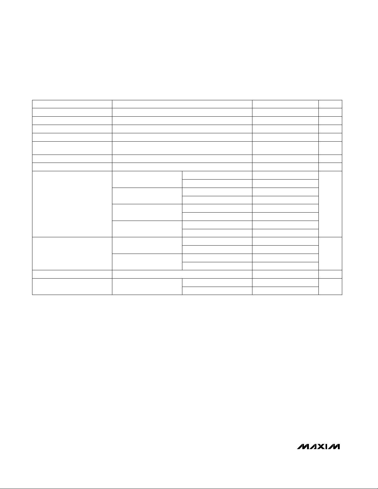
AC ELECTRICAL CHARACTERISTICS
(VCC= 2.7V to 6V, VEE= GND, TA= +25°C, unless otherwise noted.)
CONDITIONS
RL= 100kΩ, CL= 100pF
Gain Margin
Turn-On Time
Input Noise-Current Density
RL= 100kΩ, CL= 100pF
RL= 100kΩ, CL= 100pF
RL= 10kΩ, CL= 15pF, V
RL= 100kΩ, CL= 15pF
To 0.1%, 2V step
VCC= 0V to 3V step, VIN= V
f = 1kHz
f = 1kHz
f = 1kHz dB125Amp-Amp Isolation
OUT
= 2V
p-p
/ 2, AV= +1
CC
60Phase Margin
, AV= +1, f = 1kHz
5
25Input Noise-Voltage Density
degrees
DC ELECTRICAL CHARACTERISTICS
(VCC= 2.7V to 6V, VEE= GND, VCM= 0V, V
VCM= VEEto V
Input Bias Current
Common-Mode Input
Voltage Range
Common-Mode Rejection Ratio dB
Power-Supply Rejection Ratio
Large-Signal Voltage Gain
(Note 1)
Output Voltage Swing
(Note 1)
Supply Current (per amplifier)
VCM= VEEto V
VCM= VEEto V
(VEE- 0.20) ≤ VCM≤ (VCC+ 0.20)
VCC= 2.7V to 6V
VCC= 2.7V, RL= 100kΩ,
V
OUT
VCC= 2.7V, RL= 1kΩ,
V
OUT
VCC= 5.0V, RL= 100kΩ,
V
OUT
VCC= 5.0V, RL= 1kΩ,
V
OUT
RL= 100kΩ
RL= 1kΩ
VCM= V
= V
OUT
= 0.25V to 2.45V
= 0.5V to 2.2V
= 0.25V to 4.75V
= 0.5V to 4.5V
OUT
/ 2, TA= 0°C to +70°C, unless otherwise noted.)
CC
CC
CC
CC
= V
/ 2
CC
CONDITIONS
Sourcing
Sinking
Sourcing
Sinking 76
Sourcing
Sinking 88
Sourcing
Sinking
V
OH
V
OL
V
OH
V
OL
VCC= 2.7V
VCC= 5V
72
88
84
92
92
96
82
VCC- 0.075
VEE+ 0.075
VCC- 0.20
VEE+ 0.20
175
190
MAX492/MAX494/MAX495
UNITSMIN TYP MAXPARAMETER
kHz500Gain-Bandwidth Product
dB10
%0.003Total Harmonic Distortion
V/µs0.20Slew Rate
µs12Time
µs
nV/√Hz
pA/√Hz0.1
UNITSMIN TYP MAXPARAMETER
µV±650Input Offset Voltage
µV/°C±2Input Offset Voltage Tempco
nA±75
nA±6Input Offset Current
VVEE- 0.20 VCC+ 0.20
dB86
dB
V
V2.7 6.0Operating Supply Voltage Range
µA
_______________________________________________________________________________________ 3
Page 4
Single/Dual/Quad, Micropower,
Single-Supply Rail-to-Rail Op Amps
DC ELECTRICAL CHARACTERISTICS
(VCC= 2.7V to 6V, VEE= GND, VCM= 0V, V
VCM= VEEto V
Input Bias Current
Common-Mode Input
Voltage Range
Large-Signal Voltage Gain
(Note 1)
MAX492/MAX494/MAX495
Output Voltage Swing
(Note 1)
Operating Supply-Voltage Range 2.7 6.0 V
Supply Current (per amplifier) VCM= V
VCM= VEEto V
VCM= VEEto V
(VEE- 0.15) ≤ VCM≤ (VCC+ 0.15)
VCC= 2.7V to 6V, VCM= 0V
VCC= 2.7V, RL= 100kΩ,
V
OUT
VCC= 2.7V, RL= 1kΩ,
V
OUT
VCC= 5.0V, RL= 100kΩ,
V
OUT
VCC= 5.0V, RL= 1kΩ,
V
OUT
RL= 100kΩ
RL= 1kΩ
= V
OUT
= 0.25V to 2.45V
= 0.5V to 2.2V
= 0.25V to 4.75V
= 0.5V to 4.5V
OUT
/ 2, TA= -40°C to +85°C, unless otherwise noted.)
CC
CC
CC
CC
= VCC/ 2
CONDITIONS
Sourcing
Sinking
Sourcing
Sinking
Sourcing
Sinking
Sourcing
Sinking
V
OH
V
OL
V
OH
V
OL
VCC= 2.7V
VCC= 5V
±2Input Offset Voltage Tempco
68
86
84
92
76
92
86
96
80
VCC- 0.075
VEE+ 0.075
VCC- 0.20
VEE+ 0.20
185
200
UNITSMIN TYP MAXPARAMETER
µV±950Input Offset Voltage
µV/°C
nA±100
nA±8Input Offset Current
VVEE- 0.15 VCC+ 0.15
dBCommon-Mode Rejection Ratio
dB84Power-Supply Rejection Ratio
dB
V
µA
4 _______________________________________________________________________________________
Page 5
Single/Dual/Quad, Micropower,
Single-Supply Rail-to-Rail Op Amps
DC ELECTRICAL CHARACTERISTICS
(VCC= 2.7V to 6V, VEE= GND, VCM= 0V, V
VCM= VEEto V
Input Bias Current
Power-Supply Rejection Ratio
Large-Signal Voltage Gain
(Note 1)
Output Voltage Swing
(Note 1)
Supply Current (per amplifier)
VCM= VEEto V
VCM= VEEto V
(VEE- 0.05V) ≤ VCM≤ (VCC+ 0.05V)
VCC= 2.7V to 6V
VCC= 2.7V, RL= 100kΩ,
V
OUT
VCC= 2.7V, RL= 1kΩ,
V
OUT
VCC= 5.0V, RL= 100kΩ,
V
OUT
VCC= 5.0V, RL= 1kΩ,
V
OUT
RL= 100kΩ
RL= 1kΩ
VCM= V
= V
OUT
CC
CC
CC
CC
= 0.25V to 2.45V
= 0.5V to 2.2V
= 0.25V to 4.75V
= 0.5V to 4.5V
= VCC/ 2
OUT
/ 2, TA= -55°C to +125°C, unless otherwise noted.)
CONDITIONS
66
Sourcing
Sinking
Sourcing
Sinking 72
Sourcing
Sinking 82
Sourcing
Sinking
V
OH
V
OL
V
OH
V
OL
VCC= 2.7V
VCC= 5V
82
80
90
86
94
76
VCC- 0.075
VCC- 0.250
±2Input Offset Voltage Tempco
VEE+ 0.075
VEE+ 0.250
200
225
MAX492/MAX494/MAX495
UNITSMIN TYP MAXPARAMETER
mV±1.2Input Offset Voltage
µV/°C
nA±200
nA±10Input Offset Current
VVEE- 0.05 VCC+ 0.05Common-Mode Input Voltage Range
dBCommon-Mode Rejection Ratio
dB80
dB
V
V2.7 6.0Operating Supply-Voltage Range
µA
Note 1: RLto VEEfor sourcing and VOHtests; RLto VCCfor sinking and VOLtests.
_______________________________________________________________________________________ 5
Page 6
Single/Dual/Quad, Micropower,
Single-Supply Rail-to-Rail Op Amps
__________________________________________Typical Operating Characteristics
(TA = +25°C, VCC= 5V, VEE= 0V, unless otherwise noted.)
GAIN AND PHASE
80
vs. FREQUENCY
60
40
20
GAIN (dB)
0
-20
-40
0.01 10 10,000
PHASE
AV = +1000
NO LOAD
0.1 1 100 1000
GAIN
FREQUENCY (kHz)
MAX492-01
180
120
60
0
-60
-120
-180
80
60
40
20
GAIN (dB)
PHASE (DEG)
0
CL = 470pF
-20
A
R
-40
0.01 10 10,000
CHANNEL SEPARATION
vs. FREQUENCY
140
MAX492/MAX494/MAX495
120
100
80
60
40
CHANNEL SEPARATION (dB)
20
VIN = 2.5V
0
0.01 10 10,000
0.1 1 100 1000
FREQUENCY (kHz)
MAX492-04
160
140
120
100
80
60
OFFSET VOLTAGE (µV)
40
20
0
-60 -20 60 140
GAIN AND PHASE
vs. FREQUENCY
GAIN
PHASE
= +1000
V
= ∞
L
0.1 1 100 1000
FREQUENCY (kHz)
OFFSET VOLTAGE
vs. TEMPERATURE
-40 0 40 80 120
20 100
TEMPERATURE (°C)
VCM = 0V
MAX492-02
180
120
60
0
-60
-120
-180
MAX492-05
POWER-SUPPLY REJECTION RATIO
vs. FREQUENCY
140
120
100
80
60
PSRR (dB)
PHASE (DEG)
40
20
0
VIN = 2.5V
-20
0.01 10 1000
V
CC
V
EE
0.1 1 100
FREQUENCY (kHz)
COMMON-MODE REJECTION RATIO
vs. TEMPERATURE
120
VCM = 0V TO +5V
110
V
= -01V TO +5.1V
CM
100
90
CMRR (dB)
80
VCM = -0.2V TO +5.2V
= -0.3V TO +5.3V
V
CM
70
V
= -0.4V TO +5.4V
CM
60
-40 0 40 80 120
-60 -20 60 140
20 100
TEMPERATURE (°C)
MAX492-03
MAX492-06
INPUT BIAS CURRENT
vs. COMMON-MODE VOLTAGE
20
15
V
= 2.7V
CC
10
5
0
-5
-10
-15
INPUT BIAS CURRENT (nA)
-20
-25
-30
02 6
1357
VCC = 6V
4
VCM (V)
125
100
MAX492-07
75
50
25
0
-25
-50
INPUT BIAS CURRENT (nA)
-75
-100
-125
-60 0 100
INPUT BIAS CURRENT
vs. TEMPERATURE
VCC = 6V
VCM = V
CC
VCC = 2.7V
VCM = 0
VCC = 6V
-20 20 80 120
TEMPERATURE (°C)
60
SUPPLY CURRENT PER AMPLIFIER
vs. TEMPERATURE
220
V
= VCM = VCC/2
OUT
MAX492-08
140-40 40
200
180
160
140
120
100
80
60
40
SUPPLY CURRENT PER OP AMP (µA)
20
0
VCC = 5V
-40 0 40 80 120
-60 -20 60 140
TEMPERATURE (°C)
6 _______________________________________________________________________________________
MAX492-09
VCC = 2.7V
20 100
Page 7

Single/Dual/Quad, Micropower,
Single-Supply Rail-to-Rail Op Amps
____________________________Typical Operating Characteristics (continued)
(TA = +25°C, VCC= 5V, VEE= 0V, unless otherwise noted.)
200
VCC - V
RL = 1kΩ
OUT
V
(mV)
OUT
RL = 100kΩ
VCC = +6V
TO V
R
L
(mV)
R
= 100kΩ
L
RL = 10kΩ
RL = 1MΩ
EE
500
RL = 1MΩ
RL = 1kΩ
VCC = +6V
TO V
R
L
500
RL = 1MΩ
200
VCC - V
RL = 1kΩ
OUT
RL = 1MΩ
V
(mV)
OUT
RL = 100kΩ
RL = 10kΩ
VCC = +2.7V
TO V
R
L
(mV)
RL = 10kΩ
VCC = +2.7V
R
EE
500
RL = 1kΩ
TO V
L
500
LARGE-SIGNAL GAIN
vs. TEMPERATURE
120
MAX492-11
115
110
105
100
95
90
LARGE-SIGNAL GAIN (dB)
85
80
RL = 1kΩ, 0.5V < V
RL TO V
VCC = +2.7V
RL TO V
EE
-40 0 40 80 120
-60 -20 60 140
20 100
TEMPERATURE (°C)
CC
< (VCC - 0.5V)
OUT
VCC = +6V
LARGE-SIGNAL GAIN
vs. TEMPERATURE
120
MAX492-14
110
105
100
95
90
LARGE-SIGNAL GAIN (dB)
CC
85
80
RL TO V
CC
RL TO V
EE
-40 0 40 80 120
-60 -20 60 140
20 100
TEMPERATURE (°C)
RL = 100kΩ, 0.3V < V
115
< (VCC - 0.3V)
OUT
VCC = +6V
VCC = +2.7V
LARGE-SIGNAL GAIN
vs. OUTPUT VOLTAGE
120
MAX492-10
110
100
90
GAIN (dB)
80
70
60
50
0 100 300 400 600
LARGE-SIGNAL GAIN
vs. OUTPUT VOLTAGE
120
MAX492-13
110
100
90
GAIN (dB)
80
70
CC
60
50
R
= 100kΩ
L
100
0 200 300 400 600
LARGE-SIGNAL GAIN
vs. OUTPUT VOLTAGE
120
110
100
90
GAIN (dB)
80
70
60
50
RL = 10kΩ
0 100 300 400 600
LARGE-SIGNAL GAIN
vs. OUTPUT VOLTAGE
120
110
100
90
GAIN (dB)
80
70
60
50
100
0 200 300 400 600
MAX492/MAX494/MAX495
MAX492-12
MAX492-15
MINIMUM OUTPUT VOLTAGE
vs. TEMPERATURE
220
RL TO V
200
180
160
140
120
MIN (mV)
100
OUT
80
V
60
40
20
0
CC
VCC = 6V, RL = 1kΩ
VCC = 2.7V, RL = 1kΩ
VCC = 6V, RL = 100kΩ
VCC = 2.7V, RL = 100kΩ
-60 140
080
-40 -20 20 40 60 100 120
TEMPERATURE (°C)
_______________________________________________________________________________________
MAX492-16
MAXIMUM OUTPUT VOLTAGE
vs. TEMPERATURE
200
RL TO V
180
160
140
120
) (mV)
OUT
100
- V
80
CC
(V
60
40
20
0
-60 140
EE
VCC = 6V, RL = 1kΩ
VCC = 2.7V, RL = 1kΩ
VCC = 6V, RL = 100kΩ
VCC = 2.7V, RL = 100kΩ
080
-40 -20 20 40 60 100 120
TEMPERATURE (°C)
MAX492-17
OUTPUT IMPEDANCE
vs. FREQUENCY
1000
VCM = V
100
10
OUTPUT IMPEDANCE (Ω)
1
0.1
0.01 10 10,000
= 2.5V
OUT
0.1 1 100 1,000
FREQUENCY (kHz)
MAX492-18
7
Page 8

Single/Dual/Quad, Micropower,
Single-Supply Rail-to-Rail Op Amps
____________________________Typical Operating Characteristics (continued)
(TA = +25°C, VCC= 5V, VEE= 0V, unless otherwise noted.)
VOLTAGE-NOISE DENSITY
vs. FREQUENCY
100
MAX492-19
10
VOLTAGE-NOISE DENSITY (nV/√Hz)
INPUT REFERRED
1
0.01 1
0.1 10
FREQUENCY (kHz)
TOTAL HARMONIC DISTORTION + NOISE
0.1
AV = +1
MAX492/MAX494/MAX495
2V
80kHz LOWPASS FILTER
0.01
THD + NOISE (%)
0.001
10 1000
vs. FREQUENCY
SIGNAL
P-P
RL = 10kΩ TO GND
100 10,000
FREQUENCY (Hz)
MAX492-21
NO LOAD
CURRENT-NOISE DENSITY
vs. FREQUENCY
5.0
4.5
4.0
3.5
3.0
2.5
2.0
1.5
1.0
INPUT REFERRED
CURRENT-NOISE DENSITY (pA/√Hz)
0.5
0
0.01 1
0.1 10
FREQUENCY (kHz)
TOTAL HARMONIC DISTORTION + NOISE
vs. PEAK-TO-PEAK SIGNAL AMPLITUDE
0.1
AV = +1
1kHz SINE
22kHz FILTER
TO GND
R
L
0.01
THD + NOISE (%)
0.001
4.0 4.2 4.7
PEAK-TO-PEAK SIGNAL AMPLITUDE (V)
RL = 1kΩ
RL = 2kΩ
4.3 5.04.1 4.4 4.5 4.6 4.8 4.9
MAX492-20
MAX492-22
RL = 100kΩ
RL = 10kΩ
SMALL-SIGNAL TRANSIENT RESPONSE
SMALL-SIGNAL TRANSIENT RESPONSE
VIN
50mV/div
V
OUT
50mV/div
2µs/div
VCC = +5V, AV = +1, RL = 10kΩ
VCC = +5V, AV = -1, RL = 10kΩ
2µs/div
8 _______________________________________________________________________________________
VIN
50mV/div
V
OUT
50mV/div
Page 9

Single/Dual/Quad, Micropower,
Single-Supply Rail-to-Rail Op Amps
____________________________Typical Operating Characteristics (continued)
(TA = +25°C, VCC= 5V, VEE= 0V, unless otherwise noted.)
LARGE-SIGNAL TRANSIENT RESPONSE
50µs/div
V
= +5V, AV = +1, RL = 10kΩ
CC
VIN
2V/div
V
OUT
2V/div
LARGE-SIGNAL TRANSIENT RESPONSE
50µs/div
VCC = +5V, AV = -1, RL = 10kΩ
VIN
2V/div
V
OUT
2V/div
______________________________________________________________Pin Description
MAX492
4
8
PIN
MAX494
1
—
—
2
—
3
11
5
—
6
7
4
8
9
10
12
13
14
—
MAX495
—
1, 5
2
—
3
—
4
—
6
—
—
7
—
—
—
—
—
—
8
NAME
NULL—
EE
CC
Amplifier 1 OutputOUT11
Offset Null Input. Connect to a 10kΩ potentiometer for offset-voltage trimming.
Connect wiper to VEE(Figure 3).
Inverting InputIN-—
Amplifier 1 Inverting InputIN1-2
Noninverting InputIN+—
Amplifier 1 Noninverting InputIN1+3
Negative Power-Supply Pin. Connect to ground or a negative voltage.V
Amplifier 2 Noninverting InputIN2+5
Amplifier OutputOUT—
Amplifier 2 Inverting InputIN2-6
Amplifier 2 OutputOUT27
Positive Power-Supply Pin. Connect to (+) terminal of power supply.V
Amplifier 3 OutputOUT3—
Amplifier 3 Inverting InputIN3-—
Amplifier 3 Noninverting InputIN3+—
Amplifier 4 Noninverting InputIN4+—
Amplifier 4 Inverting InputIN4-—
Amplifier 4 OutputOUT4—
No Connect. Not internally connected.N.C.—
FUNCTION
MAX492/MAX494/MAX495
_______________________________________________________________________________________ 9
Page 10
Single/Dual/Quad, Micropower,
Single-Supply Rail-to-Rail Op Amps
__________Applications Information
The dual MAX492, quad MAX494, and single MAX495
op amps combine excellent DC accuracy with rail-torail operation at both input and output. With their precision performance, wide dynamic range at low supply
voltages, and very low supply current, these op amps
are ideal for battery-operated equipment and other lowvoltage applications.
Rail-to-Rail Inputs and Outputs
The MAX492/MAX494/MAX495’s input common-mode
range extends 0.25V beyond the positive and negative
supply rails, with excellent common-mode rejection.
Beyond the specified common-mode range, the outputs are guaranteed not to undergo phase reversal or
latchup. Therefore, the MAX492/MAX494/MAX495 can
be used in applications with common-mode signals at
or even beyond the supplies, without the problems
associated with typical op amps.
The MAX492/MAX494/MAX495’s output voltage swings
to within 50mV of the supplies with a 100kΩ load. This
rail-to-rail swing at the input and output substantially
increases the dynamic range, especially in low supplyvoltage applications. Figure 1 shows the input and out-
MAX492/MAX494/MAX495
put waveforms for the MAX492, configured as a
unity-gain noninverting buffer operating from a single
+3V supply. The input signal is 3.0V
centered at +1.5V. The output amplitude is approximately 2.95V
p-p
.
, 1kHz sinusoid
p-p
Input Offset Voltage
Rail-to-rail common-mode swing at the input is obtained
by two complementary input stages in parallel, which
feed a folded cascaded stage. The PNP stage is active
for input voltages close to the negative rail, and the
NPN stage is active for input voltages close to the positive rail.
The offsets of the two pairs are trimmed; however, there
is some small residual mismatch between them. This
mismatch results in a two-level input offset characteristic, with a transition region between the levels occurring
at a common-mode voltage of approximately 1.3V.
Unlike other rail-to-rail op amps, the transition region
has been widened to approximately 600mV in order to
minimize the slight degradation in CMRR caused by
this mismatch.
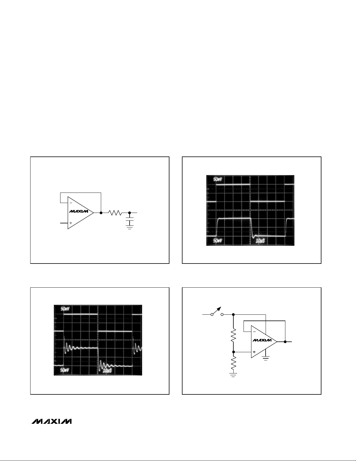
To adjust the MAX495’s input offset voltage (500µV max
at +25°C), connect a 10kΩ trim potentiometer between
the two NULL pins (pins 1 and 5), with the wiper connected to VEE(pin 4) (Figure 2). The trim range of this
circuit is ±6mV. External offset adjustment is not available for the dual MAX492 or quad MAX494.
The input bias currents of the MAX492/MAX494/MAX495
are typically less than 50nA. The bias current flows into
the device when the NPN input stage is active, and it
flows out when the PNP input stage is active. To reduce
the offset error caused by input bias current flowing
through external source resistances, match the effective resistance seen at each input. Connect resistor R3
between the noninverting input and ground when using
10k
V
IN
V
OUT
Figure 1. Rail-to-Rail Input and Output (Voltage Follower
Circuit, VCC= +3V, VEE= 0V)
10 ______________________________________________________________________________________
Figure 2. Offset Null Circuit
1
NULL
MAX495
4
V
EE
NULL
5
Page 11

Single/Dual/Quad, Micropower,
Single-Supply Rail-to-Rail Op Amps
the op amp in an inverting configuration (Figure 3a);
connect resistor R3 between the noninverting input and
the input signal when using the op amp in a noninverting configuration (Figure 3b). Select R3 to equal the
parallel combination of R1 and R2. High source resistances will degrade noise performance, due to the thermal noise of the resistor and the input current noise
(which is multiplied by the source resistance).
Input Stage Protection Circuitry
The MAX492/MAX494/MAX495 include internal protec-
tion circuitry that prevents damage to the precision
input stage from large differential input voltages. This
protection circuitry consists of back-to-back diodes
between IN+ and IN- with two 1.7kΩ resistors in series
R2
R1
V
IN
V
MAX49_
OUT
(Figure 4). The diodes limit the differential voltage
’
applied to the amplifiers
internal circuitry to no more
than VF, where VFis the diodes’forward-voltage drop
(about 0.7V at +25°C).
Input bias current for the ICs (±25nA typical) is specified for the small differential input voltages. For large
differential input voltages (exceeding VF), this protection circuitry increases the input current at IN+ and IN-:
Input Current = ———————————
2 x 1.7kΩ
(VIN+ - VIN- ) - V
F
For comparator applications requiring large differential
voltages (greater than VF), you can limit the input current that flows through the diodes with external resistors
MAX492
MAX494
MAX495
IN+
1.7kΩ
TO INTERNAL
CIRCUITRY
MAX492/MAX494/MAX495
R3
R3 = R2 II R1
Figure 3a. Reducing Offset Error Due to Bias Current:
Inverting Configuration
R3
V
IN
V
MAX49_
R3 = R2 II R1
OUT
R2
R1
Figure 3b. Reducing Offset Error Due to Bias Current:
Noninverting Configuration
______________________________________________________________________________________ 11
IN–
1.7kΩ
TO INTERNAL
CIRCUITRY
Figure 4. Input Stage Protection Circuitry
10,000
UNSTABLE REGION
1000
CAPACITIVE LOAD (pF)
100
1 10 100
RESISTIVE LOAD (kΩ)
VCC = +5V
= VCC/2
V
OUT
TO VEE
R
L
= +1
A
V
MAX492-FG 04
Figure 5. Capacitive-Load Stable Region Sourcing Current
Page 12
Single/Dual/Quad, Micropower,
Single-Supply Rail-to-Rail Op Amps
in series with IN-, IN+, or both. Series resistors are not
recommended for amplifier applications, as they may
increase input offsets and decrease amplifier bandwidth.
Output Loading and Stability
Even with their low quiescent current of less than 150µA
per op amp, the MAX492/MAX494/MAX495 are well
suited for driving loads up to 1kΩ while maintaining DC
accuracy. Stability while driving heavy capacitive loads
is another key advantage over comparable CMOS railto-rail op amps.
VIN
50mV/div
V
OUT
50mV/div
MAX492/MAX494/MAX495
10µs/div
In op amp circuits, driving large capacitive loads
increases the likelihood of oscillation. This is especially
true for circuits with high loop gains, such as a unitygain voltage follower. The output impedance and a
capacitive load form an RC network that adds a pole to
the loop response and induces phase lag. If the pole
frequency is low enough—as when driving a large
capacitive load—the circuit phase margin is degraded,
leading to either an under-damped pulse response or
oscillation.
V
IN
50mV/div
V
OUT
50mV/div
10µs/div
Figure 6. MAX492 Voltage Follower with 1000pF Load
= ∞)
(R
L
V
IN
50mV/div
V
OUT
50mV/div
10µs/div
Figure 7a. MAX492 Voltage Follower with 500pF Load—
= 5k
Ω
R
L
12 ______________________________________________________________________________________
Figure 7b. MAX492 Voltage Follower with 500pF Load—
= 20k
R
Ω
L
10µs/div
Figure 7c. MAX492 Voltage Follower with 500pF Load—
=
∞
R
L
V
IN
50mV/div
V
OUT
50mV/div
Page 13
Single/Dual/Quad, Micropower,
Single-Supply Rail-to-Rail Op Amps
The MAX492/MAX494/MAX495 can drive capacitive
loads in excess of 1000pF under certain conditions
(Figure 5). When driving capacitive loads, the greatest
potential for instability occurs when the op amp is
sourcing approximately 100µA. Even in this case, stability is maintained with up to 400pF of output capacitance. If the output sources either more or less current,
stability is increased. These devices perform well with a
1000pF pure capacitive load (Figure 6). Figure 7 shows
the performance with a 500pF load in parallel with various load resistors.
R
S
MAX49_
V
IN
V
OUT
C
L
To increase stability while driving large capacitive
loads, connect a pull-up resistor at the output to
decrease the current that the amplifier must source. If
the amplifier is made to sink current rather than source,
stability is further increased.
Frequency stability can be improved by adding an output isolation resistor (RS) to the voltage-follower circuit
(Figure 8). This resistor improves the phase margin of
the circuit by isolating the load capacitor from the op
amp’s output. Figure 9a shows the MAX492 driving
10,000pF (RL≥ 100kΩ), while Figure 9b adds a 47Ω
isolation resistor.
VIN
50mV/div
V
OUT
50mV/div
MAX492/MAX494/MAX495
Figure 8. Capacitive-Load Driving Circuit
10µs/div
Figure 9a. Driving a 10,000pF Capacitive Load
VIN
50mV/div
V
OUT
50mV/div
10µs/div
Figure 9b. Driving a 10,000pF Capacitive Load with a 47
Isolation Resistor
+5V
2
1k
3
1k
MAX495
V
CC
7
6
V
OUT
4
Figure 10. Power-Up Test Configuration
Ω
______________________________________________________________________________________ 13
Page 14

Single/Dual/Quad, Micropower,
Single-Supply Rail-to-Rail Op Amps
VCC
1V/div
V
OUT
500mV/div
VCC
2V/div
V
OUT
1V/div
5µs/div
Because the MAX492/MAX494/MAX495 have excellent
stability, no isolation resistor is required, except in the
most demanding applications. This is beneficial
because an isolation resistor would degrade the low-
MAX492/MAX494/MAX495
frequency performance of the circuit.
Power-Up Settling Time
The MAX492/MAX494/MAX495 have a typical supply
current of 150µA per op amp. Although supply current is
already low, it is sometimes desirable to reduce it further
by powering down the op amp and associated ICs for
periods of time. For example, when using a MAX494 to
buffer the inputs to a multi-channel analog-to-digital converter (ADC), much of the circuitry could be powered
down between data samples to increase battery life. If
samples are taken infrequently, the op amps, along with
the ADC, may be powered down most of the time.
When power is reapplied to the MAX492/MAX494/
MAX495, it takes some time for the voltages on the supply pin and the output pin of the op amp to settle.
Supply settling time depends on the supply voltage, the
value of the bypass capacitor, the output impedance of
the incoming supply, and any lead resistance or inductance between components. Op amp settling time
depends primarily on the output voltage and is slew-rate
limited. With the noninverting input to a voltage follower
held at mid-supply (Figure 10), when the supply steps
from 0V to VCC, the output settles in approximately 4µs
for VCC= +3V (Figure 11a) or 10µs for VCC= +5V
(Figure 11b).
5µs/div
Figure 11b. Power-Up Settling Time (VCC= +5V)Figure 11a. Power-Up Settling Time (VCC= +3V)
Power Supplies and Layout
The MAX492/MAX494/MAX495 operate from a single
2.7V to 6V power supply, or from dual supplies of
±1.35V to ±3V. For single-supply operation, bypass the
power supply with a 1µF capacitor in parallel with a
0.1µF ceramic capacitor. If operating from dual supplies, bypass each supply to ground.
Good layout improves performance by decreasing the
amount of stray capacitance at the op amp’s inputs and
output. To decrease stray capacitance, minimize both
trace lengths and resistor leads and place external
components close to the op amp’s pins.
Rail-to-Rail Buffers
The
Typical Operating Circuit
two buffer driving the analog input to a MAX187 12-bit
ADC. Both devices run from a single 5V supply, and the
converter’s internal reference is 4.096V. The MAX495’s
typical input offset voltage is 200µV. This results in an
error at the ADC input of 400µV, or less than half of one
least significant bit (LSB). Without offset trimming, the
op amp contributes negligible error to the conversion
result.
shows a MAX495 gain-of-
14 ______________________________________________________________________________________
Page 15

Single/Dual/Quad, Micropower,
Single-Supply Rail-to-Rail Op Amps
_Ordering Information (continued)
PART
MAX494CPD
MAX494CSD
MAX494EPD -40°C to +85°C
MAX494ESD
MAX494MJD -55°C to +125°C
MAX495CPA
MAX495CSA
MAX495CUA 0°C to +70°C
MAX495C/D
MAX495EPA -40°C to +85°C
MAX495ESA -40°C to +85°C 8 SO
MAX495MJA -55°C to +125°C 8 CERDIP
* Dice are specified at TA= +25°C, DC parameters only.
TEMP. RANGE PIN-PACKAGE
0°C to +70°C
0°C to +70°C
14 Plastic DIP
14 SO
14 Plastic DIP
-40°C to +85°C 14 SO
14 CERDIP
0°C to +70°C 8 Plastic DIP
0°C to +70°C
8 SO
8 µMAX
0°C to +70°C Dice*
8 Plastic DIP
____Pin Configurations (continued)
TOP VIEW
_________________Chip Topographies
MAX492
IN1+
V
CC
V
EE
V
CC
IN2+
NULL1
IN1-
IN2-
0.069"
(1.752mm)
MAX495
OUT1
0.068"
(1.728mm)
V
CC
OUT2
MAX492/MAX494/MAX495
OUT1
IN1IN1+
V
IN2+
IN2-
OUT2
IN-
1
2
3
CC
4
MAX494
5
6
7
DIP/SO
OUT4
14
IN4-
13
IN4+
12
V
11
EE
IN3+
10
IN3-
9
OUT3
8
IN+
V
EE
0.055"
(1.397mm)
NULL2
V
CC
0.056"
(1.422mm)
OUT
TRANSISTOR COUNT: 134 (single MAX495)
268 (dual MAX492)
536 (quad MAX494)
SUBSTRATE CONNECTED TO V
______________________________________________________________________________________ 15
EE
Page 16
Single/Dual/Quad, Micropower,
Single-Supply Rail-to-Rail Op Amps
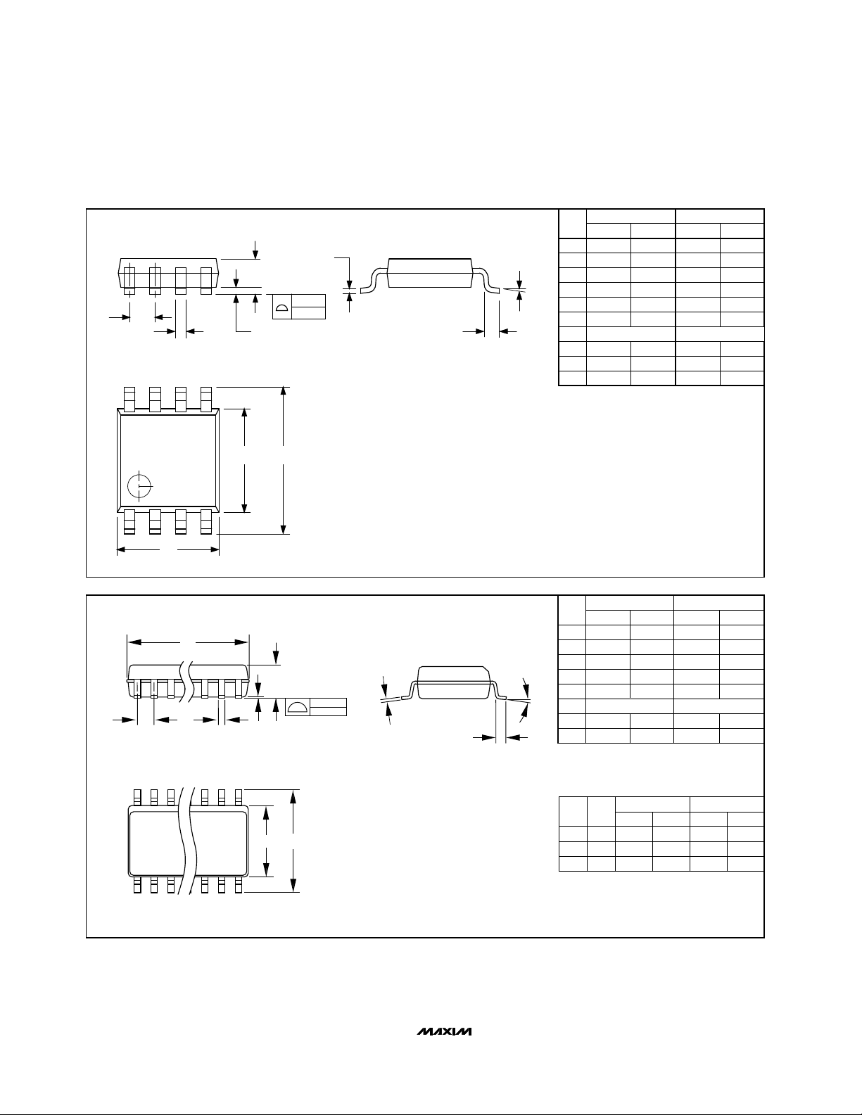
________________________________________________________Package Information
C
A
0.101mm
e
A1B
E H
0.004 in
8-PIN µMAX
MICROMAX SMALL-OUTLINE
PACKAGE
MAX492/MAX494/MAX495
D
D
A
0.101mm
e
A1
B
0.004in.
C
DIM
α
L
A1
DIM
A1
0°-8°
L
INCHES MILLIMETERS
MIN
A
0.036
0.004
B
0.010
C
0.005
D
0.116
E
0.116
e
H
0.188
L
0.016
α
MIN
A
0.053
0.004
B
0.014
C
0.007
E
0.150
e
H
0.228
L
0.016
MAX
0.044
0.008
0.014
0.007
0.120
0.120
0°
INCHES MILLIMETERS
0.198
0.026
6°
MAX
0.069
0.010
0.019
0.010
0.157
0.244
0.050
MIN
0.91
0.10
0.25
0.13
2.95
2.95
4.78
0.41
0°
MIN
1.35
0.10
0.35
0.19
3.80
5.80
0.40
MAX
1.11
0.20
0.36
0.18
3.05
3.05
0.650.0256
5.03
0.66
6°
21-0036D
MAX
1.75
0.25
0.49
0.25
4.00
1.270.050
6.20
1.27
PINS
Narrow SO
HE
SMALL-OUTLINE
PACKAGE
(0.150 in.)
Maxim cannot assume responsibility for use of any circuitry other than circuitry entirely embodied in a Maxim product. No circuit patent licenses are
implied. Maxim reserves the right to change the circuitry and specifications without notice at any time.
16
__________________Maxim Integrated Products, 120 San Gabriel Drive, Sunnyvale, CA 94086 (408) 737-7600
DIM
D
D
D
INCHES MILLIMETERS
MIN
MAX
8
0.189
0.197
14
0.337
0.344
16
0.386
0.394
MIN
4.80
8.55
9.80
MAX
5.00
8.75
10.00
21-0041A
© 1996 Maxim Integrated Products Printed USA is a registered trademark of Maxim Integrated Products.
 Loading...