

Page 1
MAX4910/MAX4911/MAX4912
Quad-SPDT, Clickless Audio Switches
with Negative Signal Handling
________________________________________________________________ Maxim Integrated Products 1
19-3854; Rev 0; 2/06
For pricing, delivery, and ordering information, please contact Maxim/Dallas Direct! at
1-888-629-4642, or visit Maxim’s website at www.maxim-ic.com.
15
16
14
13
5
6
7
8
COM4 NO4 EN NC3
NC1 CB NO2 COM2
13
V
CC
4
12 10 9
NO1
COM1
COM3
NO3
GND
NC2
MAX4911
2
11
NC4
THIN QFN
3 mm x 3 mm
+
15
16
14
13
5
6
7
8
COM4 NO4 CB2 NC3
NC1 CB1 NO2 COM2
13
V
CC
4
12 10 9
NO1
COM1
COM3
NO3
GND
NC2
MAX4910
MAX4912
2
11
NC4
THIN QFN
3 mm x 3 mm
TOP VIEW
+
Pin Configurations
General Description
The MAX4910/MAX4911/MAX4912 quad, singlepole/double-throw (SPDT), clickless audio switches feature negative signal capability that allows signals as low
as VCC-5.5V to pass through without distortion. These
analog switches have a low on-resistance, low supply
current, and operate from a single +1.8V to +5.5V supply.
The MAX4910/MAX4911/MAX4912 have internal shunt
resistors that automatically discharge the capacitance at
the normally open (NO) and normally closed (NC) terminals when they are not connected. The MAX4910/
MAX4911 have shunt resistors on all NO and NC terminals
and the MAX4912 has shunt resistors on all NO, NC1, and
NC3 terminals. These shunt resistors reduce click-andpop sounds that occur when switching audio signals
between precharged points. A break-before-make feature
further reduces popping.
The MAX4910/MAX4912 control the switches in pairs with
two control bits CB1 and CB2. The MAX4911 has one control bit to switch all four switches and an enable pin EN to
put the switches in a high-impedance mode. The MAX4912
has two terminals without shunt resistors for switching
applications that do not require pre-discharge switching.
The MAX4910/MAX4911/MAX4912 are available in a tiny
16-pin TQFN-EP (3mm x 3mm) package and operate
over the -40°C to +85°C extended temperature range.
Applications
Cell Phones
PDAs and Handheld Devices
Notebook Computers
MP3 Players
Features
♦ Distortion-Free Negative Signal Throughput Down
to VCC- 5.5V
♦ Internal Shunt Resistors Reduce Click-and-Pop
Sounds
♦ High PSRR Reduces Supply Noise
♦ Low On-Resistance (0.37Ω)
♦ 0.1Ω Channel-to-Channel Matching
♦ 0.35Ω On-Resistance Flatness
♦ +1.8V to +5.5V Single-Supply Voltage
♦ -80dB Crosstalk (20kHz)
♦ -90dB Off-Isolation (20kHz)
♦ 0.05% Total Harmonic Distortion
♦ Enable Control (MAX4911)
♦ 10nA Leakage Current
♦ 150nA Supply Current
Ordering Information
PA RT
T EM P R AN G E
PINPA CK A G E
T O P
PK G
C O DE
M A X4 9 1 0E TE+
T1633- 4
M A X4 9 1 1E TE+ *
T1633- 4
M A X4 9 1 2E TE+ *
T1633- 4
+ Denotes lead-free package.
*Future product—contact factory for availability.
**EP = Exposed pad.
Typical Operating Circuit appears at end of data sheet.
M A RK
- 40°C to + 85°C 16 TQFN- E P ** AD Y
- 40°C to + 85°C 16 TQFN- E P ** AD Z
- 40°C to + 85°C 16 TQFN- E P ** AE A
Page 2
MAX4910/MAX4911/MAX4912
Quad-SPDT, Clickless Audio Switches
with Negative Signal Handling
2 _______________________________________________________________________________________
ABSOLUTE MAXIMUM RATINGS
ELECTRICAL CHARACTERISTICS
(VCC= +2.7V to +5.5V, TA= -40°C to +85°C, EN = low (MAX4911 only), unless otherwise noted. Typical values are at VCC= +3.0V, TA=
+25°C.) (Note 1)
Stresses beyond those listed under “Absolute Maximum Ratings” may cause permanent damage to the device. These are stress ratings only, and functional
operation of the device at these or any other conditions beyond those indicated in the operational sections of the specifications is not implied. Exposure to
absolute maximum rating conditions for extended periods may affect device reliability.
(All voltages referenced to GND.)
V
CC
, CB_, EN ........................................................-0.3V to +6.0V
COM_, NC_, NO_ ...............................(V
CC
- 6V) to (VCC+ 0.3V)
Continuous Current NO_, NC_, COM_ ...........................±300mA
Peak Current NO_, NC_, COM_ (pulsed at 1ms,
50% duty cycle)..........................................................±400mA
Peak Current NO_, NC_, COM_ (pulsed at 1ms,
10% duty cycle)..........................................................±500mA
Continuous Power Dissipation (T
A
= +70°C)
16-Pin TQFN, Single-Layer Board
(derate 15.6mW/°C above +70°C).............................1250mW
16-Pin TQFN, Multilayer Board
(derate 20.8mW/°C above +70°C).............................1667mW
Operating Temperature Range ...........................-40°C to +85°C
Junction Temperature......................................................+150°C
Storage Temperature Range .............................-65°C to +150°C
Lead Temperature (soldering, 10s) .................................+300°C
PARAMETER
SYMBOL
CONDITIONS
MIN
TYP
MAX
UNITS
POWER SUPPLY
Supply Voltage V
CC
1.8 5.5 V
VCC = +5.5V, V
CB_
= VEN = 0V or V
CC
2
VCC = +2.7V, V
CB_
= VEN = +0.5V or +1.4V 4Supply Current I
CC
VCC = +5.5V, V
CB_
= VEN = +0.5V or +1.4V 8
µA
ANALOG SWITCH
Analog Signal Range
V
NC
_,
V
NO
_,
(Note 2)
V
CC
V
TA = +25°C
C hannel s 1 and 3, V
C C
=
+ 3.3V , V
N C _
or V
N O_
= V
C C
-
5.5V , - 1V , 0V , + 1V , + 2V , V
C C
,
I
C OM 1
= I
C OM 3
= 100m A
T
A
= T
MIN
to T
MAX
0.8
Ω
TA = +25°C
On-Resistance
(Note 3)
R
ON
C hannel s 2 and 4, V
C C
=
+ 3.3V , V
N C _
or V
N O_
= V
C C
-
5.5V , - 1V , 0V , + 1V , + 2V , V
C C
,
I
C OM 2
= I
C OM 4
= 100m A
T
A
= T
MIN
to T
MAX
1.6
Ω
Channels 1 and 3, VCC = +3.3V, V
NC_
or V
NO_
= 0,
I
COM_
= 100mA
0.1
On-Resistance Match
Between Channels
(Notes 3, 4)
∆R
ON
Channels 2 and 4, VCC = +3.3V, V
NC_
or V
NO_
= 0,
I
COM_
= 100mA
0.1
Ω
C hannel s 1 and 3, V
C C
= +3.3V , V
N C _
= V
N O_
=
On-Resistance Flatness
(Note 5)
R
FLAT
C hannel s 2 and 4, V
C C
= +3.3V , V
N C _
= V
N O_
=
0.6
Ω
Shunt Switch Resistance R
SH
2 3.8 6 kΩ
0.15
V
COM
_,
V
- 5.5V , - 1V , 0V , + 1V , + 2V , V
C C
V
- 5.5V , - 1V , 0V , + 1V , + 2V , V
C C
C C
C C
, I
= 100m A
C OM _
, I
= 100m A
C OM _
5.5V
0.37 0.75
0.72 1.45
V
CC
0.35
Page 3
MAX4910/MAX4911/MAX4912
Quad-SPDT, Clickless Audio Switches
with Negative Signal Handling
_______________________________________________________________________________________ 3
Note 1: All parameters are production tested at TA= +85°C and guaranteed by design over the specified temperature range.
Note 2: Signals on COM_, NO_, or NC_ exceeding V
CC
are clamped by internal diodes. Limit forward-diode current to maximum current
rating.
Note 3: Guaranteed by design; not production tested.
Note 4: ∆R
ON
= R
ON(MAX)
- R
ON(MIN)
.
Note 5: Flatness is defined as the difference between the maximum and minimum value of on-resistance as measured over the specified
analog signal ranges.
Note 6: Off-isolation = 20log
10[VCOM_
/ V
NO_
], V
COM_
= output, VNO_ = input to off switch.
ELECTRICAL CHARACTERISTICS (continued)
(VCC= +2.7V to +5.5V, TA= -40°C to +85°C, EN = low (MAX4911 only), unless otherwise noted. Typical values are at VCC= +3.0V, TA=
+25°C.) (Note 1)
PARAMETER
SYMBOL
CONDITIONS
MIN
TYP
MAX
UNITS
TA = +25°C
NC_ Off-Leakage Current
)
MAX4912 (NC2 and NC4)
only: V
CC
= +2.7V, switch
open, V
NC_
= -2.5V or
+2.5V, V
COM_
= +2.5V or
-2.5V
T
A
= T
MIN
to T
MAX
nA
TA = +25°C
COM_ On-Leakage Current
)
VCC = +2.7V, switch closed;
V
NC_
or V
NO_
= -2.5V,
+2.5V, or floating; V
COM_
=
-2.5V, +2.5V, or floating
T
A
= T
MIN
to T
MAX
nA
DYNAMIC CHARACTERISTICS
Turn-On Time t
ON
VCC = +2.7V, CB_ = low to high, RL = 50Ω,
C
L
= 5pF, V
NO_
= +1.5V, Figure 2
µs
Turn-Off Time t
OFF
VCC = +2.7V, CB_ = high to low, RL = 50Ω,
C
L
= 5pF, V
NO_
= +1.5V, Figure 2
0.3 1.0 µs
Break-Before-Make Delay
Time
t
D
V
C C
= + 2.7V , C B_ = l ow to hi g h or hi g h to l ow ,
125 ns
Charge Injection Q V
GEN_
= 0, R
GEN
= 0, CL = 1nF, Figure 4
pC
P ow er - S up p l y Rej ecti on Rati o
PSRR f = 20kHz, V
COM_
= 1V
RMS, RL
= 50Ω, CL = 5pF 60 dB
Off-Isolation V
ISO
f = 20kHz, V
COM_
= 1V
RMS
, RL = 50Ω, Figure 5
(Note 6)
dB
Crosstalk V
CT
f = 20kHz, V
COM_
= 1V
RMS
, RL = 50Ω, Figure 5
dB
Total Harmonic Distortion THD
f = 20Hz to 20kHz, V
COM_
= 0.5V
P-P
, RL = 50Ω,
DC bias = 0
%
NO_, NC_ Off-Capacitance
(
)
f = 1M H z, V
C OM _
= 0.5V
P - P ,
D C b i as = 0, Fi g ur e 6
pF
COM On-Capacitance
(ON)
f = 1M H z, V
C OM _
= 0.5V
P - P
, D C b i as = 0, Fi g ur e 6
pF
DIGITAL INPUTS (CB_, EN)
Input Logic High V
IH
1.4 V
Input Logic Low V
IL
0.5 V
Input Leakage Current
VCB_ = VEN = 0V or V
CC
-1 +1 µA
I
NC_(OFF
I
COM_(ON
RL = 50Ω , C L = 5p F, V
N C _
= V
CNO_
C
OFF
_
COM
ICB, I
EN
= + 1.5V , Fi g ur e 3
N O_
-10 +10
-50 +50
-10 +10
-100 +100
0.055 0.15
300
-90
-80
0.05
100
200
Page 4
MAX4910/MAX4911/MAX4912
Quad-SPDT, Clickless Audio Switches
with Negative Signal Handling
4 _______________________________________________________________________________________
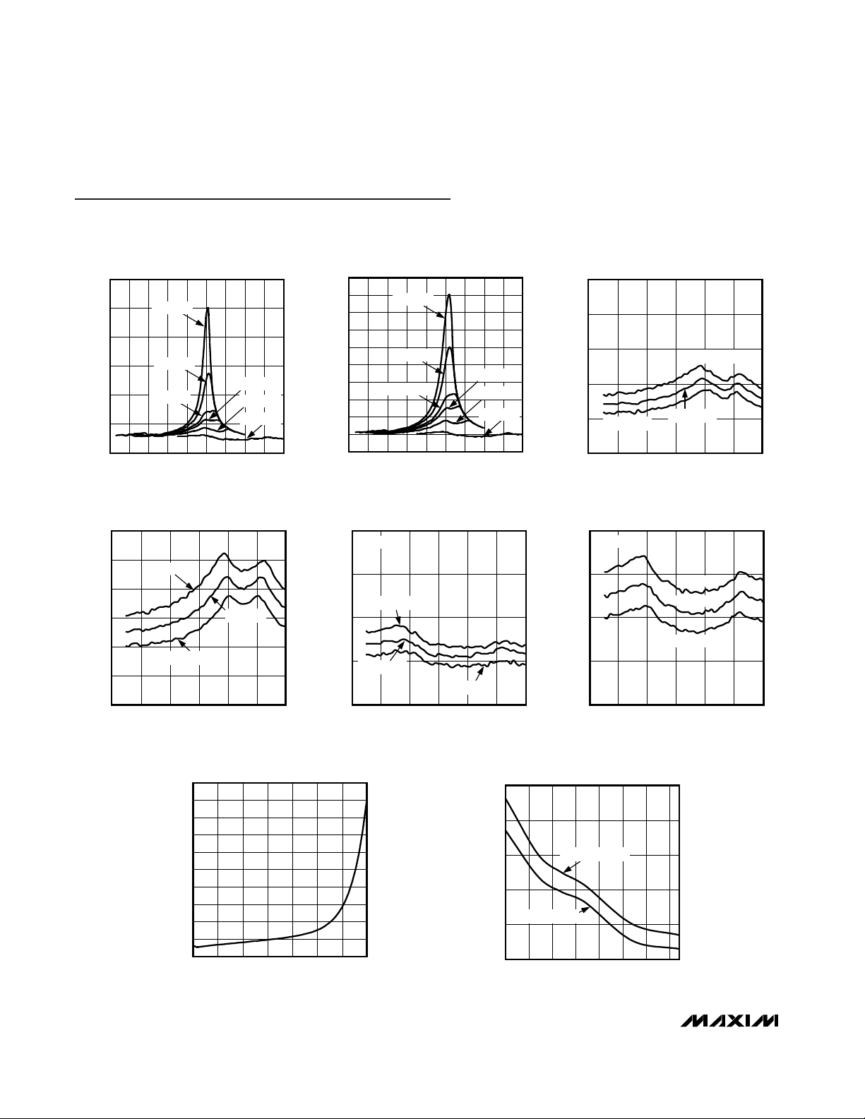
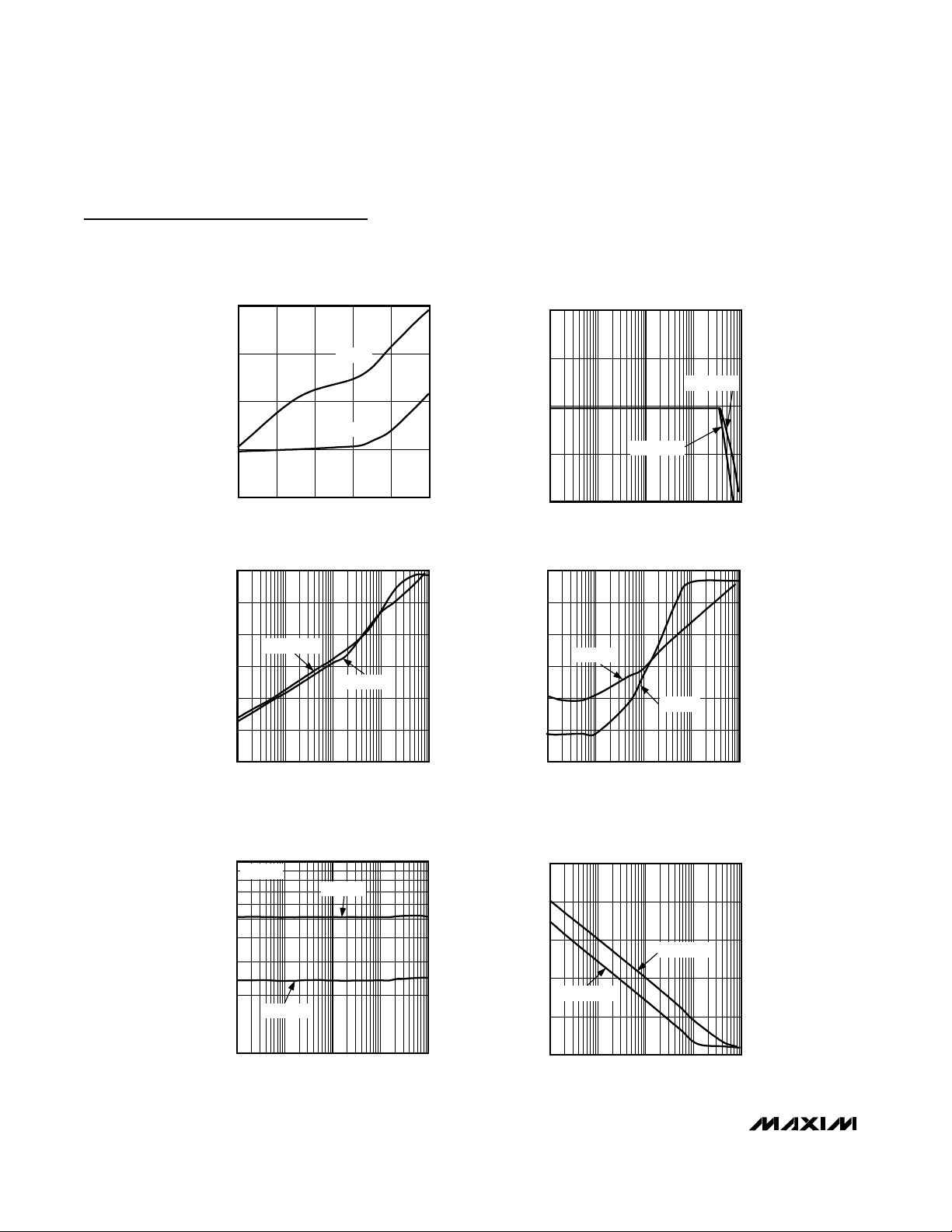
Typical Operating Characteristics
(V
CC
= 3.0V, TA = +25°C, unless otherwise noted.)
0
0.5
1.0
1.5
2.0
2.5
3.0
-4 -2-3 -1 012345
CHANNEL 1/3 ON-RESISTANCE
vs. COM 1/3 VOLTAGE
MAX4910/11/12 toc01
COM VOLTAGE (V)
ON-RESISTANCE (Ω)
VCC = 1.8V
VCC = 2.0V
VCC = 2.3V
VCC = 3.0V
VCC = 2.5V
VCC = 5.0V
0
1.0
0.5
2.0
1.5
3.0
2.5
3.5
4.5
4.0
5.0
-4 -2 -1 0-3 12345
CHANNEL 2/4 ON-RESISTANCE
vs. COM 2/4 VOLTAGE
MAX4910/11/12 toc02
COM VOLTAGE (V)
ON-RESISTANCE (Ω)
VCC = 1.8V
VCC = 2.0V
VCC = 2.3V
VCC = 3.0V
VCC = 2.5V
VCC = 5.0V
0
0.2
0.6
0.4
0.8
1.0
-3 -1-2 0 123
CHANNEL 1/3 ON-RESISTANCE
vs. COM 1/3 VOLTAGE
MAX4910/11/12 toc03
COM VOLTAGE (V)
ON-RESISTANCE (Ω)
TA = +85°C
TA = +25°C
TA = -40°C
0
0.4
0.2
0.8
0.6
1.0
1.2
-3 -1 0-2 123
CHANNEL 2/4 ON-RESISTANCE
vs. COM 2/4 VOLTAGE
MAX4910/11/12 toc04
COM VOLTAGE (V)
ON-RESISTANCE (Ω)
TA = +85°C
TA = +25°C
TA = -40°C
0.8
0.6
0.4
0.2
0
-1 201 34 5
CHANNEL 1/3 ON-RESISTANCE
vs. COM 1/3 VOLTAGE
MAX4910/11/12 toc05
COM VOLTAGE (V)
ON-RESISTANCE (Ω)
TA = +85°C
TA = +25°C
TA = -40°C
VCC = 5.0V
0.8
0.6
0.4
0.2
0
-1 201 34 5
CHANNEL 2/4 ON-RESISTANCE
vs. COM 2/4 VOLTAGE
MAX4910/11/12 toc06
COM VOLTAGE (V)
ON-RESISTANCE (Ω)
TA = +85°C
TA = +25°C
TA = -40°C
VCC = 5.0V
0
60
40
20
100
80
180
160
140
120
200
1.8 2.3 2.8 3.3 3.8 4.3 4.8 5.3
SUPPLY CURRENT vs. SUPPLY VOLTAGE
MAX4910/11/12 toc07
SUPPLY VOLTAGE (V)
SUPPLY CURRENT (nA)
200
250
350
300
400
450
1.8 2.8 3.32.3 3.8 4.3 4.8 5.3
NC TURN-ON / NO TURN-OFF TIME
vs. SUPPLY VOLTAGE
MAX4910/11/12 toc08
SUPPLY VOLTAGE (V)
TURN-ON/TURN-OFF TIME (ns)
NC TURN-ON TIME
NO TURN-OFF TIME
Page 5

MAX4910/MAX4911/MAX4912
Quad-SPDT, Clickless Audio Switches
with Negative Signal Handling
_______________________________________________________________________________________ 5
Typical Operating Characteristics (continued)
(V
CC
= 3.0V, TA = +25°C, unless otherwise noted.)
10
30
20
60
50
40
90
80
70
100
1.8 3.3 3.82.3 2.8 4.3 4.8 5.3
NO TURN-ON/NC TURN-OFF TIME
vs. SUPPLY VOLTAGE
MAX4910/11/12 toc09
SUPPLY VOLTAGE (V)
TURN-ON/TURN-OFF TIME (ns)
NO TURN-ON TIME
NC TURN-OFF TIME
0
20
10
40
30
60
50
70
90
80
100
-40 -10 5 20-25 35 50 65 80
NO TURN-ON/NC TURN-OFF TIME
vs. TEMPERATURE
MAX4910/11/12 toc10
TEMPERATURE (°C)
TURN-ON/TURN-OFF TIME (ns)
NC TURN-OFF TIME
NO TURN-ON TIME
270
290
280
310
300
330
320
340
360
350
370
-40 -10 5 20-25 35 50 65 80
NC TURN-ON/NO TURN-OFF TIME
vs. TEMPERATURE
MAX4910/11/12 toc11
TEMPERATURE (°C)
TURN-ON/TURN-OFF TIME (ns)
NO TURN-OFF TIME
NC TURN-ON TIME
0
0.4
1.2
0.8
1.6
2.0
1.8 2.8 3.32.3 3.8 4.3 4.8 5.3
LOGIC THRESHOLD
vs. SUPPLY VOLTAGE
MAX4910/11/12 toc12
SUPPLY VOLTAGE (V)
LOGIC THRESHOLD (V)
VCB RISING
VCB FALLING
2.0
1.5
1.0
0.5
0
0312 41.4 5
SUPPLY CURRENT
vs. LOGIC INPUT VOLTAGE
MAX4910/11/12 toc13
DIGITAL INPUT VOLTAGE (V)
SUPPLY CURRENT (µA)
0.5
VCC = +4.3V
-300
-100
100
300
500
700
900
-3 -1-2 012345
CHARGE INJECTION
vs. COMMON VOLTAGE
MAX4910/11/12 toc14
V
COM
(V)
CHARGE INJECTION (pC)
VCC = 5.0V
VCC = 2.0V
Page 6
MAX4910/MAX4911/MAX4912
Quad-SPDT, Clickless Audio Switches
with Negative Signal Handling
6 _______________________________________________________________________________________
TOTAL HARMONIC DISTORTION
vs. FREQUENCY
MAX4910/11/12 toc19
FREQUENCY (kHz)
THD (%)
1010.10.01 100
0.1
0.01
THD COM
THD COM
RL = 50Ω
CHANNEL 2/3 POWER SUPPLY
REJECTION RATIO vs. FREQUENCY
MAX4910/11/12 toc20
FREQUENCY (MHz)
PSRR (dB)
1010.1
20
40
60
80
100
0
0.01 100
CHANNEL 2/3
CHANNEL 1/4
OFF-ISOLATION vs. FREQUENCY
MAX4910/11/12 toc17
FREQUENCY (MHz)
ON-LOSS (dB)
1010.1
-100
-80
-60
-40
-20
0
-120
0.01 100
CHANNEL 2/4
CHANNEL 1/3
CROSSTALK vs. FREQUENCY
MAX4910/11/12 toc18
FREQUENCY (MHz)
ON-LOSS (dB)
1010.1
-100
-80
-60
-40
-20
0
-120
0.01 100
COM 2/4
COM 1/3
FREQUENCY RESPONSE
MAX4910/11/12 toc16
FREQUENCY (MHz)
ON-LOSS (dB)
1010.1
-3
0
3
6
-6
0.01 100
CHANNEL 2/4
CHANNEL 1/3
LEAKAGE CURRENT
vs. TEMPERATURE
MAX4910/11/12 toc15
TEMPERATURE (°C)
LEAKAGE CURRENT (pA)
603510-15
10
100
1000
10,000
1
-40 85
I
COM(ON)
I
COM(OFF)
Typical Operating Characteristics (continued)
(V
CC
= 3.0V, TA = +25°C, unless otherwise noted.)
Page 7

MAX4910/MAX4911/MAX4912
Quad-SPDT, Clickless Audio Switches
with Negative Signal Handling
_______________________________________________________________________________________ 7
Detailed Description
The MAX4910/MAX4911/MAX4912 quad SPDT audio
switches are low on-resistance, low supply current,
high power-supply rejection ratio (PSRR) devices that
operate from a +1.8V to +5.5V single supply. These
devices feature a negative signal capability that allows
signals below GND to pass through without distortion
and break-before-make switching.
The MAX4910/MAX4912 have two digital control inputs
CB1 and CB2 where each bit controls a pair of switches (see Table 1). The MAX4911 has an active-low
enable EN and a digital control bit CB. Driving EN low
takes the switches out of high impedance and CB controls all four switches (see Table 2). The MAX4910/
MAX4911 have shunt resistors on all their NO and NC
terminals to suppress click-and-pop sounds that may
occur from switching to a precharged terminal. The
MAX4912 does not have click-and-pop suppression
resistors on NC2 and NC4 for applications that do not
require predischarge switching.
Pin Description
PIN
MAX4910/
MAX4912
NAME FUNCTION
11NC1 Analog Switch 1—Normally Closed Terminal
2—CB1 Digital Control Input for Analog Switch 1 and Analog Switch 3
—2CB Digital Control Input for All Analog Switches
33NO2 Analog Switch 2—Normally Open Terminal
44COM2 Analog Switch 2—Common Terminal
55NC2 Analog Switch 2—Normally Closed Terminal
66GND Ground
77NO3 Analog Switch 3—Normally Open Terminal
88COM3 Analog Switch 3—Common Terminal
99NC3 Analog Switch 3—Normally Closed Terminal
10 — CB2 Digital Control Input for Analog Switch 2 and Analog Switch 4.
—10EN
Enable Input. Driving EN high causes all switches to be high impedance. Pull EN low for
normal operation.
11 11 NO4 Analog Switch 4—Normally Open Terminal
12 12 COM4 Analog Switch 4—Common Terminal
13 13 NC4 Analog Switch 4—Normally Closed Terminal
14 14 V
CC
Positive Supply Voltage Input
15 15 NO1 Analog Switch 1—Normally Open Terminal
16 16 COM1 Analog Switch 1—Common Terminal
——EP Exposed Pad. Connect to Ground
Table 1. MAX4910/MAX4912 Truth Tables
CB1 NC1 NO1 NC3 NO3
0OnOffOn Off
1OffOnOff On
CB2 NC2 NO2 NC4 NO4
0OnOffOn Off
1OffOnOff On
Table 2. MAX4911 Truth Table
EN CB NC_ NO_
1XOffOff
01OffOn
00OnOff
X = Don’t care.
MAX4911
Page 8

MAX4910/MAX4911/MAX4912
Quad-SPDT, Clickless Audio Switches
with Negative Signal Handling
8 _______________________________________________________________________________________
Applications Information
Digital Control Inputs
The MAX4910/MAX4911/MAX4912 logic inputs accept
up to +5.5V, regardless of supply voltage. For example,
with a +3.3V supply, CB1, CB2, CB, and EN can be dri-
ven low to GND and high to +5.5V, allowing for mixed
logic levels in a system. Driving CB, CB1, CB2, and EN
rail-to-rail minimizes power consumption. For a +3.3V
supply voltage, the logic thresholds are +0.5V (low)
and +1.4V (high).
GND
MAX4910
V
CC
CB1
CB2
CONTROL
LOGIC
CB1 = 0, CB2 = 0.
NO3
NC3
COM3
NC2
NO2
COM2
NC4
NO4
COM4
NO1
NC1
COM1
GND
MAX4912
V
CC
CB1
CB2
CONTROL
LOGIC
CB1 = 0, CB2 = 0.
NO3
NC3
COM3
NC2
NO2
COM2
NC4
NO4
COM4
NO1
NC1
COM1
GND
MAX4911
V
CC
NO3
NC3
COM3
NC2
NO2
COM2
NC4
NO4
COM4
NO1
NC1
COM1
CB
CONTROL
LOGIC
EN
EN = 0, CB = 0.
DISCHARGE PATHS HAVE A 3.8kΩ RESISTOR (NOT SHOWN).
Functional Diagrams
Page 9
MAX4910/MAX4911/MAX4912
Quad-SPDT, Clickless Audio Switches
with Negative Signal Handling
_______________________________________________________________________________________ 9
Analog Signal Levels
The MAX4910/MAX4911/MAX4912 on-resistance is
channel dependant. Channels 1 and 3 have an onresistance of 0.37Ω (typ), and channels 2 and 4 have
an on-resistance of 0.72Ω (typ). The on-resistance flatness is guaranteed over temperature and shows minimal variation over the entire voltage supply range (see
the Typical Operating Characteristics). The on-resistance flatness and low-leakage features make it ideal
for bidirectional operation. The switches are bidirectional, so the NO_, NC_, and COM_ pins can be either
inputs or outputs.
These devices pass signals as low as V
CC
- 5.5V,
including signals below ground with minimal distortion.
Click-and-Pop Suppression
The MAX4910/MAX4911 have a 3.8kΩ (typ) shunt resistor on all their NO and NC terminals to automatically
discharge any capacitance when they are not connected to COM. The MAX4912 has shunt resistors on all
NO, NC1, and NC3 terminals. The shunt resistors
reduce audible click-and-pop sounds that occur when
switching between audio sources.
Audible clicks and pops are caused when a step DC
voltage is switched into the speaker. The DC step tran-
sients can be reduced by automatically discharging the
side that is not connected to the COM terminal, reducing
any residual DC voltage and reducing clicks and pops.
Break-Before-Make Switching
The MAX4910/MAX4911/MAX4912 feature breakbefore-make switching, which is configured to break
(open) the first set of contacts before engaging (closing) the new contacts. This prevents the momentary
connection of the old and new signal paths to the output, reducing click-and-pop sounds.
Power-Supply Sequencing and
Overvoltage Protection
Caution: Do not exceed the Absolute Maximum
Ratings since stresses beyond the listed ratings
may cause permanent damage to the device.
Proper power-supply sequencing is recommended for
all CMOS devices. Improper supply sequencing can
force the switch into latchup causing it to draw excessive supply current. The only way out of latchup is to
recycle the power and properly reapply it. Connect all
ground pins first, then apply power to VCC, and finally
apply signals to NO_, NC_, and COM_. Follow the
reverse order upon power-down.
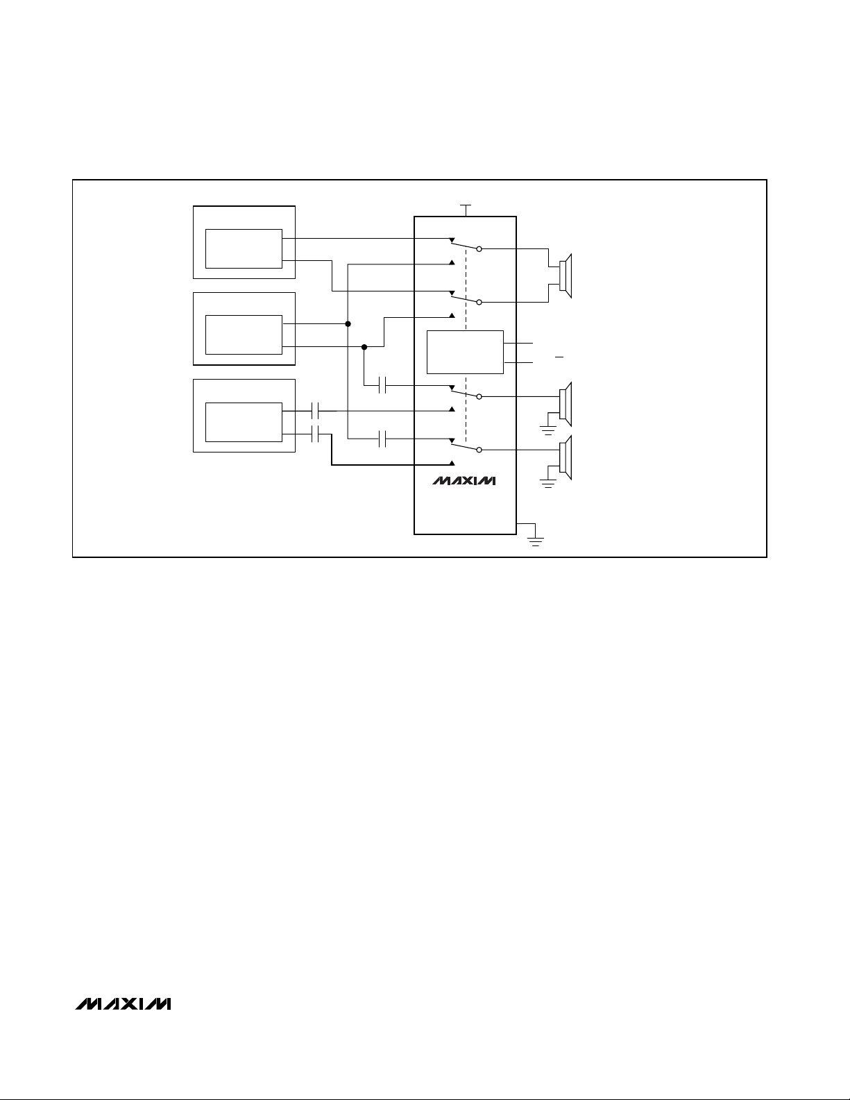
GND
V
CC
1.8V TO 5.5V
NO2
COM2
NC4
NO4
COM4
NC2
VOICE
AMP
MELODY IC
CODEC
CODEC
MP3
CB1 (CB)
DISCHARGE
CONTROL/
SIGNAL CONTROL
CB2 (EN)
NO1
COM1
NC3
NC1
NO3
COM3
SPEAKER 8Ω
MAX4910
MAX4911
MAX4912
( ) IS FOR MAX4911 ONLY
Figure 1. Typical Application Circuit
Page 10

MAX4910/MAX4911/MAX4912
Quad-SPDT, Clickless Audio Switches
with Negative Signal Handling
10 ______________________________________________________________________________________
tr < 5ns
tf < 5ns
50%
0V
LOGIC
INPUT
R
L
COM_
GND
CB_
C
L
INCLUDES FIXTURE AND STRAY CAPACITANCE.
V
NO_
V
CC
t
OFF
0V
NO_
OR NC_
0.8 x V
0UT
0.8 x V
OUT
t
ON
V
OUT
SWITCH
OUTPUT
LOGIC
INPUT
CB DEPENDS ON SWITCH CONFIGURATION;
INPUT POLARITY DETERMINED BY SENSE OF SWITCH.
V
CC
C
L
V
CC
V
OUT
MAX4910
MAX4911
MAX4912
Test Circuits/Timing Diagrams
Figure 2. Switching Time
50%
V
CC
0V
LOGIC
INPUT
V
OUT
0.8 x V
OUT
t
BBM
LOGIC
INPUT
R
L
GND
C
L
INCLUDES FIXTURE AND STRAY CAPACITANCE.
NO_
CB_
NC_
V
OUT
V
CC
V
CC
C
L
V
N_
COM_
MAX4910
MAX4911
MAX4912
Figure 3. Break-Before-Make Interval
V
GEN
GND
COM_
C
L
V
OUT
V
CC
V
OUT
CB_
OFF
ON
OFF
∆V
OUT
Q = (∆V
OUT
)(CL)
NC_
LOGIC INPUT WAVEFORMS INVERTED FOR SWITCHES
THAT HAVE THE OPPOSITE LOGIC SENSE.
OFF
ON
OFF
CB_
V
IL
TO V
IH
V
CC
R
GEN
CB_
OR NO_
MAX4910
MAX4911
MAX4912
Figure 4. Charge Injection
Page 11

MAX4910/MAX4911/MAX4912
Quad-SPDT, Clickless Audio Switches
with Negative Signal Handling
______________________________________________________________________________________ 11
MEASUREMENTS ARE STANDARDIZED AGAINST SHORTS AT IC TERMINALS.
OFF-ISOLATION IS MEASURED BETWEEN COM_ AND "OFF" NO_ OR NC_ TERMINAL ON EACH SWITCH.
ON-LOSS IS MEASURED BETWEEN COM_ AND "ON" NO_ OR NC_ TERMINAL ON EACH SWITCH.
CROSSTALK IS MEASURED FROM ONE CHANNEL TO THE OTHER CHANNEL.
SIGNAL DIRECTION THROUGH SWITCH IS REVERSED; WORST VALUES ARE RECORDED.
+5V
V
OUT
V
CC
CB_
NC_
COM_
NO_
V
IN
OFF-ISOLATION = 20log
V
OUT
V
IN
ON-LOSS = 20log
V
OUT
V
IN
CROSSTALK = 20log
V
OUT
V
IN
NETWORK
ANALYZER
50Ω
50Ω 50Ω
50Ω
MEAS REF
10nF
0V OR V
CC
50Ω
GND
MAX4910
MAX4911
MAX4912
Test Circuits/Timing Diagrams (continued)
Figure 5. On-Loss, Off-Isolation, and Crosstalk
CAPACITANCE
METER
NC_ or
NO_
COM_
GND
CB_
V
IL
OR V
IH
10nF
V
CC
f = 1MHz
V
CC
MAX4910
MAX4911
MAX4912
Figure 6. Channel Off-/On-Capacitance
Page 12

MAX4910/MAX4911/MAX4912
Quad-SPDT, Clickless Audio Switches
with Negative Signal Handling
12 ______________________________________________________________________________________
GND
V
CC
1.8V TO 5.5V
NO2
COM2
NC4
NO4
COM4
NC2
VOICE
AMP
MELODY IC
UART
CODEC
CB1 (CB)
DISCHARGE
CONTROL/
SIGNAL CONTROL
CB2 (EN)
NO1
COM1
NC3
NC1
NO3
COM3
SPEAKER 8Ω
MAX4910
MAX4911
MAX4912
( ) IS FOR MAX4911 ONLY.
HEADPHONES OR UART
Typical Operating Circuit
Chip Information
PROCESS: BiCMOS
Page 13

MAX4910/MAX4911/MAX4912
Quad-SPDT, Clickless Audio Switches
with Negative Signal Handling
Maxim cannot assume responsibility for use of any circuitry other than circuitry entirely embodied in a Maxim product. No circuit patent licenses are
implied. Maxim reserves the right to change the circuitry and specifications without notice at any time.
Maxim Integrated Products, 120 San Gabriel Drive, Sunnyvale, CA 94086 408-737-7600 ____________________ 13
© 2006 Maxim Integrated Products Printed USA is a registered trademark of Maxim Integrated Products, Inc.
12x16L QFN THIN.EPS
0.10 C 0.08 C
0.10 M C A B
D
D/2
E/2
E
A1
A2
A
E2
E2/2
L
k
e
(ND - 1) X e
(NE - 1) X e
D2
D2/2
b
L
e
L
C
L
e
C
L
L
C
L
C
PACKAGE OUTLINE
21-0136
2
1
G
8, 12, 16L THIN QFN, 3x3x0.8mm
MARKING
AAAA
EXPOSED PAD VARIATIONS
1.10
T1633-1
0.95
CODES
PKG.
T1233-1
MIN.
0.95
NOM.
1.10
D2
1.25
1.10
0.95
1.25
NOM.
1.10
MAX.
1.25
MIN.
0.95
MAX.
1.25
E2
12
N
k
A2
0.25
NE
A1
ND
0
0.20 REF
-
-
3
0.0230.05
L
e
E
0.45
2.90
b
D
A
0.20
2.90
0.70
0.50 BSC.
0.55
3.00
0.65
3.10
0.25
3.00
0.75
0.30
3.10
0.80
16
0.20 REF
0.25
-
0
4
0.02
4
-
0.05
0.50 BSC.
0.30
2.90
0.40
3.00
0.20
2.90
0.70
0.25
3.00
0.75
3.10
0.50
0.80
3.10
0.30
PKG
REF. MIN.
12L 3x3
NOM. MAX. NOM.
16L 3x3
MIN. MAX.
0.35 x 45°
PIN ID
JEDEC
WEED-1
0.35 x 45° WEED-2
T1233-3
1.10
1.25
0.95 1.10
0.35 x 45°1.25 WEED-1
0.95
T1633F-3
0.65
T1633-4
0.95
0.80
0.95
0.65
0.80
1.10
1.25
0.95
1.10
0.225 x 45°
0.95
WEED-2
0.35 x 45°
1.25
WEED-2
T1633-2
0.95
1.10
1.25
0.95
1.10
0.35 x 45°
1.25
WEED-2
NO
DOWN
BONDS
ALLOWED
YES
NO
YES
N/A
NO
PACKAGE OUTLINE
21-0136
2
2
G
8, 12, 16L THIN QFN, 3x3x0.8mm
YESWEED-11.25
1.100.95
0.35 x 45°
1.25
1.10
0.95
T1233-4
T1633FH-3
0.65
0.80
0.95
0.225 x 45°
0.65
0.80
0.95
WEED-2
N/A
NOTES:
1. DIMENSIONING & TOLERANCING CONFORM TO ASME Y14.5M-1994.
2. ALL DIMENSIONS ARE IN MILLIMETERS. ANGLES ARE IN DEGREES.
3. N IS THE TOTAL NUMBER OF TERMINALS.
4. THE TERMINAL #1 IDENTIFIER AND TERMINAL NUMBERING CONVENTION SHALL CONFORM TO
JESD 95-1 SPP-012. DETAILS OF TERMINAL #1 IDENTIFIER ARE OPTIONAL, BUT MUST BE LOCATED
WITHIN THE ZONE INDICATED. THE TERMINAL #1 IDENTIFIER MAY BE EITHER A MOLD OR
MARKED FEATURE.
5. DIMENSION b APPLIES TO METALLIZED TERMINAL AND IS MEASURED BETWEEN 0.20 mm AND 0.25 mm
FROM TERMINAL TIP.
6. ND AND NE REFER TO THE NUMBER OF TERMINALS ON EACH D AND E SIDE RESPECTIVELY.
7. DEPOPULATION IS POSSIBLE IN A SYMMETRICAL FASHION.
8. COPLANARITY APPLIES TO THE EXPOSED HEAT SINK SLUG AS WELL AS THE TERMINALS.
9. DRAWING CONFORMS TO JEDEC MO220 REVISION C.
10. MARKING IS FOR PACKAGE ORIENTATION REFERENCE ONLY.
11. NUMBER OF LEADS SHOWN ARE FOR REFERENCE ONLY.
0.25 0.30 0.35
2
0.25
0
0.20 REF
--
0.02
0.05
0.35
8
2
0.55 0.75
2.90
2.90 3.00 3.10
0.65 BSC.
3.00 3.10
8L 3x3
MIN.
0.70 0.75 0.80
NOM. MAX.
TQ833-1
1.25
0.25
0.70
0.35 x 45° NOWEEC
1.25
0.70
0.25
Package Information
(The package drawing(s) in this data sheet may not reflect the most current specifications. For the latest package outline information,
go to www.maxim-ic.com/packages
.)
Boblet
 Loading...