

Page 1
General Description
The MAX4895E integrates level-translating buffers and
features R, G, B port protection for VGA signals.
The MAX4895E has H, V (horizontal, vertical) translating buffers that take low-level CMOS inputs from the
graphics outputs to meet full +5.0V, TTL-compatible
outputs. Each output can drive ±10mA and meet the
VESA®specification. In addition, the device takes the
+5.0V, direct digital control (DDC) signals and translates them to the lower level required by the graphics
device. This level is set by the user by connecting V
L
to
the graphics output supply. The R, G, B terminals protect the graphics output pins against electrostatic discharge (ESD) events. All seven outputs have high-level
ESD protection.
The MAX4895E is specified over the extended -40°C to
+85°C temperature range, and is available in a 16-pin,
3mm x 3mm TQFN package.
Applications
Notebook Computers
Desktops
Servers
Graphics Cards
Features
♦ ESD Protection on H1, V1, SDA1, SCL1, R, G, and B
±15kV—Human Body Model
±8kV—IEC 61000-4-2, Contact Discharge
♦ Low Quiescent Current, IQ≤ 5µA (max)
♦ Low 3pF (max) Capacitance (R, G, B Ports)
♦ DDC Level-Shifting Protection and Isolation
♦ Horizontal Sync, Vertical Sync Level Shifting/
Buffering
♦ Input Compatible with V
L
♦ Output Full +5.0V TTL Compatible (per VESA)
♦ ±10mA Drive on Each H, V Terminal
♦ Space-Saving, Lead-Free, 16-Pin (3mm x 3mm)
TQFN Package
MAX4895E
VGA Port Protector
________________________________________________________________
Maxim Integrated Products
1
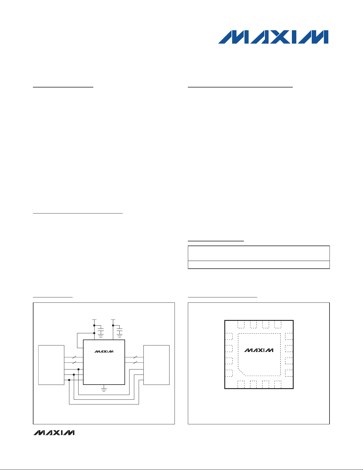
Pin Configuration
Ordering Information
Typical Operating Circuit
19-4569; Rev 0; 4/09
For pricing, delivery, and ordering information, please contact Maxim Direct at 1-888-629-4642,
or visit Maxim’s website at www.maxim-ic.com.
PART TEMP RANGE
PIN-
PACKAGE
TOP
MARK
MAX4895EETE+ -40°C to +85°C 16 TQFN-EP* AHEEAA
+
Denotes a lead(Pb)-free/RoHS-compliant package.
*
EP = Exposed pad.
VESA is a registered trademark of Video Electronics Standards
Association Corporation.
L
MAX4895E
GND
1μF
+5V
V
CC
H1, V1
SDA1, SCL1
N.C.
1μF
2
2
+3.3V
V
VGA OUTPUTS VGA PORT
EN
2
H0, V0
2
SDA0, SCL0
R
G
B
TOP VIEW
H1
12 10 9
13
V0
14
V1
15
V
CC
16
EN
+
13
R
(3mm × 3mm)
*CONNECT EXPOSED PAD TO GND.
MAX4895E
SCL1
SCL0
11
8
7
6
*EP
5
2
GH0
4
B
GND
TQFN
SDA1
SDA0
N.C.
V
L
Page 2
MAX4895E
VGA Port Protector
2 _______________________________________________________________________________________
ABSOLUTE MAXIMUM RATINGS
ELECTRICAL CHARACTERISTICS
(V
CC
= +4.5V to +5.5V, VL= +2.0V to VCC, TA= T
MIN
to T
MAX
, unless otherwise noted. Typical values are at VCC= +5.0V,
V
L
= +3.3V, and TA= +25°C.) (Note 2)
Stresses beyond those listed under “Absolute Maximum Ratings” may cause permanent damage to the device. These are stress ratings only, and functional
operation of the device at these or any other conditions beyond those indicated in the operational sections of the specifications is not implied. Exposure to
absolute maximum rating conditions for extended periods may affect device reliability.
Note 1: Package thermal resistances were obtained using the method described in JEDEC specification JESD51-7, using a four-
layer board. For detailed information on package thermal considerations, refer to www.maxim-ic.com/thermal-tutorial
.
(All voltages referenced to GND.)
V
CC
........................................................................-0.3V to +6.0V
V
L
.............................................................-0.3V to +(VCC+ 0.3V)
R, G, B, H1, V1, SCL1, SDA1...................-0.3V to +(V
CC
+ 0.3V)
EN, H0, V0, SCL0, SDA0 ............................-0.3V to +(V
L
+ 0.3V)
Continuous Current through SDA_, SCL_.........................±30mA
Continuous Short-Circuit Current H1, V1..........................±20mA
Continuous Power Dissipation (T
A
= +70°C) for multilayer
board:
16-Pin TQFN (derate 20.8mW/°C above +70°C) .......1667mW
Junction-to-Case Thermal Resistance (θ
JC
) (Note 1) ......7°C/W
Junction-to-Ambient Thermal Resistance (θ
JA
)
(Note 1) ........................................................................48°C/W
Operating Temperature Range ...........................-40°C to +85°C
Junction Temperature......................................................+150°C
Storage Temperature Range .............................-65°C to +150°C
Lead Temperature (soldering, 10s) .................................+300°C
PARAMETER SYMBOL CONDITIONS MIN TYP MAX UNITS
SUPPLY OPERATION
Supply Voltage VCC 4.5 5.5 V
Logic Supply Voltage VL VL VCC 2 3.3 5.5 V
VCC Supply C urrent ICC VH0, VV0 = 0, VEN = VL 0.5 5.0 μA
VL Supply C urrent IL VH0, VV0 = 0, VEN = VL (no load) 0.5 5.0 μA
RGB CHANNELS
R, G, B Capacitance C
f = 1MHz, V
OUT
R, G, B Leakage VCC = +5.5V -1 +1 μA
H_, V_, EN CHANNELS
Input Threshold Low VIL VL = +3.0V 0.8 V
Input Threshold High VIH VL = +3.6V 2.0 V
Input Hystere sis V
Input Leakage Current I
Output-Voltage Low VOL I
Output-Voltage High VOH I
Propagat ion Delay t
Enable Time tON, t
100 mV
HYST
VL = +3.3V, VCC = +5.5V -1 +1 μA
LEAK
OUT
OUT
PD
RL = 2.2k, CL = 10pF, VOL = +0.8V,
V
15 ns
OFF
SDA_, SCL_ (DDC) CHANNELS
On-Resistance, SDA, SCL R
Leakage Current, SDA, SCL I
ON
LEAK
VCC = +5.5V, I
V
VL = 0 -1 +1 μA
R,G,B
= 1V
(Note 3) 2.2 pF
P-P
= 10mA sink, VCC = +4.5V 0.8 V
= 10mA source, VCC = +4.5V 2.4 V
= +2.4V
OH
= ±10mA,
SDA, SCL
SDA SCL
= +0.5V
15 ns
20 55
Page 3
MAX4895E
VGA Port Protector
_______________________________________________________________________________________ 3
ELECTRICAL CHARACTERISTICS (continued)
(V
CC
= +4.5V to +5.5V, VL= +2.0V to VCC, TA= T
MIN
to T
MAX
, unless otherwise noted. Typical values are at VCC= +5.0V,
V
L
= +3.3V, and TA= +25°C.) (Note 2)
Note 2: All devices are 100% production tested at TA= +25°C. All temperature limits are guaranteed by design.
Note 3: Guaranteed by design, not production tested.
Note 4: Tested terminals to GND; 1µF bypass capacitors on V
CC
and VL.
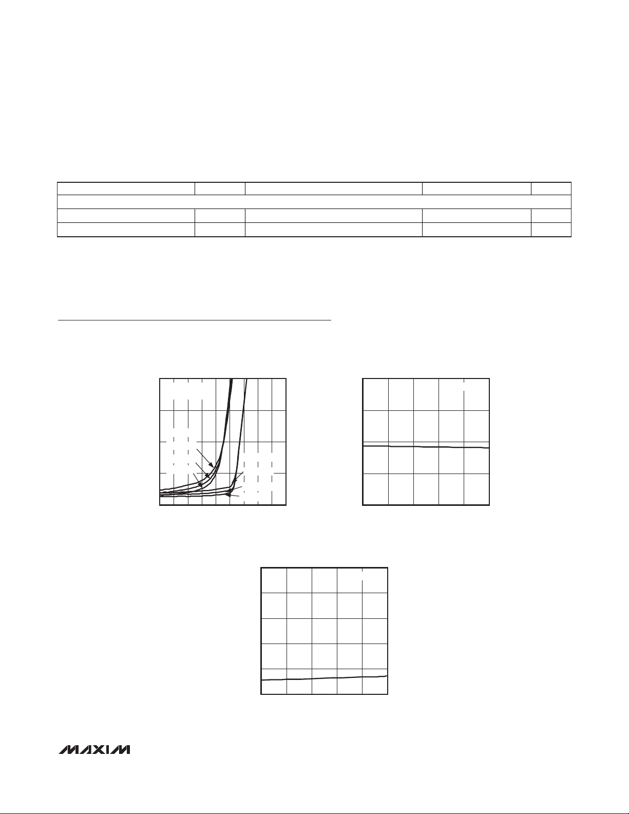
Typical Operating Characteristics
(VCC= +5.0V, VL= +3.3V, and TA= +25°C, unless otherwise noted.)
PARAMETER SYMBOL CONDITIONS MIN TYP MAX UNITS
ESD PROTECTION
SDA1, SCL1, H1, V1, R, G, B Human Body Model (Note 4) ±15 kV
SDA1, SCL1, H1, V1, R, G, B IEC 61000-4-2 Contact ±8 kV
60
RON vs. V
SDA0, SCL0 ARE
INTERCHANGEABLE
45
VCL = +3.3V
(Ω)
30
ON
TA = +85°C
R
TA = +25°C
TA = -40°C
15
0
0 4.5
SDA0
TA = -40°C
2.01.51.0 3.02.5 4.00.5 3.5
V
(V)
SDA0
VCL = +5V
TA = +85°C
TA = +25°C
MAX4895E toc01
OUTPUT VOLTAGE (V)
HV BUFFER OUTPUT-VOLTAGE
HIGH vs. TEMPERATURE
6.0
5.5
5.0
4.5
4.0
-40 85
10-15 35 60
TEMPERATURE (°C)
I
= 8mA
OUT
MAX4895E toc02
HV BUFFER OUTPUT-VOLTAGE
LOW vs. TEMPERATURE
1.0
0.8
0.6
0.4
OUTPUT VOLTAGE (V)
0.2
0
-40 85
10-15 35 60
TEMPERATURE (°C)
I
= 8mA
OUT
MAX4895E toc03
Page 4

MAX4895E
Applications Information
The MAX4895E provides the level shifting necessary to
drive two standard VGA ports from a graphics controller
as low as +2.2V. Internal buffers drive the HSYNC and
VSYNC signals to VGA standard TTL levels. The DDC
switch provides level shifting by clamping signals to a
diode drop less than VL(see the
Typical Operating
Circuit
). Connect VLto +3.3V for normal operation.
Power-Supply Decoupling
Bypass VCCand VLto ground with a 1µF ceramic
capacitor as close as possible to the device.
PCB Layout
High-speed switches such as the MAX4895E require
proper PCB layout for optimum performance. Ensure
that impedance-controlled PCB traces for high-speed
signals are matched in length and are as short as possible. Connect the exposed pad to a solid ground
plane.
Detailed Description
The MAX4895E integrates level-translating buffers and
features R, G, B port protection for VGA signals.
Horizontal and vertical synchronization (H0/V0) inputs
feature level-shifting buffers to support low-voltage
CMOS or standard TTL-compatible graphics controllers. The device meets ±10µA VESA drive requirements. The MAX4895E also features I2C level shifting
using two nMOS devices. All outputs maintain ±15kV
Human Body Model (HBM) and ±8kV Contact
Discharge per IEC 61000-4-2 on seven terminals
(SDA1, SCL1, H1, V1, R, G, B). The R, G, B pads protect the digital-to-analog converter (DAC) and are simply placed in parallel with the R, G, B outputs for the
DAC and VGA socket.
VGA Port Protector
4 _______________________________________________________________________________________
Pin Description
PIN NAME FUNCTION
1 R High-ESD Protection Diode s for RGB Signal s
2 G High-ESD Protection Diodes for RGB Signal s
3 B High-ESD Protection Diode s for RGB Signal s
4 GND Ground
5 VL Supply Voltage, +2.0V to VCC. Bypa ss VL to GND with a 1μF ceramic capacitor.
6 N.C. No Connection. Leave unconnected.
7 SDA0 SDA I/O. SDA0 referenced to VL.
8 SDA1 SDA I/O. SDA1 referenced to VCC.
9 SCL0 SCL I/O. SCL0 referenced to VL.
10 SCL1 SCL I/O. SCL1 referenced to VCC.
11 H0 Horizontal Sync Input
12 H1 Horizontal Sync Output
13 V0 Vertical Sync Input
14 V1 Vertical Sync Output
15 VCC Power-Supply Voltage, +4.5V to +5.5V. Bypass VCC to GND with a 1μF ceramic capacitor.
16 EN Enable for H1 and V1 Outputs
— EP
Exposed Pad. Connect EP to GND or leave unconnected. For enhanced thermal dissipation,
connect EP to a copper area a s large as possible. Do not use EP as a sole ground connection.
Page 5

MAX4895E
VGA Port Protector
_______________________________________________________________________________________ 5
Functional Diagram
SDA0
SCL0
V
L
CLAMP
H0
EN
V0
V
CC
SDA1
±15kV±15kV
SCL1
H1
±15kV±15kV±15kV
V1
R
G
B
MAX4895E
±15kV
±15kV
GND
Page 6

MAX4895E
VGA Port Protector
6 _______________________________________________________________________________________
Horizontal/Vertical Sync Level Shifter
HSYNC/VSYNC are buffered to provide level shifting
and drive capability to meet the VESA specification.
Input logic levels (VIL, VIH) are connected to VL(see
the
Electrical Characteristics
table). The level-shifted
outputs (H1 and V1) are pulled low when EN is driven
low (see Table 1). Logic-level output (V
OL
, VOH) are
+5.0V TTL compatible.
Display Data Channel Switches
The MAX4895E incorporates two nMOS switches for I2C
level shifting. The SDA, SCL terminals are voltage
clamped to a diode drop less than the VLvoltage.
Voltage clamping provides protection and compatibility
with SDA, SCL signals and low-voltage ASICs. Supply
+2.5V to +3.3V on VLto provide voltage clamping for
VESA I2C-compatible signals. The SDA, SCL switches
are identical, and each switch can be used to route
SDA or SCL signals.
RGB
There are three terminals for R, G, and B. The only
function of these terminals is to provide high-level ESD
protection to the RGB lines, while at the same time,
keeping the capacitance on the RGB lines to a minimum. The R, G, B terminals are identical, and any of
the three terminals can be used to protect red, green,
or blue video signals.
ESD Protection
As with all Maxim devices, ESD-protection structures
are incorporated on all terminals to protect against
electrostatic discharges encountered during handling
and assembly. Additionally, the MAX4895E is protected
to ±15kV on the RGB terminals and outputs H1, V1,
SDA1, and SCL1 by the Human Body Model (HBM). For
optimum ESD performance, bypass VCCto ground with
a 1µF ceramic capacitor.
ESD protection can be tested in various ways. The R,
G, B terminals and outputs H1, V1, SDA1, and SCL1 of
the MAX4895E are characterized for protection to the
following limits:
• ±15kV using the Human Body Model
• ±8kV IEC 61000-4-2 Contact Discharge
ESD Test Conditions
ESD performance depends on a variety of conditions.
Contact Maxim for a reliability report documenting test
setup, methodology, and results.
Table 1. HV Truth Table
Table 2. DDC Truth Table
EN FUNCTION
1 HSYNC/VSYNC level shifting enabled
0 H1, V1 = 0
EN FUNCTION
1
0 SDA1, SCL1, high impedance
SDA0 to SDA1
SCL0 to SCL1
Page 7

Human Body Model (HBM)
Figure 1a shows the Human Body Model, and Figure
1b shows the current waveform it generates when discharged into a low impedance. This model consists of a
100pF capacitor charged to the ESD voltage of interest
that is then discharged into the test device through a
1.5kΩ resistor.
IEC 61000-4-2
The IEC 61000-4-2 standard covers ESD testing and
performance of finished equipment. However, it does
not specifically refer to integrated circuits. The
MAX4895E assists in designing equipment to meet IEC
61000-4-2 without the need for additional ESD-protection components.
The major difference between tests done using the
Human Body Model and IEC 61000-4-2 is higher peak
current in IEC 61000-4-2 because series resistance is
lower in the IEC 61000-4-2 model. Hence, the ESD withstand voltage measured to IEC 61000-4-2 is generally
lower than that measured using the Human Body Model.
Figure 1c shows the IEC 61000-4-2 model, and Figure
1d shows the current waveform for IEC 61000-4-2 ESD
Contact Discharge test.
Chip Information
PROCESS: BiCMOS
MAX4895E
VGA Port Protector
_______________________________________________________________________________________ 7
Figure 1a. Human Body ESD Test Model
Figure 1b. Human Body Current Waveform
Figure 1c. IEC 61000-4-2 ESD Test Model
Figure 1d. IEC 61000-4-2 ESD Generator Current Waveform
HIGH-
VOLTAGE
DC
SOURCE
R
C
1MΩ
CHARGE-CURRENT-
LIMIT RESISTOR
C
s
100pF
R
D
1500Ω
DISCHARGE
RESISTANCE
STORAGE
CAPACITOR
DEVICE
UNDER
TEST
HIGH-
VOLTAGE
DC
SOURCE
R
C
50MΩ TO 100MΩ
CHARGE-CURRENT-
LIMIT RESISTOR
C
s
150pF
R
D
330Ω
DISCHARGE
RESISTANCE
STORAGE
CAPACITOR
DEVICE
UNDER
TEST
AMPS
IP 100%
90%
36.8%
10%
0
0
t
RL
CURRENT WAVEFORM
TIME
I
r
t
DL
PEAK-TO-PEAK RINGING
(NOT DRAWN TO SCALE)
I
100%
90%
PEAK
I
10%
tr = 0.7ns TO 1ns
30ns
60ns
t
Page 8

MAX4895E
VGA Port Protector
Maxim cannot assume responsibility for use of any circuitry other than circuitry entirely embodied in a Maxim product. No circuit patent licenses are
implied. Maxim reserves the right to change the circuitry and specifications without notice at any time.
8
_____________________Maxim Integrated Products, 120 San Gabriel Drive, Sunnyvale, CA 94086 408-737-7600
© 2009 Maxim Integrated Products Maxim is a registered trademark of Maxim Integrated Products, Inc.
PACKAGE TYPE PACKAGE CODE DOCUMENT NO.
16 TQFN-EP T1633+4
21-0136
Package Information
For the latest package outline information and land patterns, go to www.maxim-ic.com/packages.
 Loading...