

Page 1

19-4269; Rev 0; 10/08
EVALUATION KIT
AVAILABLE
Ultra-Low Capacitance 1:2 VGA
Switch with ±15kV ESD
General Description
The MAX4885E integrates high-bandwidth analog
switches and level-translating buffers to implement a
complete 1:2 multiplexer for VGA signals. The device
provides switching for RGB, display data channel (DDC).
Horizontal and vertical synchronization (HSYNC/VSYNC)
inputs feature level-shifting buffers to support low-voltage CMOS or standard TTL-compatible graphics controllers, meeting the VESA requirement of ±8mA. DDC,
consisting of SDA_ and SCL_, is a bidirectional activelevel translating switch that reduces capacitive load. The
MAX4885E features high ESD protection to ±15kV
Human Body Model (HBM) on all twelve externally routed terminals. See the
Pin Description
section. All other
pins are protected to ±10kV Human Body Model (HBM).
The MAX4885E is specified over the extended -40°C to
+85°C temperature range, and is available in the
24-pin, 4mm x 4mm TQFN package.
Applications
Notebook Computers/Docking Stations
Digital Projectors
Computer Monitors
Servers/Storage
KVM Switches
Features
♦ ±15kV HBM ESD Protection on Externally Routed
Terminals
♦ 1GHz Bandwidth
♦ Low 5Ω (typ) On-Resistance (R, G, B Signals)
♦ Low 6pF (typ) On-Capacitance (R, G, B Signals)
♦ Low R, G, B Skew -50ps (typ)
♦ Near Zero Power Consumption (< 2µA)
♦ Ultra-Small, 24-Pin (4mm x 4mm) TQFN Package
Ordering Information
PART TEMP RANGE PIN-PACKAGE
MAX4885EETG+ -40°C to +85°C 24 TQFN-EP*
*
EP = Exposed pad.
+
Denotes lead-free package/RoHS-compliant package.
MAX4885E
Pin Configuration
Typical Operating Circuit
TOP VIEW
G1
MAX4885E
R0
G2
B1
B2
12
V1
11
H1
10
GND
V
9
L
V
8
CC
V0
7
B0
G0
H0
+3.3V
0.1µF 0.1µF
3
GRAPHICS
CONTROLLER
DOCKING
STATION
2
2
+3.3V
V
L
R0, B0, G0
H0, V0
SDA0, SCL0
EN
SEL
+5.0V
V
MAX4885E
R1, G1, B1
SDA1, SCL1
R2, G2, B2
SDA2, SCL2
GND
CC
H1, V1
3
2
VGA
PORT
2
2
DOCKING
3
STATION
2
SCL2
SCL1
SDA2
SDA1
SEL
R1
R2
18 17 16 15 14 13
19
20
21
22
EN
23
*EP
24
+
12 3456
SCL0
SDA0
TQFN-EP
*EXPOSED PAD. CONNECTED TO GROUND OR LEAVE UNCONNECTED.
________________________________________________________________
Maxim Integrated Products
1
For pricing, delivery, and ordering information, please contact Maxim Direct at 1-888-629-4642,
or visit Maxim's website at www.maxim-ic.com.
Page 2
MAX4885E
Ultra-Low Capacitance 1:2 VGA
Switch with ±15kV ESD
2 _______________________________________________________________________________________
ABSOLUTE MAXIMUM RATINGS
Stresses beyond those listed under “Absolute Maximum Ratings” may cause permanent damage to the device. These are stress ratings only, and functional
operation of the device at these or any other conditions beyond those indicated in the operational sections of the specifications is not implied. Exposure to
absolute maximum rating conditions for extended periods may affect device reliability.
(All voltages referenced to GND.)
V
CC
, VL.....................................................................-0.3V to +6V
R_, G_, B_, SDA1, SCL1, SDA2, SCL2,
H1, V1, (Note 1) ........................................-0.3V to V
CC
+ 0.3V
H0, V0, SDA0, SCL0, EN, SEL.........................-0.3V to V
L
+ 0.3V
Continuous Current through RGB Switches .....................±30mA
Continuous Current through DDC Switches .....................±30mA
Peak Current through RGB Switches
(pulsed at 1ms, 10% duty cycle)...................................±90mA
Peak Current through DDC Switches (pulsed at 1ms,
10% duty cycle)............................................................±90mA
Continuous Power Dissipation (T
A
= +70°C)
24-Pin TQFN (derate 27.8mW/°C above +70°C) ........2222mW
Junction to Ambient Thermal Resistance (θ
JA
) (Note 2)
24-Pin TQFN..................................................................36°C/W
Junction to Ambient Thermal Resistance (θ
JC
) (Note 2)
24-Pin TQFN....................................................................3°C/W
Operating Temperature Range ...........................-40°C to +85°C
Storage Temperature Range .............................-65°C to +150°C
Junction Temperature......................................................+150°C
Lead Temperature (soldering, 10s) .................................+300°C
ELECTRICAL CHARACTERISTICS
(VCC= +5.0V ±10%, VL= +2V to +5.5V, TA= T
MIN
to T
MAX
, unless otherwise noted. Typical values are at VCC= +5.0V, VL= +3.3V and
T
A
= +25°C.) (Note 3)
PARAMETER
CONDITIONS
EN = V
L
VCC Quiescent Supply Current I
CC
VCC = +5.0V
EN = GND
1µA
EN = V
L
VL Quiescent Supply Current I
VL
VL = +3.3V
EN = GND
1µA
RGB ANALOG SWITCHES
On-Resistance R
ON
VCC = +5.0V, IIN = -10mA, VIN = +0.7V
(Note 4)
6 Ω
On-Resistance Matching ΔR
ON
0 ≤ VIN ≤ 0.7V, IIN = -10mA 0.5 Ω
On-Resistance Flatness
)
0 ≤ VIN ≤ 0.7V, IIN = -10mA 0.5 Ω
Off-Leakage Current I
L(OFF)
VCC = +5.5V, VIN = +0.3V or +5.5V,
V
EN
= 0 or V
L
-1 +1 µA
On-Leakage Current I
L(ON)
VCC = +5.5V, VIN = +0.3V or +5.5V,
V
EN
= V
L
-1 +1 µA
HV BUFFER
Input Voltage Low V
ILHV
0.33 x
V
L
V
Input Voltage High V
IHHV
0.66 x
V
L
V
Input Logic Hysteresis V
HYST
75 mV
Input Leakage Current I
INHV
VCC = +5.5V, VL = +5.5V, V
IN
= 0 or V
L
-1 +1 µA
High-Output Drive Current I
OHHV
V
OHHV
≥ 3.0V 8.0 mA
Low-Output Drive Current I
OLHV
V
OLHV
≤ 0.6V 8.0 mA
Note 1: Signals exceeding VCCor GND are clamped by internal diodes. Limit forward-diode current to maximum current rating.
Note 2: Package thermal resistances were obtained using the method described in JEDEC specifications. For detailed information
on package thermal considerations, refer to www.maxim-ic.com/thermal-tutorial
.
SYMBOL
MIN TYP MAX UNITS
R
FLAT(ON
Page 3
MAX4885E
Ultra-Low Capacitance 1:2 VGA
Switch with ±15kV ESD
_______________________________________________________________________________________ 3
PARAMETER
SYMBOL
CONDITIONS
MIN
TYP
MAX
UNITS
SDA_, SCL_
Supply Voltage V
L
2.0 5.5 V
On-Resistance R
ON
VIN = +0.4V, IIN = ±2mA, VL = +2.0V 10 Ω
On-Capacitance C
ON
f = 100kHz 15 pF
High-Impedance Input Leakage
Current
I
INHIZ
EN = GND, V
CC
= +5.5V, VL = +3.6V,
SCL0, SDA0, SCL1, SCL2, SDA1, SDA2
= GND or V
VL
(Note 5)
-1 +1 µA
Off-Input Leakage Current I
INOFF
EN = VL, VL = +3.6V, V
IN
= VL - 0.2V -1 +1 µA
CONTROL LOGIC (SEL, EN)
Input Voltage Low V
ILLOG
0.33 x
V
L
V
Input Voltage High
0.66 x
V
L
V
Input Logic Hysteresis V
HYST
75 mV
Input Leakage Current I
INLEK
VCC = +5.5V, VL = +3.6V, V
IN
= 0 or V
L
-1 +1 µA
ESD PROTECTION
Human Body Model; R1, G1, B1, R2, G2,
B2, SDA1, SCL1, SDA2, SCL2, H1, V1
ESD Protection
Human Body Model; all other pins
kV
ELECTRICAL CHARACTERISTICS (continued)
(VCC= +5.0V ±10%, VL= +2V to +5.5V, TA= T
MIN
to T
MAX
, unless otherwise noted. Typical values are at VCC= +5.0V, VL= +3.3V and
T
A
= +25°C.) (Note 3)
PARAMETER
CONDITIONS
Bandwidth f
MAX
RS = RL = 50Ω 1GHz
Insertion Loss I
LOS
f = 1MHz, RS = RL = 50Ω, Figure 1 0.6 dB
Crosstalk V
CT
f = 50MHz, RS = RL = 50Ω, Figure 1 -40 dB
Off-Capacitance C
OFF
f = 250MHz 4.5 pF
On-Capacitance C
ON
f = 250MHz 6.4 pF
AC ELECTRICAL CHARACTERISTICS
(VCC= +5.0V ±10%, VL= +2V to +5.5V, TA= T
MIN
to T
MAX
, unless otherwise noted. Typical values are at VCC= +5.0V, VL= +3.3V and
T
A
= +25°C.) (Note 3)
V
IHLOG
±15
±10
SYMBOL
MIN TYP MAX UNITS
Page 4
MAX4885E
Ultra-Low Capacitance 1:2 VGA
Switch with ±15kV ESD
4 _______________________________________________________________________________________
PARAMETER
CONDITIONS
RGB ANALOG SWITCHES
Output Skew Between Ports t
SKEW
Skew between any two ports: R_, G_, B_,
Figure 2
50 ps
HV BUFFER
Propagation Delay t
PD
RL = 1kΩ, CL = 10pF, Figure 2 15 ns
TIMING CHARACTERISTICS
(VCC= +5.0V ±10%, VL= +2V to +5.5V, TA= T
MIN
to T
MAX
, unless otherwise noted. Typical values are at VCC= +5.0V, VL= +3.3V and
T
A
= +25°C.) (Note 3)
Note 3: All devices are 100% production tested at T
A
= +25°C. Specifications over the full temperature range are guaranteed by design.
Note 4: On-resistance guarantees the low-static logic level.
Note 5: SDA_, SCL_ off-input leakage current guarantees the high-static logic level.
RON vs. VR0*
(RGB SWITCHES)
MAX4885E toc01
V
R0
(V)
R
ON
(Ω)
0.80.60.40.2
1
2
3
4
5
6
7
8
9
10
0
010.70.50.30.1 0.9
TA = +85°C
T
A
= +25°C
TA = -40°C
*R0, G0, B0 ARE INTERCHANGEABLE
RON vs. V
SDA0
*
(DDC SWITCHES)
MAX4885E toc02
V
SDA0
(V)
R
ON
(Ω)
1.0 1.5 3.0 4.0
15
30
45
60
0
04.52.52.0 3.50.5
TA = +85°C
TA = +25°C
TA = -40°C
TA = +85°C
VL = +3.3V VL = +5.0V
TA = +25°C
TA = -40°C
SDA0, SCL0 ARE
INTERCHANGEABLE
HV BUFFER OUTPUT VOLTAGE
HIGH vs. TEMPERATURE
MAX4885E toc03
TEMPERATURE (°C)
OUTPUT VOLTAGE HIGH (V)
35
5
4
6
7
8
3
-40 85-15 6010
I
OUT
= 8mA
Typical Operating Characteristics
(VCC= +5.0V, VL= +3.3V and TA= +25°C, unless otherwise noted.)
SYMBOL
MIN TYP MAX UNITS
Page 5
MAX4885E
Ultra-Low Capacitance 1:2 VGA
Switch with ±15kV ESD
_______________________________________________________________________________________ 5
HV BUFFER OUTPUT VOLTAGE
LOW vs. TEMPERATURE
MAX4885E toc04
TEMPERATURE (°C)
OUTPUT VOLTAGE LOW (V)
35
0.4
0.2
0.6
0.8
1.0
0.0
-40 85-15 6010
I
OUT
= 8mA
SUPPLY CURRENT vs. TEMPERATURE
MAX4885E toc05
TEMPERATURE (°C)
SUPPLY CURRENT (μA)
35
0.2
0.1
0.3
0.4
0.5
0.0
-40 85-15 6010
I
CC
I
VL
Typical Operating Characteristics (continued)
(VCC= +5.0V, VL= +3.3V and TA= +25°C, unless otherwise noted.)
ON-RESPONSE vs. FREQUENCY
MAX4885E toc06
FREQUENCY (MHz)
ON-RESPONSE (dB)
10
-6
-8
-4
-2
0
-10
-5
-7
-3
-1
-9
1 1000100
CROSSTALK vs. FREQUENCY
MAX4885E toc07
FREQUENCY (MHz)
CROSSTALK (dB)
10
-60
-80
-40
-20
0
-100
-50
-70
-30
-10
-90
1 1000100
Page 6
MAX4885E
Ultra-Low Capacitance 1:2 VGA
Switch with ±15kV ESD
6 _______________________________________________________________________________________
Timing Circuits/Timing Diagrams
INPUT
OUTPUT
V
OH
t
PHL
t
PLH
t
SKEW
= |t
PLH
- t
PHL
|
t
PD
= MAX (t
PLH
, t
PHL
)
1V
50%
0
50%
0.9V
50%
50%
0
R
L
= 1kΩ
C
L
= 10pF
Figure 2. Propagation Delay and Skew Waveforms
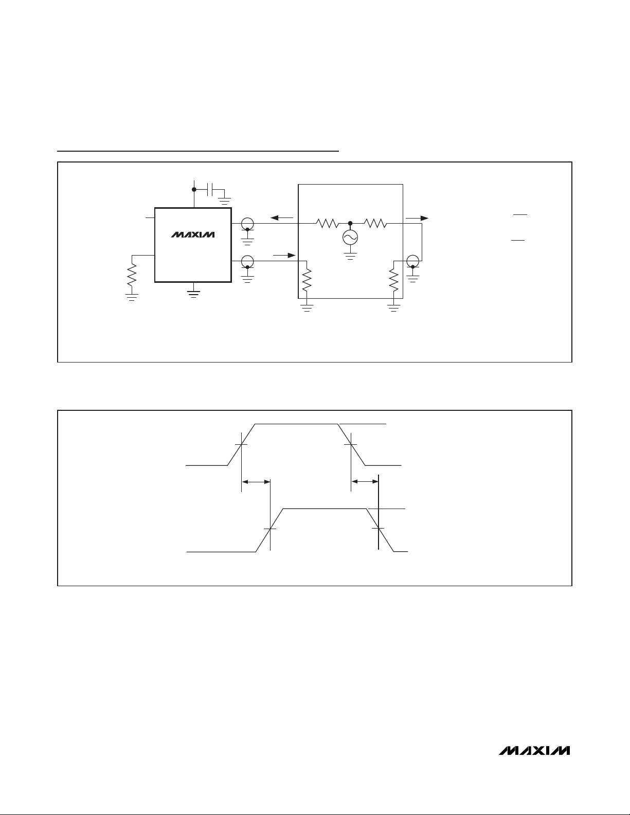
Figure 1. Insertion-Loss and Crosstalk
+5V
10nF
NETWORK
ANALYZER
0 OR V
50Ω
MEASUREMENTS ARE STANDARDIZED AGAINST SHORTS AT IC TERMINALS.
INSERTION-LOSS IS MEASURED BETWEEN R0 AND R1 OR R2 ON EACH SWITCH.
CROSSTALK IS MEASURED FROM ONE CHANNEL TO THE OTHER CHANNEL.
SIGNAL DIRECTION THROUGH SWITCH IS REVERSED; WORST VALUES ARE RECORDED.
SEL
CC
R1, G1, B1
V
CC
R0, G0, B0
MAX4885E
R2, G2, B2
GND
V
IN
V
OUT
50Ω
MEAS REF
50Ω 50Ω
50Ω
INSERTION-LOSS = 20log
CROSSTALK = 20log ✕
V
OUT
✕
V
IN
V
OUT
V
IN
Page 7
MAX4885E
Ultra-Low Capacitance 1:2 VGA
Switch with ±15kV ESD
_______________________________________________________________________________________ 7
Pin Description
PIN NAME FUNCTION
1 SDA0 SDA I/O
2 SCL0 SCL I/O
3 R0 RGB Analog I/O
4 G0 RGB Analog I/O
5 B0 RGB Analog I/O
6 H0 Horizontal Sync Input
7 V0 Vertical Sync Input
8VCCSupply Voltage. VCC = +5.0V ±10%. Bypass VCC to GND with a 0.1µF or larger ceramic capacitor.
9VLSupply Voltage. +2V ≤ VL ≤ +5.5V. Bypass VL to GND with a 0.1µF or larger ceramic capacitor.
10 GND Ground
11 H1 Horizontal Sync Output*
12 V1 Vertical Sync Output*
13 B2 RGB Analog I/O*
14 B1 RGB Analog I/O*
15 G2 RGB Analog I/O*
16 G1 RGB Analog I/O*
17 R2 RGB Analog I/O*
18 R1 RGB Analog I/O*
19 SCL2 SCL I/O*
20 SCL1 SCL I/O*
21 SDA2 SDA I/O*
22 SDA1 SDA I/O*
23 EN Enable Input. Drive EN high for normal operation. Drive EN low to disable the device.
24 SEL Select Input. Logic input for switching RGB and DDC swiches.
— EP Exposed Pad. Connect exposed pad to ground or leave unconnected.
Detailed Description
The MAX4885E integrates high-bandwidth analog
switches and level-translating buffers to implement a
complete 1:2 multiplexer for VGA signals. The device
provides switching for RGB, HSYNC, VSYNC, SDA_
and SCL_ signals.
The HSYNC and VSYNC inputs feature level-shifting
buffers to support TTL output logic levels from low-voltage graphics controllers. These buffered switches may
be driven from as little as +2.0V up to +5.5V. RGB signals are routed with the same high-performance analog
switches, and SDA_, SCL_ signals are voltage clamped
to a diode drop less than VL. Voltage clamping provides protection and compatibility with SDA_ and SCL_
signals and low-voltage ASICs. In keyboard/video/
mouse (KVM) applications, VLis normally set to +5V
because low-voltage clamping is not required, as specified by the VESA standard.
Drive EN logic-low to shut down the MAX4885E. In shutdown mode, all switches are high impedance, providing
high-signal rejection. The RGB, HSYNC, VSYNC, SDA_,
and SCL_ outputs are ESD protected to ±15kV by the
Human Body Model.
RGB Switches
The MAX4885E provides three SPDT high-bandwidth
switches to route standard VGA R, G, and B signals
(see Table 1). The R, G, and B analog switches are
identical, and any of the three switches can be used to
route red, green, or blue video signals.
*
Terminal as ±15kV ESD protection—Human Body Model.
Page 8

Horizontal/Vertical Sync Level Shifter
HSYNC/VSYNC are buffered to provide level shifting
and drive capability to meet the VESA specification.
Display-Data Channel Multiplexer
The MAX4885E provides two voltage-clamped switches
to route DDC signals (see Table 3). Each switch clamps
signals to a diode drop less than the voltage applied on
VL. Supply +3.3V on VLto provide voltage clamping for
VESA I2C-compatible signals. If voltage clamping is not
required, connect VLto VCC. The SDA_ and SCL_
switches are identical, and each switch can be used to
route either SDA_ and SCL_ signals.
ESD Protection
As with all Maxim devices, ESD-protection structures
are incorporated on all pins to protect against electrostatic discharges encountered during handling and
assembly. Additionally, the MAX4885E is protected to
±15kV on RGB, HSYNC, VSYNC, SDA_ and SCL_
outputs by the Human Body Model (HBM). See the
Pin
Description
section. For optimum ESD performance,
bypass each VCCpin to ground with a 0.1µF or larger
ceramic capacitor.
Human Body Model (HBM)
Several ESD testing standards exist for measuring the
robustness of ESD structures. The ESD protection of
the MAX4885E is characterized with the Human Body
Model. Figure 3 shows the model used to simulate an
ESD event resulting from contact with the human body.
The model consists of a 100pF storage capacitor that is
charged to a high voltage, then discharged through a
1.5kΩ resistor. Figure 4 shows the current waveform
when the storage capacitor is discharged into a low
impedance.
ESD Test Conditions
ESD performance depends on a variety of conditions.
Please contact Maxim for a reliability report documenting test setup, methodology, and results.
Applications Information
The MAX4885E provides the level shifting necessary to
drive two standard VGA ports from a graphics controller as low as +2.2V. Internal buffers drive the
HSYNC and VSYNC signals to VGA standard TTL levels. The DDC multiplexer provides level shifting by
clamping signals to a diode drop less than VL(see the
Typical Operating Circuit
). Connect VLto +3.3V for normal operation, or to VCCto disable voltage clamping for
DDC signals.
Power-Supply Decoupling
Bypass each VCCpin and VLto ground with a 0.1µF
or larger ceramic capacitor as close as possible to the
device.
PCB Layout
High-speed switches such as the MAX4885E require
proper PCB layout for optimum performance. Ensure
that impedance-controlled PCB traces for high-speed
signals are matched in length and as short as possible.
Connect the exposed pad to a solid ground plane.
Chip Information
PROCESS: BiCMOS
MAX4885E
Ultra-Low Capacitance 1:2 VGA
Switch with ±15kV ESD
8 _______________________________________________________________________________________
EN FUNCTION
0 H_, V_ = 0
Table 2. HV Truth Table
X = Don’t care.
EN SEL FUNCTION
10
SDA0 to SDA1
SCL0 to SCL1
11
SDA0 to SDA2
SCL0 to SCL2
0 X SDA_, SCL_, high impedance
Table 3. DDC Truth Table
X = Don’t care.
EN SEL FUNCTION
10
R0 to R1
G0 to G1
B0 to B1
11
R0 to R2
G0 to G2
B0 to B2
0 X R_, B_, and G_, high impedance
Table 1. RGB Truth Table
X = Don’t care.
Page 9
MAX4885E
Ultra-Low Capacitance 1:2 VGA
Switch with ±15kV ESD
_______________________________________________________________________________________ 9
Figure 3. Human Body ESD Test Model
Figure 4. HBM Discharge Current Waveform
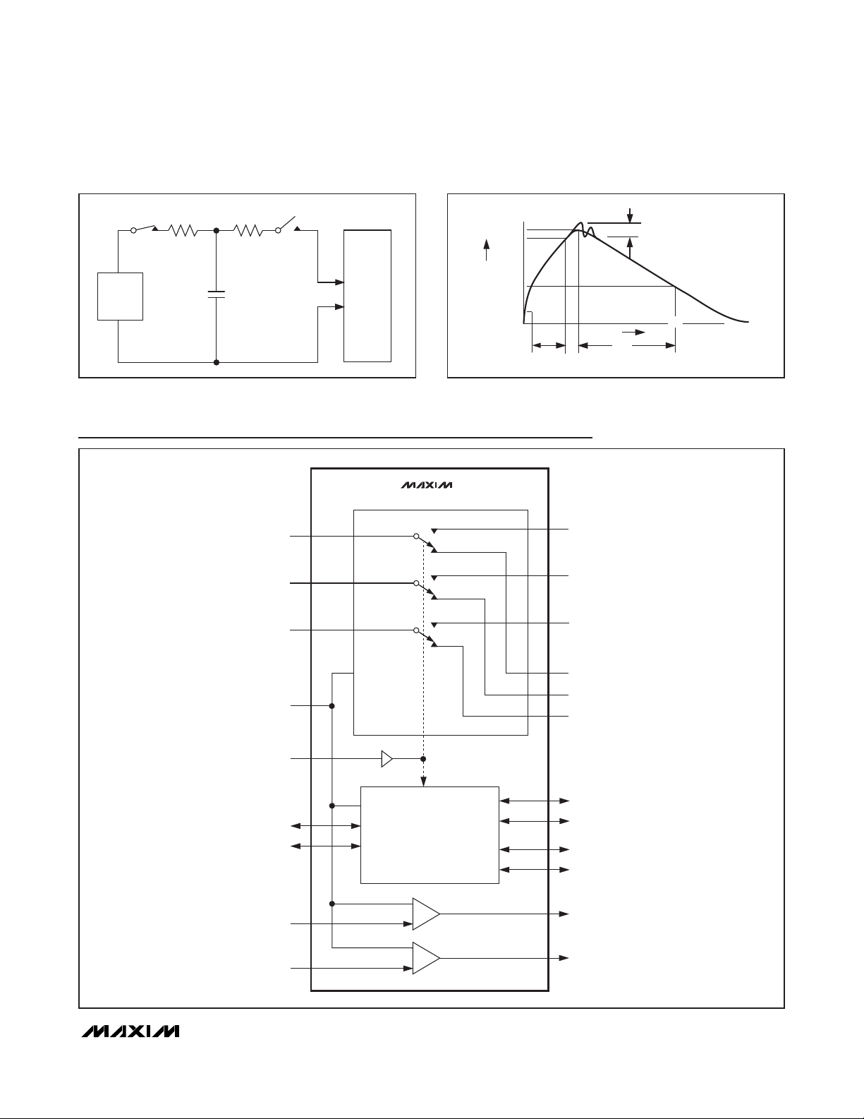
Functional Diagram
HIGH-
VOLTAGE
DC
SOURCE
R
C
1MΩ
CHARGE-CURRENT-
LIMIT RESISTOR
C
s
100pF
R
D
1500Ω
DISCHARGE
RESISTANCE
STORAGE
CAPACITOR
IP 100%
90%
AMPERES
DEVICE
UNDER
TEST
36.8%
10%
0
0
t
RL
TIME
t
DL
CURRENT WAVEFORM
MAX4885E
R0
G0
R1
G1
PEAK-TO-PEAK RINGING
I
R
(NOT DRAWN TO SCALE)
SEL
SDA0
SCL0
B0
EN
BIDIRECTIONAL
LEVEL SHIFTER
H0
V0
B1
R2
G2
B2
SDA1
SCL1
SDA2
SCL2
H1
V1
Page 10

MAX4885E
Ultra-Low Capacitance 1:2 VGA
Switch with ±15kV ESD
Maxim cannot assume responsibility for use of any circuitry other than circuitry entirely embodied in a Maxim product. No circuit patent licenses are
implied. Maxim reserves the right to change the circuitry and specifications without notice at any time.
10
____________________Maxim Integrated Products, 120 San Gabriel Drive, Sunnyvale, CA 94086 408-737-7600
© 2008 Maxim Integrated Products is a registered trademark of Maxim Integrated Products, Inc.
PACKAGE TYPE PACKAGE CODE DOCUMENT NO.
24 TQFN-EP T2444-4
21-0139
Package Information
For the latest package outline information and land patterns, go to www.maxim-ic.com/packages.
 Loading...