

Page 1

General Description
The MAX4885 integrates high-bandwidth analog
switches and level-translating buffers to implement a
complete 1:2 or 2:1 multiplexer for VGA signals. The
device provides switching for RGB, display data channel (DDC), and horizontal and vertical synchronization
(HSYNC, VSYNC) signals. A low-noise charge pump
with internal capacitors provides a boosted gate-drive
voltage to improve performance of the RGB switches.
In the 1:2 multiplexer mode, HSYNC/VSYNC inputs feature level-shifting buffers to support low-voltage CMOS
or standard TTL-compatible graphics controllers. In the
2:1 multiplexer mode, the output buffers for the
HSYNC/VSYNC inputs are disabled, allowing bidirectional signaling. In both modes, DDC signals are voltage-clamped to an external voltage to provide level
translation and protection. The MAX4885 features a
5µA shutdown mode and is ESD protected to ±8kV
Human Body Model (HBM) on externally routed pins.
The MAX4885 is specified over the extended (-40°C to
+85°C) temperature range, and is available in the 32pin, 5mm x 5mm TQFN package.
Applications
Notebook Computers
Digital Projectors
Computer Monitors
Servers
KVM Switches
Features
♦ +5V Single-Supply Operation
♦ Programmable Voltage Clamp for Open-Drain
DDC Signals
♦ Low 5Ω (typ) On-Resistance (R, G, B Signals)
♦ Low 13pF (typ) On-Capacitance (R, G, B Signals)
♦ Break-Before-Make Switching Protects Against
Circuit Shorts
♦ ±8kV HBM ESD Protection on Externally Routed
Pins
♦ Low 300µA Supply Current (Lower than 1µA with
Charge Pump Disabled)
♦ Space-Saving, Lead-Free, 32-Pin (5mm x 5mm)
TQFN Package
MAX4885
Complete VGA 1:2 or 2:1 Multiplexer
________________________________________________________________ Maxim Integrated Products 1
19-0554; Rev 0; 5/06
For pricing, delivery, and ordering information, please contact Maxim/Dallas Direct! at
1-888-629-4642, or visit Maxim’s website at www.maxim-ic.com.
MAX4885
TQFN
TOP VIEW
29
30
28
27
12
11
13
R0
B0
H0
V0
DDCA0
14
QP
H1
V+
GNDB1V2
H2
12
DDCA1
4567
2324 22 20 19 18
GND
V+
DDCB2
DDCA2
GND
V+
G0
V1
3
21
31
10
M
V
CL
32
9
SEL
EN
DDCB1
26
15
R2
R1
25
16
G2
DDCB0
B2
8
17
G1
*EXPOSED PADDLE CONNECTED TO GND
*EP
Pin Configuration
Ordering Information
GRAPHICS
CONTROLLER
V
CL
V+
GND
+3.3V
+5V
EN
SEL
R0, B0, G0
H0, V0
DDCA0, DDCB0
0.1µF
0.1µF
VGA
PORT 1
VGA
PORT 2
R2, G2, B2
H2, V2
DDCA2, DDCB2
2
3
2
2
3
2
R1, G1, B1
H1, V1
DDCA1, DDCB1
2
3
2
DOCKING
STATI ON
M
MAX4885
Typical Operating Circuit
PART
TEMP RANGE
PIN-PACKAGE
PKG
CODE
MAX4885ETJ+
32 TQFN-EP*
T3255-4
*EP = Exposed pad.
+Denotes lead-free package.
-40°C to +85°C
Page 2

MAX4885
Complete VGA 1:2 or 2:1 Multiplexer
2 _______________________________________________________________________________________
ABSOLUTE MAXIMUM RATINGS
Stresses beyond those listed under “Absolute Maximum Ratings” may cause permanent damage to the device. These are stress ratings only, and functional
operation of the device at these or any other conditions beyond those indicated in the operational sections of the specifications is not implied. Exposure to
absolute maximum rating conditions for extended periods may affect device reliability.
(All voltages referenced to GND.)
V
+
, VCL.....................................................................-0.3V to +6V
R_, G_, B_, DDCA_, DDCB_, SEL, M,
EN, QP (Note 1) ...........................................-0.3V to V+ + 0.3V
H_, V_ .......................................................................-0.3V to +6V
Continuous Current Through RGB Switches ....................±70mA
Continuous Current Through HV, DDC Switches…..........±50mA
Peak Current Through RGB Switches
(pulsed at 1ms, 10% duty cycle).................................±140mA
Peak Current Through HV, DDC Switches (pulsed at 1ms,
10% duty cycle)..............................................................±100mA
Continuous Power Dissipation (T
A
= +70°C)
32-Pin TQFN (derate 21.3mW/°C above +70°C) ........1702mW
Operating Temperature Range ...........................-40°C to +85°C
Storage Temperature Range .............................-65°C to +150°C
Junction Temperature......................................................+150°C
Lead Temperature (soldering, 10s) .................................+300°C
ELECTRICAL CHARACTERISTICS
(V+ = +5.0V ±10%, VCL= +3.3V ±10%, TA= T
MIN
to T
MAX
, QP = GND, unless otherwise noted. Typical values are at V+ = +5.0V,
V
CL
= +3.3V and TA= +25°C.)
PARAMETER
SYMBOL
CONDITIONS
MIN
TYP
MAX
UNITS
Supply Voltage Range V+ 4.5 5.5 V
Clamp Voltage Range V
CL
2.7 V+ V
QP = GND 0.3 0.5 mA
V+ Quiescent Supply Current I
+
V+ = +5.5V
QP = V+ 1 µA
VCL Quiescent Supply Current I
CL
VCL = V+ = +5.5V 1 µA
V+ Shutdown Current I
+SHDN
5µA
VCL Shutdown Current
VCL = V+ = +5.5V, all digital inputs to V+ or
GND
1µA
RGB ANALOG SWITCHES
QP = GND 5 7.5
On-Resistance R
ON
IIN = -40mA
QP = V+ 6 10
Ω
On-Resistance Matching ∆R
ON
0V < VIN < +2.5V, IIN = -40mA 0.5 1.5 Ω
On-Resistance Flatness
)
0V < VIN < +2.5V, IIN = -40mA
Ω
Off-Leakage Current I
L(OFF)
R_, G_, B_ = 0V or +5.5V, EN = GND -1 +1 µA
On-Leakage Current I
L(ON)
R_, G_, B_ = 0V or +5.5V, EN = V+ -1 +1 µA
QP = GND 10
Charge Injection Q
CL = 1000pF
QP = V+ 8
pC
HV MULTIPLEXER
Input-Voltage Low V
ILHV
M = GND 0.8 V
Input-Voltage High V
IHHV
M = GND 2.0 V
High-Output Drive Current I
OHHV
V
OUT
= V+ - 0.5V, M = GND -16 mA
Low-Output Drive Current I
OLHV
V
OUT
= +0.5V, M = GND
mA
On-Resistance R
ONHV
H_ = V_ = +2.5V, IIN = -40mA, M = V+ 15 Ω
Charge Injection Q H_, V_ = 0V, M = V+, CL = 1000pF 21 pC
Note 1: Signals exceeding V+ or GND are clamped by internal diodes. Limit forward-diode current to maximum current rating.
V+ = +5.5V, all digital inputs to V+ or GND
I
CLSHDN
R
FLAT(ON
0V < VIN < +2.5V,
R_, G_, B_ = 0V,
0.02 0.75
+16
Page 3
MAX4885
Complete VGA 1:2 or 2:1 Multiplexer
_______________________________________________________________________________________ 3
PARAMETER
SYMBOL
CONDITIONS
MIN
TYP
MAX
UNITS
DDC MULTIPLEXER
On-Resistance
)
VIN < +0.4V, VCL = +3.0V, IIN = -20mA 20 Ω
DDC Leakage I
L(DDC)
V
CL
- 0.4V < V
OUT
< VCL, VIN = V+ -1 +1 µA
Charge Injection Q DDCA_, DDCB_ = 0V, CL = 1000pF 10 pC
SWITCH LOGIC (SEL, M, EN, QP)
Input-Low Voltage V
IL
V+ = +5.5V 0.8 V
Input-High Voltage V
IH
V+ = +4.5V 2.0 V
Input Leakage Current I
LEAK
VIN = V+ -1 +1 µA
ESD PROTECTION
Human Body Model, all pins ±2 kV
ESD Protection
Human Body Model, R_, G_, B_, H_, V_,
DDCA_, DDCB_
±8 kV
ELECTRICAL CHARACTERISTICS (continued)
(V+ = +5.0V ±10%, VCL= +3.3V ±10%, TA= T
MIN
to T
MAX
, QP = GND, unless otherwise noted. Typical values are at V+ = +5.0V,
V
CL
= +3.3V and TA= +25°C.)
PARAMETER
CONDITIONS
UNITS
QP = GND
Bandwidth f
MAX
RS = RL = 50Ω
QP = V+
MHz
QP = GND
1.2
Insertion Loss I
LOS
1MHz < f < 50MHz,
R
S
= RL = 50Ω
QP = V+ 1 1.6
dB
Crosstalk V
CT
1MHz < f < 50MHz, VIN = 0.7V
P-P
,
R
S
= RL = 50Ω
-40 dB
Off-Capacitance C
OFF
f = 1MHz,
QP = GND or V+
5pF
QP = GND 13
On-Capacitance C
ON
f = 1 MHz
QP = V+ 17
pF
Charge-Pump Noise V
NQP
VIN = +1.0V, RS = RL = 50Ω 50
µV
AC ELECTRICAL CHARACTERISTICS
(V+ = +5.0V ±10%, VCL= +3.3V ±10%, TA= T
MIN
to T
MAX
, QP = GND. Typical values are at V+ = +5.0V, VCL= +3.3V and TA=
+25°C, unless otherwise noted.) (Note 2)
R
ON(DDC
SYMBOL
MIN TYP MAX
350
350
0.85
200
Page 4

MAX4885
Complete VGA 1:2 or 2:1 Multiplexer
4 _______________________________________________________________________________________
PARAMETER
CONDITIONS
UNITS
Charge-Pump Startup Time t
QPON
µs
RGB ANALOG SWITCHES
Turn-On Time t
ON
VIN = +1.0V, RL = 100Ω, Figure 1 7 µs
Turn-Off Time t
OFF
VIN = +1.0V, RL = 100Ω, Figure 1 0.1 µs
Propagation Delay t
PD
CL = 10pF, Figure 2, RL = RS = 50Ω 0.1 ns
Output Skew Between Ports t
SKEW
CL = 10pF, Skew between any two ports: R,
G, B. Figure 2, R
S
= RL = 50Ω
30 ps
HV MULTIPLEXER
Turn-On Time t
ON
M = 0, Figure 1 5 µs
Turn-Off Time t
OFF
M = 0, Figure 1 0.1 µs
M = GND 6 16
Propagation Delay t
PD
CL = 10pF
M = V+ 0.1
ns
DDC MULTIPLEXER
Turn-On Time t
ON
VIN = +1.0V, RL = 100Ω, Figure 1 5 µs
Turn-Off Time t
OFF
VIN = +1.0V, RL = 100Ω, Figure 1 0.1 µs
Propagation Delay t
PD
CL = 10pF, Figure 2
ns
TIMING CHARACTERISTICS
(V+ = +5.0V ±10%, VCL= +3.3V ±10%, TA= T
MIN
to T
MAX
, QP = GND. Typical values are at V+ = +5.0V, VCL= +3.3V and TA=
+25°C, unless otherwise noted.) (Note 2)
Note 2: Timing parameters are guaranteed by design and correlation over the full operating temperature range.
RON vs. VR0*
(RGB SWITCHES)
MAX4885 toc01
V
R0
(V)
R
ON
(Ω)
4321
1
2
3
4
5
6
7
8
9
10
0
05
TA = +85°C
TA = +25°C
TA = -40°C
QP = 0 OR 1
*R0, G0, B0 ARE INTERCHANGEABLE.
RON vs. VR0*
(RGB SWITCHES)
MAX4885 toc02
R
ON
(Ω)
321
5
10
15
20
25
30
35
0
04
TA = +85°C
TA = +25°C
TA = -40°C
QP = 1
V
R0
(V)
*R0, G0, B0 ARE INTERCHANGEABLE.
RON vs. VR0*
(HV SWITCHES)
MAX4885 toc03
R
ON
(Ω)
4321
2
4
6
8
10
12
0
05
TA = +85°C
TA = +25°C
TA = -40°C
V
R0
(V)
*R0, G0, B0 ARE INTERCHANGEABLE.
Typical Operating Characteristics
(V+ = +5.0V, VCL= +3.3V and TA= +25°C, unless otherwise noted.)
SYMBOL
MIN TYP MAX
150
0.25
Page 5
MAX4885
Complete VGA 1:2 or 2:1 Multiplexer
_______________________________________________________________________________________ 5
RON vs. V
DDAC0
*
(DDC SWITCHES)
MAX4885 toc04
V
DDAC0
(V)
R
ON
(Ω)
2.52.01.51.00.5
15
30
45
60
75
0
03.0
VCL = +3.3V
TA = +85°C
TA = +25°C
TA = -40°C
TA = +85°C
TA = +25°C
TA = -40°C
VCL = +5.0V
*DDAC0 AND DDCB0 ARE INTERCHANGEABLE.
HV BUFFER OUTPUT VOLTAGE
HIGH vs. TEMPERATURE
MAX4885 toc05
TEMPERATURE (°C)
OUTPUT VOLTAGE HIGH (V)
603510-15
3.2
3.4
3.6
3.8
4.0
4.2
4.4
4.6
4.8
5.0
3.0
-40 85
I = 16mA
HV BUFFER OUTPUT VOLTAGE
LOW vs. TEMPERATURE
MAX4885 toc06
TEMPERATURE (°C)
OUTPUT VOLTAGE LOW (V)
603510-15
0.2
0.4
0.6
0.8
1.0
1.2
1.4
1.6
1.8
2.0
0
-40 85
I = 16mA
Typical Operating Characteristics (continued)
(V+ = +5.0V, VCL= +3.3V and TA= +25°C, unless otherwise noted.)
RGB LEAKAGE CURRENT
vs. TEMPERATURE
MAX4885 toc07
TEMPERATURE (°C)
LEAKAGE CURRENT (nA)
603510-15
0.1
0.2
0.3
0.4
0.5
0.6
0.7
0.8
0.9
1.0
0
-40 85
ON LEAKAGE
OFF LEAKAGE
QP = 0
HV LEAKAGE CURRENT
vs TEMPERATURE
MAX4885 toc08
TEMPERATURE (°C)
LEAKAGE CURRENT (nA)
603510-15
0.5
1.0
1.5
2.0
2.5
3.0
0
-40 85
ON LEAKAGE
OFF LEAKAGE
DDC LEAKAGE CURRENT
vs. TEMPERATURE
MAX4885 toc09
TEMPERATURE (°C)
LEAKAGE CURRENT (nA)
603510-15
0.1
0.2
0.3
0.4
0.5
0.6
0.7
0.8
0.9
1.0
0
-40 85
ON LEAKAGE
OFF LEAKAGE
RGB CHARGE INJECTION
vs. COM VOLTAGE
MAX4885 toc10
V
COM
(V)
CHARGE INJECTION (pC)
0.90.80.70.60.50.40.30.20.1
3
6
9
12
15
0
01.0
QP = 1
QP = 0
SUPPLY CURRENT
vs. TEMPERATURE
MAX4885 toc11
TEMPERATURE (°C)
SUPPLY CURRENT (mA)
603510-15
0.05
0.10
0.15
0.20
0.25
0.30
0.35
0.40
0.45
0.50
0
-40 85
QP = 0
tON vs. TEMPERATURE
(RGB SWITCHES)
MAX4885 toc12
TEMPERATURE (°C)
TURN-ON TIME (µs)
603510-15
1.0
2.0
3.0
4.0
5.0
6.0
0
-40 85
QP = 0
QP = 1
Page 6
MAX4885
Complete VGA 1:2 or 2:1 Multiplexer
6 _______________________________________________________________________________________
Typical Operating Characteristics (continued)
(V+ = +5.0V, VCL= +3.3V and TA= +25°C, unless otherwise noted.)
tON vs. TEMPERATURE
(HV, DDC SWITCHES)
MAX4885 toc13
TEMPERATURE (°C)
TURN-ON TIME (µs)
603510-15
0.5
1.0
1.5
2.0
2.5
3.0
0
-40 85
t
OFF
vs. TEMPERATURE
(HV, DDC SWITCHES)
MAX4885 toc15
TEMPERATURE (°C)
TURN-OFF TIME (ns)
603510-15
5
10
15
20
25
30
0
-40 85
HV
DDC
t
OFF
vs. TEMPERATURE
(RGB SWITCHES)
MAX4885 toc14
TEMPERATURE (°C)
TURN-OFF TIME (ns)
603510-15
25
50
75
100
125
150
0
-40 85
QP = 1
QP = 0
RGB PROPAGATION DELAY
vs. TEMPERATURE
MAX4885 toc16
TEMPERATURE (°C)
PROPAGATION DELAY (ps)
603510-15
200
400
600
800
1000
0
-40 85
t
PHL
t
PLH
ON-RESPONSE vs. FREQUENCY
MAX4885 toc17
FREQUENCY (MHz)
ON-RESPONSE (dB)
300200100
-5
-4
-3
-2
-1
0
-6
0400
QP = 1
QP = 0
CROSSTALK vs. FREQUENCY
MAX4885 toc18
FREQUENCY (MHz)
CROSSTALK (dB)
450400300 350100 150 200 25050
-80
-70
-60
-50
-40
-30
-20
-10
0
-90
0500
QP = 0 OR 1
OFF-ISOLATION vs. FREQUENCY
MAX4885 toc19
FREQUENCY (MHz)
OFF-ISOLATION (dB)
450400300 350100 150 200 25050
-80
-70
-60
-50
-40
-30
-20
-10
0
-90
0 500
QP = 0 OR 1
Page 7
MAX4885
Complete VGA 1:2 or 2:1 Multiplexer
_______________________________________________________________________________________ 7
tr < 5ns
tf < 5ns
50%
0V
LOGIC
INPUT
R
L
R0, G0, B0
GND
SEL
C
L
INCLUDES FIXTURE AND STRAY CAPACITANCE.
V
OUT
= V
N_ (
R
L
)
RL + R
ON
V
N_
V+
t
OFF
0V
R1, G1, B1
R2, G2, B2
0.9 x V
0UT
0.9 x V
OUT
t
ON
V
OUT
SWITCH
OUTPUT
LOGIC
INPUT
IN DEPENDS ON SWITCH CONFIGURATION;
INPUT POLARITY DETERMINED BY SENSE OF SWITCH.
V+
C
L
V+
V
OUT
MAX4885
50%
Timing Circuits/Timing Diagrams
INPUT
OUTPUT
V
OH
t
PHL
t
PLH
t
SKEW
= | t
PLH
- t
PHL
|
t
PD
= MAX (t
PLH
, t
PHL
)
1V
50%
0V
50%
0.9V
50%
50%
0V
R
S
= RL = 50Ω
C
L
= 10pF
Figure 1. Switching Time
Figure 2. Propagation Delay and Skew Waveforms
Figure 3. Charge Injection
MAX4885
R
GEN
R1, G1, B1
R2, G2, B2
V
GEN
GND
R0, G0, B0
SEL
V
IL
TO V
V+
∆V
V+
V
OUT
V
OUT
C
L
IH
IN
OFF
OFF
IN
LOGIC INPUT WAVEFORMS INVERTED FOR SWITCHES
THAT HAVE THE OPPOSITE LOGIC SENSE.
Q = (∆V
ON
ON
OUT
)(CL)
OUT
OFF
OFF
Page 8

MAX4885
Complete VGA 1:2 or 2:1 Multiplexer
8 _______________________________________________________________________________________
Timing Circuits/Timing Diagrams (continued)
MEASUREMENTS ARE STANDARDIZED AGAINST SHORTS AT IC TERMINALS.
OFF-ISOLATION IS MEASURED BETWEEN R0 AND R1 OR R2 ON EACH SWITCH.
ON-LOSS IS MEASURED BETWEEN R0 AND R1 OR R2 ON EACH SWITCH.
CROSSTALK IS MEASURED FROM ONE CHANNEL TO THE OTHER CHANNEL.
SIGNAL DIRECTION THROUGH SWITCH IS REVERSED; WORST VALUES ARE RECORDED.
+5V
V
OUT
V+
SEL
V
IN
MAX4885
OFF-ISOLATION = 20log ✕
V
OUT
V
IN
ON-LOSS = 20log ✕
V
OUT
V
IN
CROSSTALK = 20log ✕
V
OUT
V
IN
NETWORK
ANALYZER
50Ω
50Ω 50Ω
50Ω
MEAS REF
10nF
0V OR V+
50Ω
GND
R0, G0, B0
R2, G2, B2
R1, G1, B1
Figure 4. On-Loss, Off-Isolation, and Crosstalk
Pin Description
PIN NAME FUNCTION
1 QP
Charge-Pump Enable, Active Low. Drive QP low for normal operation. Drive QP high to disable the
internal charge pump.
2R0RGB Analog I/O
3G0RGB Analog I/O
4B0RGB Analog I/O
5H0Horizontal Sync I/O
6V0Vertical Sync I/O
7 DDCA0 DDC I/O
8 DDCB0 DDC I/O
9 EN
Enable Input, Active Low. Drive EN low for normal operation. Drive EN high to disable the device. All
I/Os are high-impedance and charge pump is off when the device is disabled.
10 V
CL
DDC Clamp Voltage. Open-drain DDCA_ and DDCB_ outputs are clamped to one diode-drop below
V
CL
. +2.7V < VCL < V+. Connect VCL to +3.3V for voltage clamping, or connect to V+ to disable
clamping. Bypass V
CL
to GND with a 0.1µF or larger ceramic capacitor.
11, 21, 30
V+ Supply Voltage. V+ = +5.0V ± 10%. Bypass each to GND with a 0.1µF or larger ceramic capacitor.
12, 20, 29
GND Ground
13 DDCA2 DDC I/O
14 DDCB2 DDC I/O
15 R2 RGB Analog I/O
16 G2 RGB Analog I/O
17 B2 RGB Analog I/O
Page 9

MAX4885
Complete VGA 1:2 or 2:1 Multiplexer
_______________________________________________________________________________________ 9
Detailed Description
The MAX4885 integrates high-bandwidth analog
switches and level-translating buffers to implement a
complete 1:2 or 2:1 multiplexer for VGA signals. The
device provides switching for RGB, HSYNC, VSYNC,
and DDC signals. A low-noise charge pump with internal capacitors provides a boosted gate-drive voltage to
improve performance of the RGB switches.
The device provides two modes of operation: 1:2 and
2:1. In 1:2 mode (M = 0), the HSYNC and VSYNC
inputs feature level-shifting buffers to support TTL output logic levels from low-voltage graphics controllers.
These buffered switches may be driven from as little as
+2.0V up to +5.5V. In 2:1 mode (M=1), the output
buffers for the HSYNC and VSYNC signals are disabled. In both modes, RGB signals are routed with the
same high-performance analog switches, and DDC signals are voltage clamped to a diode drop less than
V
CL
. Voltage clamping provides protection and compatibility with DDC signals and low-voltage ASICs. In
keyboard/video/mouse (KVM) applications, VCLis normally set to +5V because low-voltage clamping is not
required, as specified by the VESA standard.
Drive EN logic high to shut down the MAX4885. In shutdown mode, supply current is reduced to 5µA and all
switches are high impedance, providing high-signal
rejection. The RGB, HSYNC, VSYNC, and DDC switches
are ESD protected to ±8kV by the Human Body Model.
RGB Switches
The MAX4885 provides three SPDT high-bandwidth
switches to route standard VGA R, G, and B signals
(see Table 1). A boosted gate-drive voltage is generated by an internal charge pump to improve performance
of the RGB switches. The R, G, and B analog switches
are identical, and any of the three switches can be
used to route red, green, or blue video signals. The
RGB switches function with reduced performance with
the charge pump disabled.
Charge Pump
A low-noise charge pump with internal capacitors provides a doubled voltage for driving the RGB analog
switches. Noise voltage from the charge pump is less
than 50µV
P-P.
The noise level is more than 80dB below
the signal level, making the charge pump suitable for
Pin Description (continued)
PIN NAME FUNCTION
18 H2 Horizontal Sync I/O
19 V2 Vertical Sync I/O
22 V1 Vertical Sync I/O
23 H1 Horizontal Sync I/O
24 B1 RGB Analog I/O
25 G1 RGB Analog I/O
26 R1 RGB Analog I/O
27 DDCB1 DDC I/O
28 DDCA1 DDC I/O
31 M
Mode Select. Drive M low for 1:2 multiplexer mode. Drive M high for 2:1 multiplexer mode. See Tables
1, 2, and 3.
32 SEL Select. Logic input for switching RGB, HV, and DDC switches. See Tables 1, 2, and 3.
EP EP Exposed Pad. Connect exposed pad to ground.
Table 1. RGB Truth Table
X = Don’t Care
EN SEL FUNCTION
R0 to R1
00
01
1XR_, B_, and G_, High Impedance
G0 to G1
B0 to B1
R0 to R2
G0 to G2
B0 to B2
Page 10

MAX4885
Complete VGA 1:2 or 2:1 Multiplexer
10 ______________________________________________________________________________________
standard VGA signals. The charge pump can be disabled to eliminate charge-pump noise; however, RGB
switch performance is slightly degraded. Connect QP
to ground for normal operation.
Horizontal/Vertical Sync Multiplexer
1:2 Multiplexer Mode
The MAX4885 provides two modes of operation for the
HSYNC and VSYNC signals. In 1:2 mode (M = 0), the
HSYNC/VSYNC inputs are buffered to provide level shifting and drive capability to meet the VESA specification.
2:1 Multiplexer Mode
In 2:1 mode (M = 1), the HSYNC/VSYNC output buffers
are disabled, and switches pass signals directly. The
HSYNC and VSYNC switches/buffers are identical, and
either input can be used to route HSYNC and
VSYNC signals.
Display Data Channel Multiplexer
The MAX4885 provides two voltage-clamped switches
to route DDC signals (see Table 3). Each switch
clamps signals to a diode drop less than the voltage
applied on VCL. Supply +3.3V on VCLto provide voltage clamping for VESA I2C-compatible signals. If voltage clamping is not required, connect VCLto V+. The
DDCA and DDCB switches are identical, and each
switch can be used to route either DDC signal.
ESD Protection
As with all Maxim devices, ESD-protection structures
are incorporated on all pins to protect against electrostatic discharges encountered during handling and
assembly. Additionally, the MAX4885 is protected to
±8kV on RGB, HSYNC, VSYNC, and DDC switches by
the Human Body Model (HBM). For optimum ESD performance, bypass each V+ pin to ground with a 0.1µF
or larger ceramic capacitor.
Human Body Model (HBM)
Several ESD testing standards exist for measuring the
robustness of ESD structures. The ESD protection of
the MAX4885 is characterized with the Human Body
Model. Figure 5 shows the model used to simulate an
ESD event resulting from contact with the human body.
The model consists of a 100pF storage capacitor that is
charged to a high voltage, then discharged through a
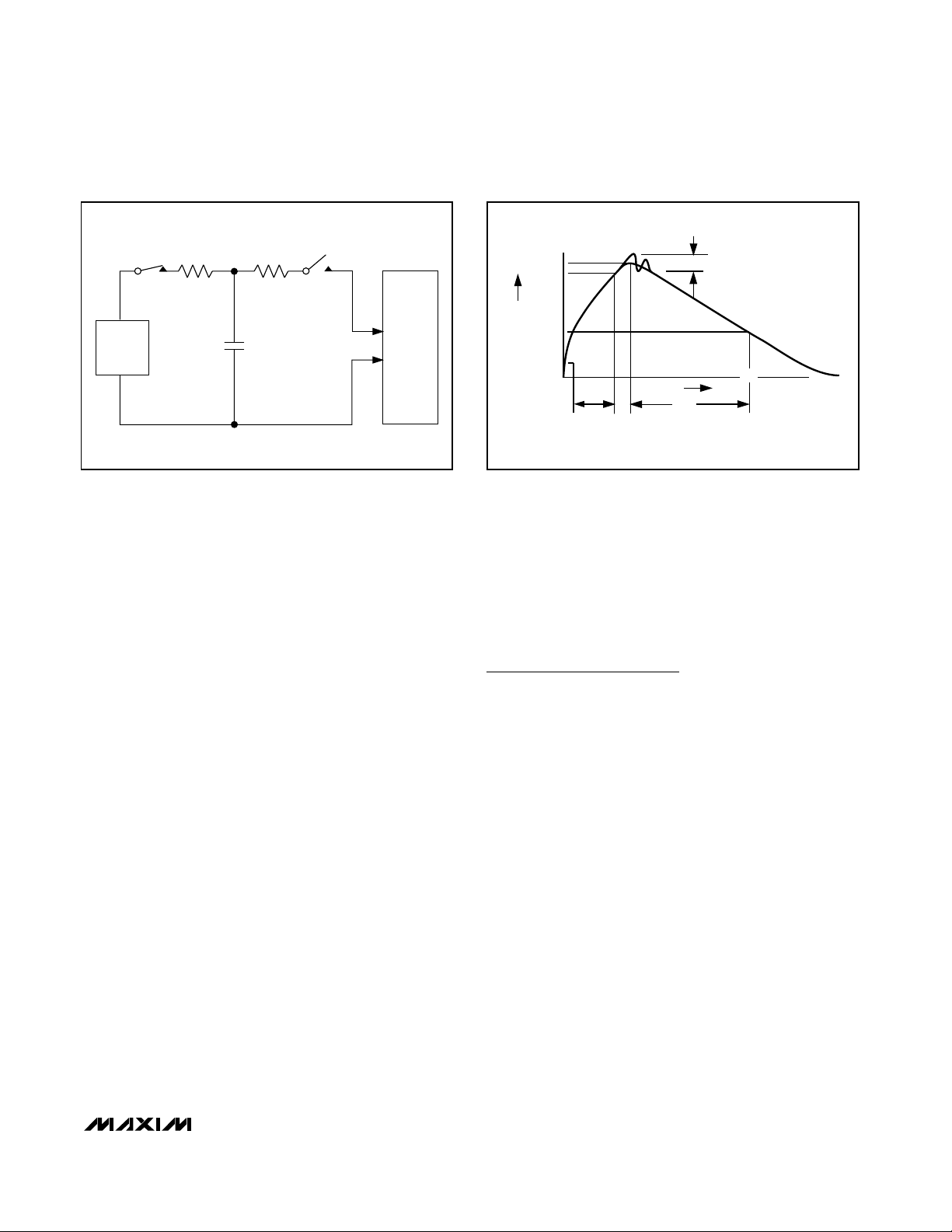
1.5kΩ resistor. Figure 6 shows the current waveform
when the storage capacitor is discharged into a low
impedance.
ESD Test Conditions
ESD performance depends on a variety of conditions.
Please contact Maxim for a reliability report documenting test setup, methodology, and results.
Applications Information
1:2 Multiplexer for Low-Voltage Graphics
Controllers
The MAX4885 provides the level shifting necessary to
drive two standard VGA ports from a graphics controller as low as +2.2V. In 1:2 mode, internal buffers
drive the HSYNC and VSYNC signals to VGA standard
TTL levels. The DDC multiplexer provides level shifting
by clamping signals to a diode drop less than VCL(see
the Typical Operating Circuit). Connect VCLto +3.3V
for normal operation, or to V+ to disable voltage clamping for DDC signals.
EN M SEL FUNCTION
000
1:2 Mode
Buffers Enabled
H0 to H1
V0 to V1
001
1:2 Mode
Buffers Enabled
H0 to H2
V0 to V2
010
2:1 Mode
Buffers Disabled
H0 to H1
V0 to V1
011
2:1 Mode
Buffers Disabled
H0 to H2
V0 to V2
1XX
H_, V_
High Impedance
Table 2. HV Truth Table
X = Don’t Care
EN SEL FUNCTION
00
DDCA0 to DDCA1
DDCB0 to DDCB1
01
DDCA0 to DDCA2
DDCB0 to DDCB2
1X
DDCA_, DDCB_
High Impedance
Table 3. DDC Truth Table
X = Don’t Care
Page 11
MAX4885
Complete VGA 1:2 or 2:1 Multiplexer
______________________________________________________________________________________ 11
2:1 Multiplexer
In 2:1 mode, HSYNC and VSYNC buffers are disabled,
allowing bidirectional signaling. The DDC multiplexer
provides level shifting by clamping signals to a diode
drop less than VCL(see the Typical Operating Circuit).
Connect VCLto V+ to disable voltage clamping for
DDC signals.
Power-Supply Decoupling
Bypass each V+ pin and VCLto ground with a 0.1µF or
larger ceramic capacitor as close to the device as possible.
PC Board Layout
High-speed switches such as the MAX4885 require
proper PC board layout for optimum performance.
Ensure that impedance-controlled PC board traces for
high-speed signals are matched in length and as short
as possible. Connect the exposed pad to a solid
ground plane.
Chip Information
PROCESS: BiCMOS
CONNECT EXPOSED PAD TO GND
CHARGE-CURRENT-
LIMIT RESISTOR
DISCHARGE
RESISTANCE
STORAGE
CAPACITOR
C
s
100pF
R
C
1MΩ
R
D
1500Ω
HIGH-
VOLTAGE
DC
SOURCE
DEVICE
UNDER
TEST
Figure 5. Human Body ESD Test Model
IP 100%
90%
36.8%
t
RL
TIME
t
DL
CURRENT WAVEFORM
PEAK-TO-PEAK RINGING
(NOT DRAWN TO SCALE)
I
r
10%
0
0
AMPERES
Figure 6. HBM Discharge Current Waveform
Page 12

MAX4885
Complete VGA 1:2 or 2:1 Multiplexer
12 ______________________________________________________________________________________
R1
G1
B1
R2
G2
B2
R0
G0
B0
SEL
H0
V0
M
H1
V1
H2
V2
DDCA0
DDCB0
DDCA1
DDCB1
DDCA2
DDCB2
V
CL
QP
VOLTAGE
CLAMP
RGB
CHARGE
PUMP
*
*
MAX4885
EN
Functional Diagram
Page 13

MAX4885
Complete VGA 1:2 or 2:1 Multiplexer
Maxim cannot assume responsibility for use of any circuitry other than circuitry entirely embodied in a Maxim product. No circuit patent licenses are
implied. Maxim reserves the right to change the circuitry and specifications without notice at any time.
Maxim Integrated Products, 120 San Gabriel Drive, Sunnyvale, CA 94086 408-737-7600 ____________________ 13
© 2006 Maxim Integrated Products Printed USA is a registered trademark of Maxim Integrated Products, Inc.
Boblet
Package Information
(The package drawing(s) in this data sheet may not reflect the most current specifications. For the latest package outline information,
go to www.maxim-ic.com/packages
.)
QFN THIN.EPS
D2
(ND-1) X e
e
D
C
PIN # 1
I.D.
(NE-1) X e
E/2
E
0.08 C
0.10 C
A
A1
A3
DETAIL A
E2/2
E2
0.10 M C A B
PIN # 1 I.D.
b
0.35x45°
D/2
D2/2
L
C
L
C
e e
L
CC
L
k
L
L
DETAIL B
L
L1
e
AAAAA
MARKING
I
1
2
21-0140
PACKAGE OUTLINE,
16, 20, 28, 32, 40L THIN QFN, 5x5x0.8mm
-DRAWING NOT TO SCALE-
L
e/2
COMMON DIMENSIONS
MAX.
EXPOSED PAD VARIATIONS
D2
NOM.MIN.
MIN.
E2
NOM. MAX.
NE
ND
PKG.
CODES
1. DIMENSIONING & TOLERANCING CONFORM TO ASME Y14.5M-1994.
2. ALL DIMENSIONS ARE IN MILLIMETERS. ANGLES ARE IN DEGREES.
3. N IS THE TOTAL NUMBER OF TERMINALS.
4. THE TERMINAL #1 IDENTIFIER AND TERMINAL NUMBERING CONVENTION SHALL
CONFORM TO JESD 95-1 SPP-012. DETAILS OF TERMINAL #1 IDENTIFIER ARE
OPTIONAL, BUT MUST BE LOCATED WITHIN THE ZONE INDICATED. THE TERMINAL #1
IDENTIFIER MAY BE EITHER A MOLD OR MARKED FEATURE.
5. DIMENSION b APPLIES TO METALLIZED TERMINAL AND IS MEASURED BETWEEN
0.25 mm AND 0.30 mm FROM TERMINAL TIP.
6. ND AND NE REFER TO THE NUMBER OF TERMINALS ON EACH D AND E SIDE RESPECTIVELY.
7. DEPOPULATION IS POSSIBLE IN A SYMMETRICAL FASHION.
8. COPLANARITY APPLIES TO THE EXPOSED HEAT SINK SLUG AS WELL AS THE TERMINALS.
9. DRAWING CONFORMS TO JEDEC MO220, EXCEPT EXPOSED PAD DIMENSION FOR
T2855-3 AND T2855-6.
NOTES:
SYMBOL
PKG.
N
L1
e
E
D
b
A3
A
A1
k
10. WARPAGE SHALL NOT EXCEED 0.10 mm.
JEDEC
0.70 0.800.75
4.90
4.90
0.25
0.250--
4
WHHB
4
16
0.350.30
5.10
5.105.00
0.80 BSC.
5.00
0.05
0.20 REF.
0.02
MIN. MAX.NOM.
16L 5x5
L
0.30 0.500.40
---
---
WHHC
20
5
5
5.00
5.00
0.30
0.55
0.65 BSC.
0.45
0.25
4.90
4.90
0.25
0.65
--
5.10
5.10
0.35
20L 5x5
0.20 REF.
0.75
0.02
NOM.
0
0.70
MIN.
0.05
0.80
MAX.
---
WHHD-1
28
7
7
5.00
5.00
0.25
0.55
0.50 BSC.
0.45
0.25
4.90
4.90
0.20
0.65
--
5.10
5.10
0.30
28L 5x5
0.20 REF.
0.75
0.02
NOM.
0
0.70
MIN.
0.05
0.80
MAX.
---
WHHD-2
32
8
8
5.00
5.00
0.40
0.50 BSC.
0.30
0.25
4.90
4.90
0.50
--
5.10
5.10
32L 5x5
0.20 REF.
0.75
0.02
NOM.
0
0.70
MIN.
0.05
0.80
MAX.
0.20 0.25 0.30
DOWN
BONDS
ALLOWED
YES3.103.00 3.203.103.00 3.20T2055-3
3.103.00 3.203.103.00 3.20
T2055-4
T2855-3 3.15 3.25 3.35 3.15 3.25 3.35
T2855-6
3.15 3.25 3.35 3.15 3.25 3.35
T2855-4 2.60 2.70 2.80 2.60 2.70 2.80
T2855-5 2.60 2.70 2.80 2.60 2.70 2.80
T2855-7 2.60 2.70
2.80
2.60 2.70 2.80
3.20
3.00 3.10T3255-3 3 3.203.00 3.10
3.203.00 3.10T3255-4 3 3.203.00 3.10
NO
NO
NO
NO
YES
YES
YES
YES
3.203.00T1655-3 3.10 3.00 3.10 3.20 NO
NO3.203.103.003.10T1655N-1 3.00 3.20
3.353.15T2055-5 3.25 3.15 3.25 3.35
YES
3.35
3.15
T2855N-1
3.25 3.15 3.25 3.35
NO
3.353.15T2855-8 3.25 3.15 3.25 3.35
YES
3.203.10T3255N-1 3.00
NO
3.203.103.00
L
0.40
0.40
**
**
**
**
**
**
**
**
**
**
**
**
**
**
SEE COMMON DIMENSIONS TABLE
±0.15
11. MARKING IS FOR PACKAGE ORIENTATION REFERENCE ONLY.
I
2
2
21-0140
PACKAGE OUTLINE,
16, 20, 28, 32, 40L THIN QFN, 5x5x0.8mm
-DRAWING NOT TO SCALE-
12. NUMBER OF LEADS SHOWN ARE FOR REFERENCE ONLY.
3.30T4055-1 3.20 3.40 3.20 3.30 3.40
**
YES
0.050 0.02
0.600.40 0.50
10
-----
0.30
40
10
0.40 0.50
5.10
4.90 5.00
0.25 0.35 0.45
0.40 BSC.
0.15
4.90
0.250.20
5.00 5.10
0.20 REF.
0.70
MIN.
0.75 0.80
NOM.
40L 5x5
MAX.
13. LEAD CENTERLINES TO BE AT TRUE POSITION AS DEFINED BY BASIC DIMENSION "e", ±0.05.
T1655-2
**
YES3.203.103.003.103.00 3.20
T3255-5 YES3.003.103.00
3.20
3.203.10
**
exceptions
 Loading...