

Page 1
General Description
The MAX4881–MAX4884 overvoltage protection (OVP)
controllers with built-in current-limited switch, protect lowvoltage systems against voltages of up to 28V. When the
input voltage exceeds the overvoltage trip level of 5.6V
(MAX4881/MAX4883) or 4.5V (MAX4882/MAX4884), the
external n-channel MOSFET is turned off to prevent damage to the protected components. An undervoltage/overvoltage flag indicator (OV) notifies the processor that an
undervoltage/overvoltage fault condition is present.
The MAX4881/MAX4882 feature an internal 1.1A current-limited switch, while the MAX4883B/MAX4883C/
MAX4884B/MAX4884C include an internal 0.7A currentlimited switch. When the load current is at the current
limit for longer than the blanking time, the switch of the
MAX4881/MAX4882/MAX4883B/MAX4884B latches off
and does not turn back on until EN, CB, or IN is cycled.
A current-limit flag (FLAGI) asserts to indicate a current
fault condition.
The MAX4883C/MAX4884C limit the current to 0.7A
indefinitely until the thermal protection trips. An overcurrent flag output asserts to indicate a current fault condition after the blanking time has elapsed.
The MAX4881–MAX4884 have a control input (CB) that
is used to turn on and off the internal current-limited
switch. Other features include a shutdown function (EN)
to disable the external n-channel MOSFET, and a builtin startup delay to allow the adapter voltage to settle
down before turning on the MOSFET.
The MAX4881–MAX4884 is offered in a space-saving
10-pin TDFN package and is specified for operation
over the extended -40°C to +85°C temperature range.
Applications
Features
♦ Overvoltage Protection Up to 28V
♦ Preset Overvoltage Trip Level
5.6V (MAX4881/MAX4883)
4.5V (MAX4882/MAX4884)
♦ Internal Current-Limited Switch
1.1A (MAX4881/MAX4882)
0.7A (MAX4883/MAX4884)
♦ Drives Low-Cost n-Channel MOSFET
♦ Internal 50ms Startup Delay
♦ Overvoltage Fault OV Indicator
♦ Current-Limit Fault FLAGI Indicator
♦ Undervoltage Lockout
♦ Thermal Shutdown Protection
♦ Tiny 10-Pin TDFN Package
MAX4881–MAX4884
Overvoltage Protection Controllers with
Current Limit in TDFN
________________________________________________________________ Maxim Integrated Products 1
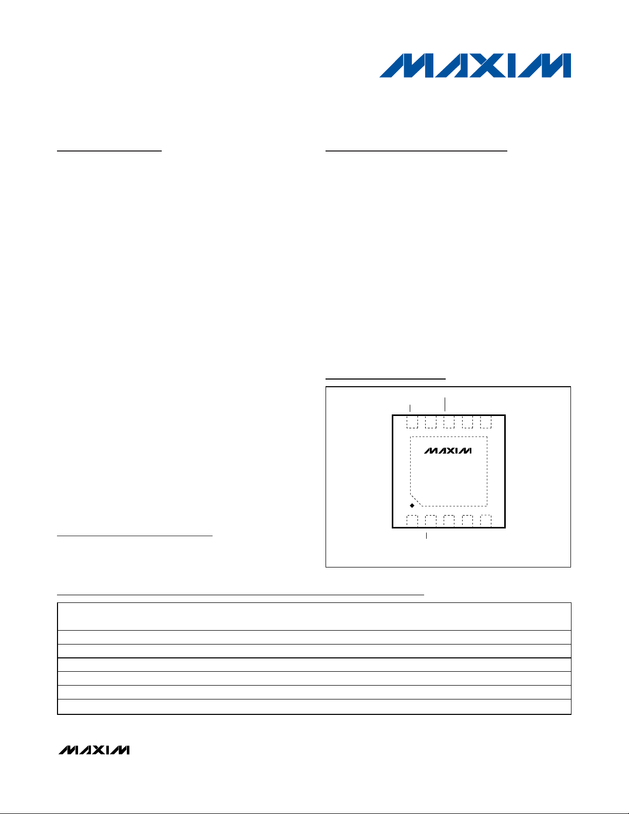
Pin Configuration
Ordering Information
19-3777; Rev 0; 7/05
For pricing, delivery, and ordering information, please contact Maxim/Dallas Direct! at
1-888-629-4642, or visit Maxim’s website at www.maxim-ic.com.
Cell Phones
Digital Still Cameras
PDAs and Palmtop Devices
MP3 Players
* EP = Exposed pad
**Future product—contact factory for availability.
TOP VIEW
OV
10 8 7
134
IN
3mm x 3mm TDFN
N.C.
9
MAX4881
MAX4882
MAX4883
MAX4884
2
EN
FLAGI
GATE
BTB
BTA
GND
6
5
CB
PART TEMP RANGE PIN-PACKAGE
MAX4881ETB -40°C to +85°C 10 TDFN-EP* 5.6 1.1 LATCH-OFF APK
MAX4882ETB -40°C to +85°C 10 TDFN-EP* 4.5 1.1 LATCH-OFF APL
MAX4883BETB -40°C to +85°C 10 TDFN-EP* 5.6 0.7 LATCH-OFF APM
MAX4883CETB** -40°C to +85°C 10 TDFN-EP* 5.6 0.7 CONTINUOUS APN
MAX4884BETB** -40°C to +85°C 10 TDFN-EP* 4.5 0.7 LATCH-OFF APO
MAX4884CETB** -40°C to +85°C 10 TDFN-EP* 4.5 0.7 CONTINUOUS APP
OV TRIP LEVEL
(V)
CURRENT LIMIT
(A)
CURRENT-LIMIT
MODE
TOP
MARK
Page 2
MAX4881–MAX4884
Overvoltage Protection Controllers with
Current Limit in TDFN
2 _______________________________________________________________________________________
ABSOLUTE MAXIMUM RATINGS
ELECTRICAL CHARACTERISTICS
(VIN= +5V (MAX4881/MAX4883), VIN= +4V (MAX4882/MAX4884), TA= -40°C to +85°C, unless otherwise noted. Typical values are
at T
A
= +25°C.) (Note 1)
Stresses beyond those listed under “Absolute Maximum Ratings” may cause permanent damage to the device. These are stress ratings only, and functional
operation of the device at these or any other conditions beyond those indicated in the operational sections of the specifications is not implied. Exposure to
absolute maximum rating conditions for extended periods may affect device reliability.
(All voltages referenced to GND.)
IN ............................................................................-0.3V to +30V
GATE ......................................................................-0.3V to +12V
EN,
CB, OV, FLAGI, BTA, BTB ................................-0.3V to +6V
Continuous Power Dissipation (T
A
= +70°C)
10-Pin TDFN (derate 18.5mW/°C above +70°C) .....1481.5mW
Operating Temperature Range ..........................-40°C to +85°C
Junction Temperature......................................................+150°C
Storage Temperature Range ............................-65°C to +150°C
Lead Temperature (soldering, 10s) ................................+300°C
PARAMETER SYMBOL CONDITIONS MIN TYP MAX UNITS
INPUT VOLTAGE (IN)
Input Voltage Range V
Overvoltage Trip Level OVLO VIN rising
Overvoltage-Trip-Level
Hysteresis
Undervoltage Lockout Threshold UVLO VIN falling
Undervoltage Lockout Hysteresis 50 mV
Supply Current IIN + I
INTERNAL SWITCH
BTA Input Range V
BTA Undervoltage Lockout BTA
BTA-Undervoltage-Lockout
Hysteresis
Switch-Forward Current Limit I
Switch-Reverse Current Limit I
- V
Voltage Drop (V
Blanking Time t
BTB Off Current I
GATE
GATE Voltage V
BTA
)I
BTB
IN
No load, VEN = 0 or 5.5V,
BTA
V
IN
BTA
UVLOVBTA
FWD
REV
BLANK
BTB-OFFVEN
GATE
MAX4881/MAX4882, V
MAX4883/MAX4884, V
MAX4881/MAX4882 1.25
MAX4883/MAX4884 0.775
= 400mA
L
I
GATE
sourcing
1µA
= V
OVLO (MIN)
falling 2.4 2.7 V
= 0, VCB = 0 1 µA
1.2 28 V
MAX4881/MAX4883 5.5 5.6 5.7
MAX4882/MAX4884 4.4 4.5 4.6
50 mV
MAX4881/MAX4883 4.2 4.35 4.5
MAX4882/MAX4884 2.4 2.55 2.7
- 0.1V, VCB = V
BTB
BTB
= 5V
V
BTA
(MAX4881/MAX4883)
V
= 4V
BTA
(MAX4882/MAX4884)
VIN = 5V (MAX4881/MAX4883) 9 10
V
= 4.3V
IN
(MAX4882/MAX4884)
IN
2.8 5.7 V
= GND 1 1.1 1.25
= GND 0.6 0.7 0.775
20 50 80 ms
7.6 8.6
240 380 µA
50 mV
110
110
V
V
A
A
mV
V
Page 3
MAX4881–MAX4884
Overvoltage Protection Controllers with
Current Limit in TDFN
_______________________________________________________________________________________ 3
ELECTRICAL CHARACTERISTICS (continued)
(VIN= +5V (MAX4881/MAX4883), VIN= +4V (MAX4882/MAX4884), TA= -40°C to +85°C, unless otherwise noted. Typical values are
at T
A
= +25°C.) (Note 1)
Note 1: All devices are 100% tested at T
A
= +25°C. Electrical limits over the full temperature range are guaranteed by design.
PARAMETER SYMBOL CONDITIONS MIN TYP MAX UNITS
INPUT VOLTAGE (IN)
Input Voltage Range V
Overvoltage Trip Level OVLO VIN rising
Overvoltage-Trip-Level
Hysteresis
Undervoltage Lockout Threshold UVLO VIN falling
Undervoltage Lockout Hysteresis 50 mV
Supply Current IIN + I
INTERNAL SWITCH
BTA Input Range V
BTA Undervoltage Lockout BTA
BTA-Undervoltage-Lockout
Hysteresis
Switch-Forward Current Limit I
Switch-Reverse Current Limit I
Voltage Drop (V
Blanking Time t
BTB Off Current I
GATE
GATE Voltage V
BTA
- V
)I
BTB
IN
No load, VEN = 0 or 5.5V,
BTA
V
IN
BTA
UVLOVBTA
FWD
REV
BLANK
BTB-OFFVEN
GATE
MAX4881/MAX4882, V
MAX4883/MAX4884, V
MAX4881/MAX4882 1.25
MAX4883/MAX4884 0.775
= 400mA
L
I
GATE
sourcing
1µA
MAX4881/MAX4883 5.5 5.6 5.7
MAX4882/MAX4884 4.4 4.5 4.6
MAX4881/MAX4883 4.2 4.35 4.5
MAX4882/MAX4884 2.4 2.55 2.7
= V
OVLO (MIN)
falling 2.4 2.7 V
= 0, VCB = 0 1 µA
- 0.1V, VCB = V
BTB
BTB
V
= 5V
BTA
(MAX4881/MAX4883)
V
= 4V
BTA
(MAX4882/MAX4884)
VIN = 5V (MAX4881/MAX4883) 9 10
V
= 4.3V
IN
(MAX4882/MAX4884)
IN
= GND 1 1.1 1.25
= GND 0.6 0.7 0.775
1.2 28 V
50 mV
240 380 µA
2.8 5.7 V
50 mV
110
mV
110
20 50 80 ms
7.6 8.6
V
V
A
A
V
Page 4
MAX4881–MAX4884
Overvoltage Protection Controllers with
Current Limit in TDFN
4 _______________________________________________________________________________________
Typical Operating Characteristics
(VIN= 5V, TA= +25°C, unless otherwise noted.)
GATE VOLTAGE vs. INPUT VOLTAGE
(MAX4881)
INPUT VOLTAGE (V)
GATE VOLTAGE (V)
MAX4881 toc04
012345678
0
3
6
9
12
OVLO TRIP POINT
UVLO TRIP POINT
BTB OFF CURRENT vs. TEMPERATURE
TEMPERATURE (°C)
BTB OFF CURRENT (nA)
MAX4881 toc05
-40 -15 10 35 60 85
0.01
0.1
1
10
100
1000
VEN = 0
V
CB
= 0
V
BTB
= 5.5V
POWER-UP RESPONSE (MAX4884)
MAX4881 toc06
20ms/div
5V
10V
5V
0
0
5V
0
IN
GATE
BTA
OV
POWER-DOWN RESPONSE (MAX4884)
MAX4881 toc07
20ms/div
5V
0
5V
0
5V
0
IN
10V
GATE
0
BTA
OV
OVERVOLTAGE RESPONSE (MAX4884)
MAX4881 toc09
400ns/div
6V
3V
0
5V
0
IN
GATE
OV
20mA
I
GATE
EN vs. GATE (MAX4884)
MAX4881 toc08
100µs/div
5V
0
10V
0
EN
GATE
IIN + I
BTA
CURRENT vs. INPUT VOLTAGE
INPUT VOLTAGE (V)
I
IN
+ I
BTA
CURRENT (µA)
MAX4881 toc01
0 5 10 15 20 25 30
0
50
100
150
200
250
300
350
400
VEN = 0
V
CB
= 5V
OVLO TRIP POINT
UVLO TRIP POINT
IIN + I
BTA
CURRENT vs. TEMPERATURE
TEMPERATURE (°C)
I
IN
+ I
BTA
CURRENT (µA)
MAX4881 toc02
-40 -15 10 35 60 85
0
50
100
150
200
250
300
350
400
GATE VOLTAGE vs. INPUT VOLTAGE
(MAX4884)
INPUT VOLTAGE (V)
GATE VOLTAGE (V)
MAX4881 toc03
012345678
0
3
6
9
12
UVLO TRIP POINT
OVLO TRIP POINT
Page 5

MAX4881–MAX4884
Overvoltage Protection Controllers with
Current Limit in TDFN
_______________________________________________________________________________________ 5
Typical Operating Characteristics (continued)
(VIN= 5V, TA= +25°C, unless otherwise noted.)
CURRENT LIMIT vs. TEMPERATURE
(MAX4884)
800
700
600
500
400
300
CURRENT LIMIT (mA)
200
VIN = 4.4V
= 2.7V
V
BTB
100
= 5V
V
CB
0
-40 -15 10 35 60 85
TEMPERATURE (°C)
CURRENT LIMIT vs. V
BTB
(MAX4884)
800
700
600
500
400
300
CURRENT LIMIT (mA)
200
VIN = 4.4V
100
= 5V
V
CB
0
012345
V
(V)
BTB
CURRENT LIMIT vs. TEMPERATURE
1.25
MAX4881 toc10
1.00
0.75
0.50
CURRENT LIMIT (A)
VIN = 5V
0.25
V
BTB
V
CB
0
-40 -15 10 35 60 85
1.25
MAX4881 toc12
1.00
0.75
0.50
CURRENT LIMIT (A)
0.25
VIN = 5V
= 5V
V
CB
0
012345
(MAX4881)
= 2.7V
= 5V
TEMPERATURE (°C)
CURRENT LIMIT vs. V
(MAX4881)
V
(V)
BTB
BTB
MAX4881 toc11
MAX4881 toc13
Page 6

MAX4881–MAX4884
Overvoltage Protection Controllers with
Current Limit in TDFN
6 _______________________________________________________________________________________
Pin Description
PIN NAME FUNCTION
1IN
2 EN
3 GATE
4 BTA
Input. IN is the power input for the OVP charge pump. Bypass IN to GND with a 1µF capacitor or
larger.
Active-Low Enable Input. Drive EN high to turn off the external MOSFET. Driving EN low activates
the OVP circuitry and turns on the external MOSFET.
Gate Drive Output. GATE is the output of an on-chip OVP charge pump. When V
, GATE is driven high to turn on the external n-channel MOSFET.
V
OVLO
Internal Current-Limited Switch Terminal. Connect BTA to the source of the external n-channel
MOSFET. BTA is the power input for the entire device (except the OVP charge pump). Bypass BTA
to GND with a 0.1µF capacitor as close to the device as possible for proper operation.
UVLO
< VIN <
5CB
6 GND Ground
7 BTB
8 FLAGI
9 N.C. No Connection. Not internally connected.
10 OV
—EP
Active-Low Internal Current-Limited-Switch Control Input. Drive CB high to turn on the internal
switch, pull CB low to turn off the internal switch.
Internal Current-Limited-Switch Output. Bypass BTB to GND with 0.1µF capacitor as close to the
device as possible.
Active-Low Open-Drain Internal Current-Limited Flag Output. FLAGI asserts low when the current
is at the limit for longer than the blanking time. FLAGI is disabled when EN goes high.
Active-Low Open-Drain IN-Overvoltage Flag Output. OV goes low when an
undervoltage/overvoltage fault occurs at IN. OV is disabled when EN goes high.
Exposed Pad. EP is internally connected to GND. Do not use EP as the only electrical ground
connection.
Page 7

Detailed Description
The MAX4881–MAX4884 provide up to +28V overvoltage protection for low-voltage systems. When the input
voltage at IN exceeds the overvoltage trip level (OVLO),
the MAX4881–MAX4884 turn off the low-cost external nchannel FET to prevent damage to the protected components and issue an overvoltage fault flag.
The MAX4881–MAX4884 feature a built-in current-limited
switch that limits the load current to 1.1A (MAX4881/
MAX4882) and 0.7A (MAX4883B/MAX4883C/MAX4884B/
MAX4884C). When the load current is at the current limit
for longer than the blanking time, the switch of the
MAX4881/MAX4882/MAX4883B/MAX4884B latches off
and does not turn back on until EN or CB or IN is cycled.
A current-limit flag (FLAGI) asserts to indicate a current
fault condition. The MAX4883C/MAX4884C limit the current to 0.7A indefinitely until the thermal protection trips.
An overcurrent flag output asserts to indicate a current
fault condition after the blanking time has elapsed.
IN-Undervoltage Lockout (UVLO)
The MAX4881/MAX4883 have a fixed 4.35V undervoltage lockout level (UVLO) while the MAX4882/MAX4884
have a fixed UVLO of 2.55V. GATE goes low when V
IN
is below V
UVLO
, turning off the external n-channel FET.
IN-Overvoltage Lockout (OVLO)
The MAX4881/MAX4883 have a fixed 5.6V overvoltage
threshold (OVLO), while the MAX4882/MAX4884 have a
fixed OVLO of 4.5V. GATE goes low when VINis higher
than V
OVLO
, turning off the external n-channel FET.
Fault Flag Output (OV)
The OV output signals the host system that there is a fault
with the input voltage. OV asserts low in response to
either an overvoltage or undervoltage fault. OV stays low
for 50ms after GATE turns on, before deasserting high.
OV is an open-drain active-low output. Connect a
pullup resistor from OV to the logic I/O voltage of the
host system, or to any voltage source up to 6V. Driving
EN high disables OV.
MAX4881–MAX4884
Overvoltage Protection Controllers with
Current Limit in TDFN
_______________________________________________________________________________________ 7
V
Figure 1. Startup Timing Diagram
Figure 2. Shutdown Timing Diagram
Figure 3. Power-Up Overvoltage Timing Diagram
Figure 4. Disable Timing Diagram
V
1.2V
GATE
V
t
0.3V
GON
5V
8V
t
0V-BLANK
2.4V
I
GATE
V
IN
0V
V
OVLO
t
OVP
80%
V
IN
OV
UVLO
t
START
7V/8V
V
IN
4V/5V
V
GATE
V
OV
V
OVLO
t
GOFF
0.3V
t
OV
0.4V
V
EN
V
GATE
2.4V
t
DIS
0.3V
Page 8

MAX4881–MAX4884
Overcurrent Flag Output (
FLAGI
)
The MAX4881–MAX4884 have an overcurrent-fault flag
output (FLAGI) to indicate a current fault condition.
FLAGI asserts low to indicate a fault when the current
reaches the current limit for longer than the 50ms blanking time. Toggle IN or CB or EN to release FLAGI latched
condition. FLAGI does not assert if the current-limit fault
occurs for less than the blanking time (Figure 5).
FLAGI is disabled when EN goes high. When CB is low,
the switch opens, but FLAGI is not active.
FLAGI is an open-drain active-low output. Connect a
pullup resistor from FLAGI to the logic I/O voltage of the
host system, or to any voltage source up to 6V.
Overvoltage Protection Controllers with
Current Limit in TDFN
8 _______________________________________________________________________________________
Figure 5. Current-Limit Fault Timing
Figure 6. Latch-Off Fault Blanking (MAX4881/MAX4882/
MAX4883B/MAX4884B
t
BLANK
LOAD
CURRENT
ON
SWITCH
STATUS
FLAGI
(a) MAX4881/MAX4882/MAX4883B/MAX4884B
t
BLANK
LOAD
CURRENT
SWITCH
STATUS
FLAGI
ON
t
BLANK
t
BLANK
OFF
CURRENT
LIMIT
CURRENT
LIMIT
LOAD
CURRENT
SWITCH
STATUS
EN
STATUS
FLAGI
PIN STATUS
LOAD
CURRENT
SWITCH
STATUS
STATUS
t
BLANK
ON
OFF
t
BLANK
ON
OFF
CB
(a)
t
BLANK
t
BLANK
FLAGI
(b) MAX4883C/MAX4884C
STATUS
LOAD
CURRENT
SWITCH
STATUS
OFF
(b)
t
BLANK
ON
t
BLANK
STATUS
FLAGI
STATUS
IN
UVLO
(c)
Page 9

Current-Limit Switch
When the forward- or reverse-current-limit threshold is
exceeded, t
BLANK
timer begins counting. The timer
resets if the overcurrent condition disappears before
t
BLANK
has elapsed. The internal switch is latched off if
the overcurrent condition continues up to the end of the
blanking time (MAX4881/MAX4882/MAX4883B/
MAX4884B). The MAX4883C/MAX4884C limit the current infinitely until the thermal trip point occurs. Reset
the switch by toggling EN or CB or IN (Figure 6).
EN
Input
The MAX4881–MAX4884 feature an active-low enable
input (EN). Drive EN low or connect to ground for normal operation. Drive EN high to force the external nchannel MOSFET off, and to disable OV and FLAGI.
GATE Driver
An on-chip charge pump drives the GATE voltage to
about twice above VIN, allowing the use of a low-cost nchannel MOSFET (Figure 7). The actual GATE output
voltage tracks approximately 2 x VINuntil VINexceeds
the OVLO trip level, 5.6V (MAX4881/MAX4883) and
4.5V (MAX4882/MAX4884) typically. The GATE output
voltage, as a function of input voltage, is shown in the
Typical Operating Characteristics.
Applications Information
MOSFET Selection
The MAX4881–MAX4884 are designed for use with
an n-channel MOSFET. MOSFETs with R
DS(ON)
, specified for a VGSof 4.5V or less, work well. If the input supply is near the UVLO minimum of 4.2V (MAX4881/
MAX4883), or of 2.4V (MAX4882/MAX4884), consider
using a MOSFET specified for a lower VGSvoltage. Also,
the VDSshould be 30V for the MOSFET to withstand the
full 28V IN range of the MAX4881–MAX4884. Table 1
shows a selection of MOSFETs appropriate for use with
the MAX4881–MAX4884.
IN Bypass Considerations
Bypass IN to GND with a 1µF ceramic capacitor to
achieve 15kV ESD-protected input. When the power
MAX4881–MAX4884
Overvoltage Protection Controllers with
Current Limit in TDFN
_______________________________________________________________________________________ 9
Figure 7a. MAX4881/MAX4882/MAX4883B/MAX4884B
Functional Diagram
Figure 7b. MAX4883C/MAX4884C Functional Diagram
OV
FLAGI
EN
IN
IN
OVLO
UVLO
I
REF
AND LATCH-OFF LOGIC
1.1A/0.7A
LIMIT
CHARGE
PUMP
BLANKING TIME
GATE
CHARGE PUMP
MAX4881/MAX4882
MAX4883B/MAX4884B
GND
BTA
UVLO
IN
BTA
OV
FLAGI
BTB
CB
EN
IN
OVLO
UVLO
1.1A/0.7A
LIMIT
I
REF
CHARGE
PUMP
BLANKING TIME
LOGIC
GATE
CHARGE PUMP
BTA
UVLO
MAX4883C/MAX4884C
GND
BTA
BTB
CB
Page 10
source has significant inductance due to long lead
length, take care to prevent overshoots due to the LC
tank circuit, and provide protection if necessary to prevent exceeding the 30V absolute maximum rating on IN.
The MAX4881–MAX4884 provide protection against
voltage faults up to 28V, but this does not include negative voltages. If negative voltages are a concern, connect a Schottky diode from IN to GND to clamp
negative input voltages.
Exposed Pad
The MAX4881–MAX4884 provide an exposed pad on the
bottom of the package. This pad is internally connected
to GND. For the best thermal conductivity and higher
power dissipation, solder the exposed pad to the ground
plane. Do not use the ground-connected pad as the only
MAX4881–MAX4884
Overvoltage Protection Controllers with
Current Limit in TDFN
10 ______________________________________________________________________________________
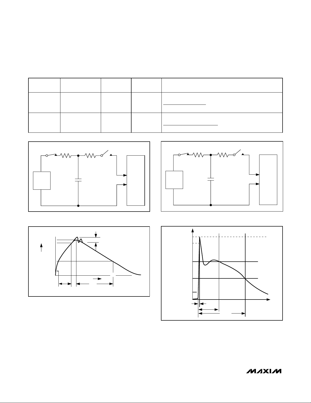
Figure 10. IEC 61000-4-2 ESD Test Model
Figure 8. Human Body ESD Test Model
Figure 9. Human Body Model Current Waveform
Figure 11. IEC 61000-4-2 ESD Generator Current
Table 1. MOSFET Suggestions
PART
CONFIGURATION/
PACKAGE
V
DS
MAX (V)
Si1426DH Single/SC70-6 30 115
FDG315N Single/SC70-6 30 160
R
ON
AT 4.5V (mΩ)
MANUFACTURER
Vishay Siliconix
http://www.vishay.com
(402) 563-6866
Fairchild Semiconductor
http://www.fairchildsemi.com
(207) 775-8100
R
C
1MΩ
CHARGE-CURRENT-
LIMIT RESISTOR
HIGH-
VOLTAGE
DC
SOURCE
100pF
C
s
R
D
1.5kΩ
DISCHARGE
RESISTANCE
STORAGE
CAPACITOR
PEAK-TO-PEAK RINGING
I
r
(NOT DRAWN TO SCALE)
AMPERES
IP 100%
90%
36.8%
10%
0
0
t
RL
TIME
t
DL
CURRENT WAVEFORM
DEVICE
UNDER
TEST
HIGH-
VOLTAGE
DC
SOURCE
R
C
50Ω to 100Ω
CHARGE-CURRENT-
LIMIT RESISTOR
C
150pF
s
RD
330Ω
DISCHARGE
RESISTANCE
STORAGE
CAPACITOR
I
100%
90%
PEAK
I
10%
DEVICE
UNDER
TEST
tr = 0.7ns to 1ns
30ns
60ns
t
Page 11

electrical ground connection or ground return. Use GND
(pin 6) as the only electrical ground connection.
ESD Test Conditions
ESD performance depends on a number of conditions.
The MAX4881–MAX4884 is specified for 15kV typical
ESD resistance on IN when IN is bypassed to ground
with a 1µF low-ESR ceramic capacitor. Contact Maxim
for a reliability report that documents test setup,
methodology, and results.
Human Body Model
Figure 8 shows the Human Body Model and Figure 9
shows the current waveform it generates when discharged into a low impedance. This model consists of
a 100pF capacitor charged to the ESD voltage of interest, which is then discharged into the device through a
1.5kΩ resistor.
IEC 61000-4-2
Since January 1996, all equipment manufactured
and/or sold in the European community has been
required to meet the stringent IEC 61000-4-2 specification. The IEC 61000-4-2 standard covers ESD testing
and performance of finished equipment; it does not
specifically refer to integrated circuits. The
MAX4881–MAX4884 help users design equipment that
meets Level 3 of IEC 61000-4-2, without additional
ESD-protection components.
The main difference between tests done using the
Human Body Model and IEC 61000-4-2 is higher peak
current in IEC 61000-4-2. Because series resistance is
lower in the IEC 61000-4-2 ESD test model (Figure 10),
the ESD-withstand voltage measured to this standard is
generally lower than that measured using the Human
Body Model. Figure 11 shows the current waveform for
the ±8kV, IEC 61000-4-2, Level 4, ESD Contact
Discharge test. The Air-Gap test involves approaching
the device with a charger probe. The Contact
Discharge method connects the probe to the device
before the probe is energized.
Typical Operating Circuits
Figures 12 and 13 depict some typical connections to
the MAX4881–MAX4884. Figure 12 shows a battery
charger application where the source power is an 4.4V
adapter with a built-in charger, while Figure 13 shows
an application where the battery charger is external.
Chip Information
TRANSISTOR COUNT: 2391
PROCESS: BiCMOS
MAX4881–MAX4884
Overvoltage Protection Controllers with
Current Limit in TDFN
______________________________________________________________________________________ 11
Figure 13. Connection to an AC-DC Adapter with a Built-In
Battery Charger
4.4V ADAPTER
Figure 12. Connection to an AC-DC Adapter without a Built-In
Battery Charger
WITH BUILT-IN
CHARGER
AC-DC
ADAPTER
5.25V
GATEIN
BTA
V
IO
FLAGI
OV
CB
EN
MAX4882/
MAX4884
1.1A/0.7A
GND
BTB
LOAD
Li+
GATEIN
BTA
V
IO
FLAGI
OV
CB
EN
MAX4881/
MAX4883
1.1A/0.7A
GND
BTB
BATTERY
CHARGER
LOAD
Li+
Page 12
MAX4881–MAX4884
Overvoltage Protection Controllers with
Current Limit in TDFN
Maxim cannot assume responsibility for use of any circuitry other than circuitry entirely embodied in a Maxim product. No circuit patent licenses are
implied. Maxim reserves the right to change the circuitry and specifications without notice at any time.
12 ____________________Maxim Integrated Products, 120 San Gabriel Drive, Sunnyvale, CA 94086 408-737-7600
© 2005 Maxim Integrated Products Printed USA is a registered trademark of Maxim Integrated Products. Inc.
Jackson
Maxim cannot assume responsibility for use of any circuitry other than circuitry entirely embodied in a Maxim product. No circuit patent licenses are
implied. Maxim reserves the right to change the circuitry and specifications without notice at any time.
12 ____________________Maxim Integrated Products, 120 San Gabriel Drive, Sunnyvale, CA 94086 408-737-7600
© 2005 Maxim Integrated Products Printed USA is a registered trademark of Maxim Integrated Products. Inc.
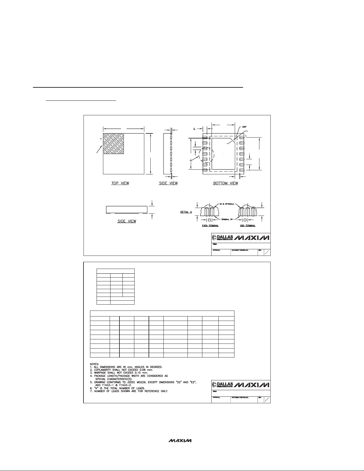
Package Information
(The package drawing(s) in this data sheet may not reflect the most current specifications. For the latest package outline information
go to www.maxim-ic.com/packages
.)
Maxim cannot assume responsibility for use of any circuitry other than circuitry entirely embodied in a Maxim product. No circuit patent licenses are
implied. Maxim reserves the right to change the circuitry and specifications without notice at any time.
12 ____________________Maxim Integrated Products, 120 San Gabriel Drive, Sunnyvale, CA 94086 408-737-7600
© 2005 Maxim Integrated Products Printed USA is a registered trademark of Maxim Integrated Products. Inc.
D
PIN 1
INDEX
AREA
-DRAWING NOT TO SCALE-
COMMON DIMENSIONS
MIN. MAX.
SYMBOL
A
0.70 0.80
D
2.90 3.10
E 2.90 3.10
A1
0.00 0.05
L
0.20 0.40
0.25 MIN.k
A2 0.20 REF.
A2
N
b
E
A1
A
DETAIL A
E2
L
D2
0.35x0.35
k
C
L
e
PACKAGE OUTLINE, 6,8,10 & 14L,
TDFN, EXPOSED PAD, 3x3x0.80 mm
21-0137
PIN 1 ID
[(N/2)-1] x e
e
C
L
e
REF.
L
1
G
2
6, 8, &10L, DFN THIN.EPS
PACKAGE VARIATIONS
PKG. CODE
T633-2 6 1.50±0.10 2.30±0.10 0.95 BSC
T833-2 8 1.50±0.10 2.30±0.10
T833-3 8 1.50±0.10 2.30±0.10
-DRAWING NOT TO SCALE-
N
D2 E2 e
1.50±0.10
1.50±0.10
1.70±0.10 2.30±0.1014T1433-1
2.30±0.101.50±0.106T633-1 0.95 BSC MO229 / WEEA 1.90 REF0.40±0.05
2.30±0.108T833-1
2.30±0.1010T1033-1
JEDEC SPEC
MO229 / WEEA
0.65 BSC
MO229 / WEEC
0.65 BSC MO229 / WEEC
0.65 BSC MO229 / WEEC
0.50 BSC
MO229 / WEED-3
0.40 BSC
0.40 BSC
- - - - 0.20±0.05 2.40 REFT1433-2 14 2.30±0.101.70±0.10
b
0.40±0.05 1.90 REF
0.30±0.05 1.95 REF
0.30±0.05 1.95 REF
DOWNBONDS
[(N/2)-1] x e
ALLOWED
1.95 REF0.30±0.05
2.00 REF0.25±0.05
2.40 REF0.20±0.05- - - -
PACKAGE OUTLINE, 6,8,10 & 14L,
TDFN, EXPOSED PAD, 3x3x0.80 mm
YES
YES
NO
NO
NO
NO
NO
NO
2
21-0137
G
2
 Loading...