

Page 1
General Description
The MAX4880 is an overvoltage-protection controller
with an internal current-limited switch that can be configured as a low-cost battery charger. When the input
voltage exceeds the overvoltage trip level (5.7V), or
drops below the undervoltage-lockout level (4.2V), the
MAX4880 turns off the external n-channel MOSFET and
asserts an undervoltage/overvoltage flag indicator
(FLAGV) low to notify the processor.
The MAX4880 internal current-limited switch limits the
charge current flowing to the battery to 525mA. The
switch opens when the battery voltage reaches its fullcharged state (4.2V), and a flag (BAT_OK) asserts to
notify the processor. The MAX4880 includes a switchcontrol input (CB) to turn off the internal current-limited
switch, regardless of the battery voltage.
The MAX4880 also features a built-in startup delay that
allows the adapter voltage to settle down before turning
on the MOSFET. Other features include 15kV ESD protection for the input and a shutdown function (EN) to
turn off the external n-channel MOSFET.
The MAX4880 is available in a space-saving 10-pin
TDFN package and is specified for operation over the
extended -40°C to +85°C temperature range.
Applications
Cell Phones
Digital Still Cameras
PDAs and Palmtop Devices
MP3 Players
Features
♦ Overvoltage Protection Up to 28V
♦ Preset 5.6V Overvoltage Trip Level
♦ Internal 525mA Current-Limited Switch
♦ ±1.2% Accurate Battery Disconnect (4.2V)
♦ Drives Low-Cost n-Channel MOSFET
♦ Internal 50ms Startup Delay
♦ Overvoltage/Undervoltage-Fault FLAGV Indicator
♦ Battery-Voltage-Trip BAT_OK Indicator
♦ Undervoltage Lockout
♦ Thermal Shutdown Protection
♦ Tiny 10-Pin TDFN Package
MAX4880
Overvoltage-Protection Controller with
Internal Disconnect Switch
________________________________________________________________ Maxim Integrated Products 1
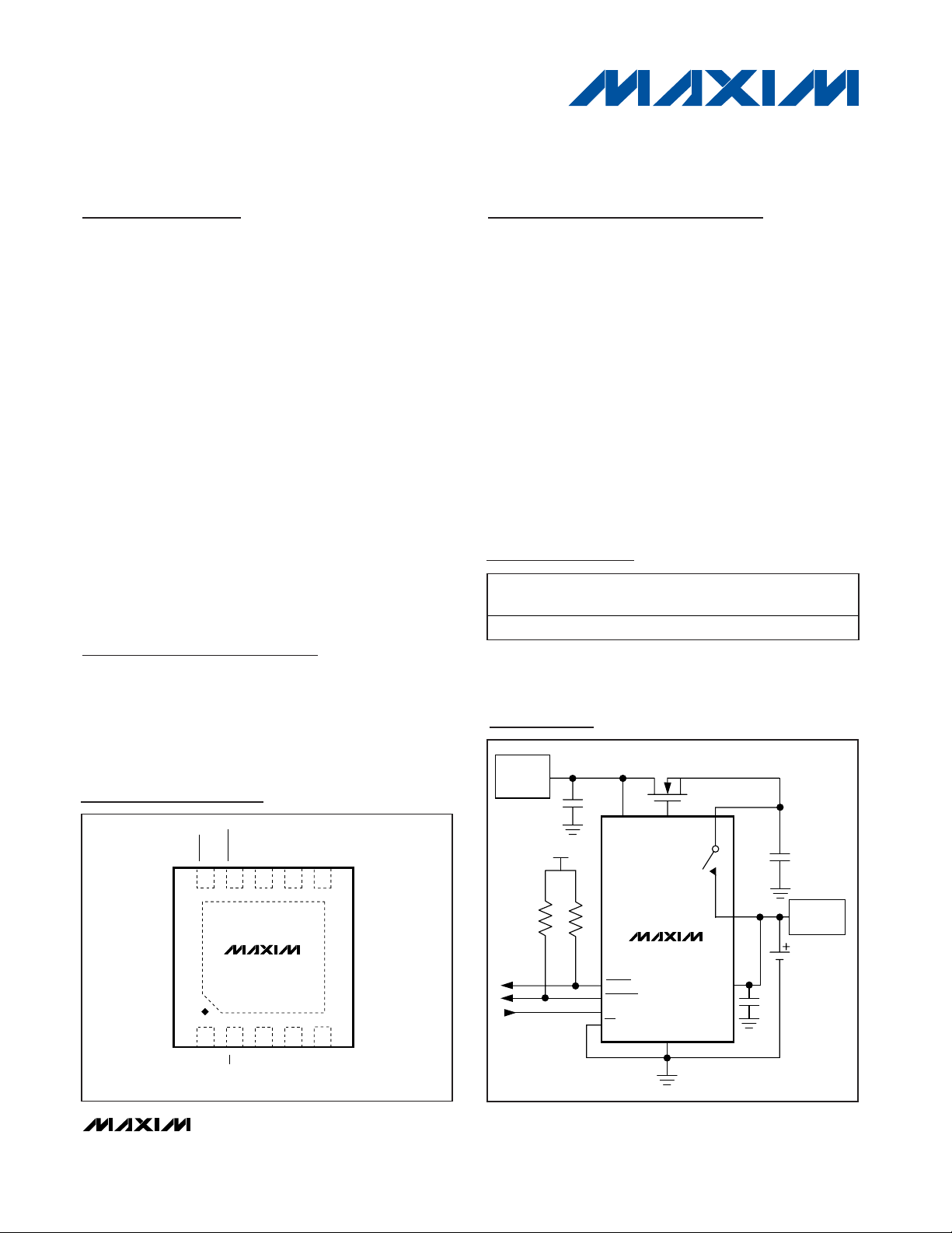
FLAGV
GND
BTB
BTB_SNS
MAX4880
BAT_OK
IN
GATE
BTA
EN
3mm x 3mm TDFN
TOP VIEW
CB
134
10 8 7
2
9
5
6
Pin Configuration
Ordering Information
AC-DC
ADAPTER
5.25V
GATEIN
FLAGV
BAT_OK
BTB_SNS
Li+
BTB
BTA
CB
EN
GND
DC-DC
CONVERTER
V
IO
MAX4880
Typical Operating Circuit
19-3776; Rev 0; 7/05
For pricing, delivery, and ordering information, please contact Maxim/Dallas Direct! at
1-888-629-4642, or visit Maxim’s website at www.maxim-ic.com.
PART
TEMP RANGE
PINPACKAGE
TOP
MARK
MAX4880ETB
APJ
* EP = Exposed Pad
-40°C to +85°C 10 TDFN-EP*
Page 2

MAX4880
Overvoltage-Protection Controller with
Internal Disconnect Switch
2 _______________________________________________________________________________________
ABSOLUTE MAXIMUM RATINGS
ELECTRICAL CHARACTERISTICS
(VIN= 5V, TA= -40°C to +85°C, unless otherwise noted. Typical values are at TA= +25°C.) (Note 1)
Stresses beyond those listed under “Absolute Maximum Ratings” may cause permanent damage to the device. These are stress ratings only, and functional
operation of the device at these or any other conditions beyond those indicated in the operational sections of the specifications is not implied. Exposure to
absolute maximum rating conditions for extended periods may affect device reliability.
(All voltages referenced to GND.)
IN ............................................................................-0.3V to +30V
GATE ......................................................................-0.3V to +12V
EN, CB, FLAGV, BAT_OK, BTA, BTB, BTB_SNS .....-0.3V to +6V
Continuous Power Dissipation (T
A
= +70°C)
10-Pin TDFN (derate 18.5mW/°C above +70°C) ...1481.5mW
Operating Temperature Range ...........................-40°C to +85°C
Junction Temperature .................................................... +150°C
Storage Temperature Range ............................-65°C to +150°C
Lead Temperature (soldering, 10s) ................................+300°C
PARAMETER
SYMBOL
CONDITIONS
MIN
TYP
MAX
UNITS
INPUT VOLTAGE (IN)
Input Voltage Range V
IN
1.2
V
Overvoltage Trip Level OVLO VIN rising 5.5 5.6 5.7 V
O ver vol tag e- Tr i p - Level H yster esi s
50 mV
Undervoltage-Lockout Threshold
UVLO VIN falling 4.2
4.5 V
Undervoltage-Lockout Hysteresis
50 mV
Supply Current
No load, VIN = 5.4V, VEN = 0 or 5.5V,
V
CB
= 0 or V
IN
380 µA
INTERNAL SWITCH
BTA Input Range V
BTA
2.8 5.7 V
BTA Undervoltage Lockout
Falling edge 2.4 2.7 V
BTA-Undervoltage-Lockout
Hysteresis
50 mV
BTB-Switch-Disconnect Trip
Level
V
BTB-Switch-Disconnect
Hysteresis
mV
Switch-Forward Current Limit I
FWD
600 mA
TA = +25°C 600
Switch-Reverse Current Limit I
REV
650
mA
Voltage Drop (V
BTA
– V
BTB
)I
L
= 400mA 110 mV
BTB Off Current
V EN = 0 ( V
C B
= 0, or V
IN
< V
U V L O
and V
BTA
= 0)
1µA
GATE
GATE Voltage V
GATEIGATE
sourcing 1µA , VIN = 5V 9 10 V
GATE Pulldown Current I
PD
VIN > V
OVLO
, V
GATE
= 5V 60 mA
TIMING
GATE Startup Delay t
START
VIN > V
UVLO
, V
GATE
> 0.3V (Figure 1) 20 50 80 ms
FLAGV Delay Time t
DELAYVGATE
= 0.3V,V
FLAGV
= 2.4V (Figure 1) 20 50 80 ms
GATE Turn-On Time t
GON
7ms
GATE Turn-Off Time t
GOFF
VIN increasing from 5V to 8V at 3V/µs,
V
GATE
= 0.3V, C
GATE
= 1500pF (Figure 2)
620µs
I
+ I
IN
BTA
UVLO
BTB
TRIP
I
BTB-OFF
BTA
V
= 0.3V to 8V , C
GAT E
4.35
240
4.10 4.20
200
450 525
= 1500p F ( Fi g ur e 1)
GAT E
28.0
Page 3
MAX4880
Overvoltage-Protection Controller with
Internal Disconnect Switch
_______________________________________________________________________________________ 3
Note 1: All devices are 100% tested at TA= +25°C. Electrical limits over the full temperature range are guaranteed by design.
ELECTRICAL CHARACTERISTICS (continued)
(VIN= 5V, TA= -40°C to +85°C, unless otherwise noted. Typical values are at TA= +25°C.) (Note 1)
PARAMETER
SYMBOL
CONDITIONS
MIN
TYP
MAX
UNITS
FLAGV Assertion Delay t
FLAGV
VIN increasing from 5V to 8V at 3V/µs,
V
FLAGV
= 0.4V (Figure 2)
5.8 µs
Initial Overvoltage Fault Delay t
OVP
VIN increasing from 0 to 8V,
I
GATE
= 80% of IPD (Figure 3)
ns
Disable Time t
DIS
VEN = 2.4V, V
GATE
= 0.3V (Figure 4)
ns
EN, CB INPUTS
Input-High Voltage V
IH
1.4 V
Input-Low Voltage V
IL
0.5 V
Input Leakage 1µA
FLAGV, BAT_OK OUTPUTS
Output Voltage Low V
OL
I
SINK
= 1mA, FLAGV, BAT_OK assert 0.4 V
Leakage Current V
BAT_OK
= V
FLAGV
= 5.5V 1 µA
THERMAL PROTECTION
Thermal Shutdown
°C
Thermal Hysteresis 40 °C
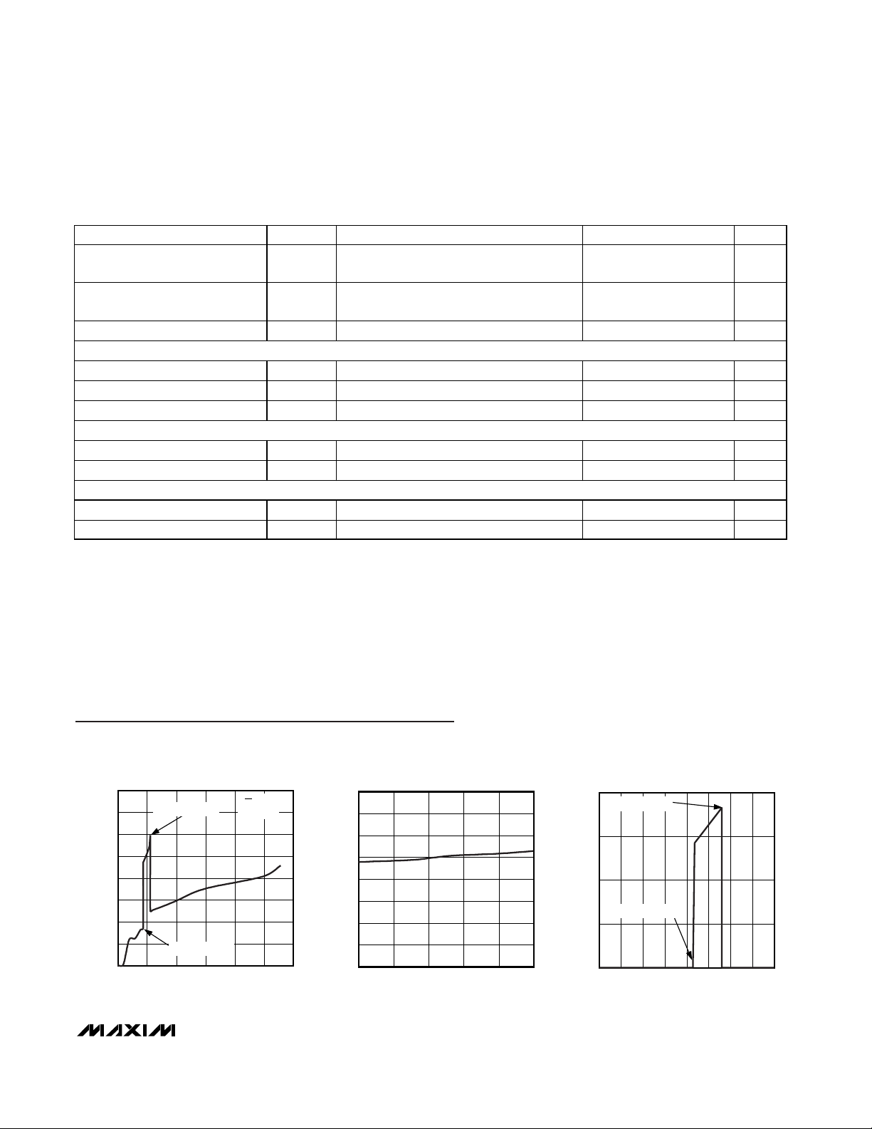
Typical Operating Characteristics
(VIN= 5V, TA= +25°C, otherwise noted.)
IIN + I
BTA
CURRENT vs. INPUT VOLTAGE
INPUT VOLTAGE (V)
I
IN
+ I
BTA
CURRENT (μA)
MAX4880 toc01
0 5 10 15 20 25 30
0
50
100
150
200
250
300
350
400
VEN = 0
V
CB
= 5V
OVLO TRIP POINT
UVLO TRIP POINT
IIN + I
BTA
CURRENT vs. TEMPERATURE
TEMPERATURE (°C)
I
IN
+ I
BTA
CURRENT (μA)
MAX4880 toc02
-40 -15 10 35 60 85
0
50
100
150
200
250
300
350
400
GATE VOLTAGE vs. INPUT VOLTAGE
INPUT VOLTAGE (V)
GATE VOLTAGE (V)
MAX4880 toc03
012345678
0
3
6
9
12
UVLO TRIP POINT
OVLO TRIP POINT
100
580
+150
Page 4

MAX4880
Overvoltage-Protection Controller with
Internal Disconnect Switch
4 _______________________________________________________________________________________
Typical Operating Characteristics (continued)
(VIN= 5V, TA= +25°C, otherwise noted.)
BTB TRIP LEVEL vs. INPUT VOLTAGE
INPUT VOLTAGE (V)
BTB TRIP LEVEL (V)
MAX4880 toc04
5.0 5.1 5.2 5.3 5.4 5.5 5.6 5.7
4.00
4.04
4.08
4.12
4.16
4.20
BTB TRIP LEVEL vs. TEMPERATURE
TEMPERATURE (°C)
BTB TRIP LEVEL (V)
MAX4880 toc05
-40 -15 10 35 60 85
4.00
4.04
4.08
4.12
4.16
4.20
BTB OFF CURRENT vs. TEMPERATURE
TEMPERATURE (°C)
BTB OFF CURRENT (nA)
MAX4880 toc06
-40 -15 10 35 60 85
0.1
1
10
100
1000
VEN = 0V
V
CB
= 0V
V
BTB
= 5.5V
POWER-UP RESPONSE
MAX4880 toc07
20ms/div
5V
0
10V
0
5V
0
5V
0
IN
GATE
BTA
FLAGV
POWER-DOWN RESPONSE
MAX4880 toc08
20ms/div
5V
0
10V
0
5V
0
5V
0
IN
GATE
BTA
FLAGV
EN vs. GATE
MAX4880 toc09
100μs/div
5V
0
10V
0
EN
GATE
OVERVOLTAGE RESPONSE
MAX4880 toc10
400ns/div
8V
5V
10V
0
50mA
0
5V
0
IN
GATE
I
GATE
FLAGV
Page 5

MAX4880
Overvoltage-Protection Controller with
Internal Disconnect Switch
_______________________________________________________________________________________ 5
CURRENT LIMIT vs. TEMPERATURE
TEMPERATURE (°C)
CURRENT LIMIT (mA)
MAX4880 toc11
-40 -15 10 35 60 85
0
100
200
300
400
500
600
700
800
VCB = 5V
V
BTA
= 5V
V
BTB
= 3.6V
CURRENT LIMIT vs. V
BTB
V
BTB
(V)
CURRENT LIMIT (mA)
MAX4880 toc12
1.0 1.5 2.0 2.5 3.0 3.5 4.0 4.5
0
100
200
300
400
500
600
700
800
VCB = 5V
V
BTA
= 5V
Pin Description
Typical Operating Characteristics (continued)
(VIN= 5V, TA = +25°C, otherwise noted.)
PIN NAME FUNCTION
1IN
Input. IN is the power input for the overvoltage (OVP) charge pump. Bypass IN to GND with a 1µF or
larger capacitor to achieve 15kV ESD protection.
2 EN
Active-Low Enable Input. Driving EN high turns off the external MOSFET. Pulling EN low activates the
overvoltage-protection circuitry and turns on the external MOSFET.
3 GATE
Gate-Drive Output. GATE is the output of an on-chip OVP charge pump. When V
UVLO
< VIN < V
OVLO
,
GATE is driven high to turn on the external n-channel MOSFET. When V
IN (MIN)
< VIN < V
UVLO
or VIN >
V
OVLO
, GATE is driven low to turn off the external n-channel MOSFET.
4 BTA
Input Terminal for the Internal-Current-Limited Switch. Connect BTA to the source of the external nchannel MOSFET. BTA is the power input for the entire device (except the OVP charge pump). Bypass
BTA to GND with a 0.1µF capacitor as close to the device as possible.
5CB
Control Input for the Internal-Current-Limited Switch. Drive CB high to leave the internal switch control for
the internal logic. The internal switch turns on and off depending on the battery voltage level. The internal
switch turns off when the battery voltage reaches the BTB trip level (4.2V), and turns back on when the
battery falls by 200mV. Driving CB low turns off the internal switch regardless of the battery voltage.
6 GND Ground
7 BTB
Output Terminal for the Internal-Current-Limited Switch. When the BTB voltage exceeds the trip level
(4.2V), the internal switch opens. The switch closes only when the BTB voltage drops 200mV below the
trip level.
8
Battery-Voltage-Sensing Input. BTB_SNS must be connected to BTB for proper operation. Bypass
BTB_SNS to GND with a 0.1µF capacitor as close to the device as possible.
9
Active-Low, Open-Drain, Battery-Voltage-Limit Flag Output. BAT_OK asserts low when the voltage on BTB
exceeds the BTB trip level (4.2V). BAT_OK is disabled when EN goes high.
BTB_SNS
BAT_OK
Page 6

MAX4880
Overvoltage-Protection Controller with
Internal Disconnect Switch
6 _______________________________________________________________________________________
Pin Description (continued)
PIN NAME FUNCTION
10
Active-Low, Open-Drain-Fault Flag Output. FLAGV goes low when either an overvoltage or undervoltage
fault occurs at IN. FLAGV is disabled when EN goes high. During startup, FLAGV has a delay of 50ms
after V
GATE
> 0.3V, before being initially driven high.
—EP
Exposed Pad. EP is internally connected to GND. Do not use EP as the only electrical ground connection.
Figure 1. Startup Timing Diagram
V
IN
V
GATE
V
OVLO
0.3V
t
GOFF
0.4V
t
FLAG
5V
8V
V
FLAGV
Figure 2. Overvoltage Fault Timing Diagram
V
IN
I
GATE
V
OVLO
80%
t
OVP
0V
Figure 3. Power-Up Overvoltage Timing Diagram
V
GATE
0.3V
t
DIS
2.4V
V
EN
Figure 4. Disable Timing Diagram
FLAGV
V
FLAGV
V
V
1.2V
GATE
IN
V
UVLO
t
START
t
GON
0.3V
5V
8V
t
DELAY
2.4V
Page 7

Detailed Description
The MAX4880 provides up to 28V overvoltage protection
for low-voltage systems. When the input voltage at IN
exceeds the overvoltage trip level (OVLO), the MAX4880
turns off a low-cost, external n-channel MOSFET to prevent damage to the protected components and issues
an overvoltage fault flag.
When the correct adapter is plugged in, the n-channel
MOSFET is turned on. The output of the MOSFET is
then connected to the internal current-limit switch that
provides the charge-current path to the battery. When
the battery reaches the trip voltage (4.2V), the internal
switch turns off and BAT_OK asserts low, indicating
that the battery has reached its full charged state. The
internal switch turns back on only when the battery voltage drops by more than 200mV.
IN Overvoltage Lockout (OVLO)
The MAX4880 has a 5.6V typical overvoltage threshold
(OVLO). When VINis higher than V
OVLO
, GATE goes
low to turn off the external n-channel MOSFET. An overvoltage FLAGV is asserted low to notify the processor
of the fault condition.
IN Undervoltage Lockout (UVLO)
The MAX4880 includes a fixed 4.35V typical undervoltage-lockout level (UVLO). When VINis below the V
UVLO
(1.2V ≤ VIN≤ 4.35V), GATE goes low to turn off the
external n-channel MOSFET. In addition, the driver for
the internal switch (BTA-BTB) is also turned off; therefore, this switch is open. This ensures the reverse current, drained from the battery, is less than 1µA when
the adapter is not present.
Fault Flag Output (
FLAGV
)
The FLAGV output signals the host system that there is
a fault with the input voltage. FLAGV asserts low in
response to either an overvoltage or an undervoltage
fault. FLAGV stays low for 50ms after GATE turns on,
before deasserting high.
FLAGV is an open-drain, active-low output. Connect a
pullup resistor from FLAGV to the logic I/O voltage of
the host system or to any voltage source up to 6V.
FLAGV is invalid when driving EN high.
Battery-Voltage-Limit Flag Output
(
BAT_OK
)
The MAX4880 includes a battery-voltage-limit flag output (BAT_OK). BAT_OK asserts low to indicate the voltage on BTB exceeds the BTB trip level of 4.2V.
BAT_OK deasserts high when the voltage on BTB falls
by the BTB hysteresis voltage of more than 200mV.
BAT_OK is an open-drain, active-low output. Connect a
pullup resistor from BAT_OK to the logic I/O voltage of
the host system, or to any voltage source up to 6V.
BAT_OK is invalid when driving EN high.
EN
Input
The MAX4880 features an active-low enable input (EN).
Drive EN low or connect to ground for normal operation. Drive EN high to force the external n-channel
MOSFET off, disabling FLAGV and BAT_OK.
Internal Current Limit (BTA to BTB)
The internal switch from BTA to BTB has a preset current-limit of 525mA (typ). If the load current from BTA to
BTB reaches this current limit, the switch operates in
the continuous mode, limiting the load current to the
preset value.
The switch remains in the current-limit condition until the
battery voltage on BTB exceeds 4.2V, or until the control
bit CB is driven low to open the switch.
Internal Switch Control Input (CB)
The CB input controls the internal switch. When CB is
high, the on/off state of the internal switch depends on
the battery voltage level. The internal switch turns off
when the battery voltage reaches the BTB trip level,
MAX4880
Overvoltage-Protection Controller with
Internal Disconnect Switch
_______________________________________________________________________________________ 7
IN
OVLO
UVLO
10V
CHARGE PUMP
GATE
IN
BAT_OK
FLAGV
EN
CHARGE
PUMP
GND
525mA
LIMIT
I
REF
V
REF
BTA
UVLO
BTA
BTB
BTB_SNS
CB
MAX4880
Figure 5. Functional Diagram
Page 8

MAX4880
and turns back on when the battery falls below the BTB
trip level minus BTB hysteresis. Drive CB low to turn off
the internal switch, regardless of the battery voltage.
This control bit can be used to provide additional topoff charge for the battery. When the CB pin is cycled,
the internal battery switch is turned on and off. This
effectively provides an average current that is lower
than the full-charge current.
GATE Driver
An on-chip charge pump drives the GATE voltage to
approximately twice VIN, allowing the use of a low-cost,
n-channel MOSFET (Figure 5). The actual GATE output
voltage tracks approximately 2 x V
IN,
until VINexceeds
the OVLO trip level, 5.6V (typ). The GATE output voltage, as a function of input voltage, is shown in the
Typical Operating Characteristics.
Applications Information
MOSFET Selection
The MAX4880 is designed for use with an n-channel
MOSFET. MOSFETs with R
DS(ON)
specified for a VGSof
4.5V are ideal. If the input supply is near the UVLO minimum of 4.2V, consider using a MOSFET specified for a
lower VGSvoltage. Also, the VDSshould be 30V for the
MOSFET to withstand the full 28V IN range of the
MAX4880. Table 1 shows a selection of MOSFETs
appropriate for use with the MAX4880.
IN Bypass Considerations
Bypass IN to GND with a 1µF ceramic capacitor to
achieve 15kV ESD-protected input. When the power
source has significant inductance due to long lead
length, take care to prevent overshoots due to the LC
Overvoltage-Protection Controller with
Internal Disconnect Switch
8 _______________________________________________________________________________________
CHARGE-CURRENT-
LIMIT RESISTOR
DISCHARGE
RESISTANCE
STORAGE
CAPACITOR
C
s
150pF
R
C
50Ω to 100Ω
RD
330Ω
HIGH-
VOLTAGE
DC
SOURCE
DEVICE
UNDER
TEST
Figure 8. IEC 61000-4-2 ESD Test Model
CHARGE-CURRENT-
LIMIT RESISTOR
DISCHARGE
RESISTANCE
STORAGE
CAPACITOR
C
s
100pF
R
C
1MΩ
R
D
1.5kΩ
HIGH-
VOLTAGE
DC
SOURCE
DEVICE
UNDER
TEST
Figure 6. Human-Body ESD Test Model
IP 100%
90%
36.8%
t
RL
TIME
t
DL
CURRENT WAVEFORM
PEAK-TO-PEAK RINGING
(NOT DRAWN TO SCALE)
I
r
10%
0
0
AMPERES
Figure 7. Human-Body-Model Current Waveform
tr = 0.7ns TO 1ns
30ns
60ns
t
100%
90%
10%
I
PEAK
I
Figure 9. IEC 61000-4-2 ESD Generator Current
Page 9

tank circuit and provide protection if necessary to prevent exceeding the 30V absolute maximum rating on IN.
The MAX4880 provides protection against voltage
faults up to 28V, but this does not include negative voltages. If negative voltages are a concern, connect a
Schottky diode from IN to GND to clamp negative input
voltages.
Exposed Pad
The MAX4880 provides an exposed pad on the bottom
of the package. This pad is internally connected to
GND. For the best thermal conductivity and higher
power dissipation, solder the exposed pad to the
ground plane. Do not use the ground-connected pad
as the only electrical ground connection or ground
return. Use GND (pin 6) as the primary electrical
ground connection.
ESD Test Conditions
ESD performance depends on a number of conditions.
The MAX4880 is specified for 15kV typical ESD resistance on IN when IN is bypassed to ground with a 1µF
low-ESR ceramic capacitor. Contact Maxim for a reliability report that documents test setup, methodology,
and results.
Human Body Model
Figure 6 shows the Human Body Model, and Figure 7
shows the current waveform it generates when discharged into a low impedance. This model consists of
a 100pF capacitor charged to the ESD voltage of interest, which is then discharged into the device through a
1.5kΩ resistor.
IEC 61000-4-2
Since January 1996, all equipment manufactured and/or
sold in the European community has been required to
meet the stringent IEC 61000-4-2 specification. The IEC
61000-4-2 standard covers ESD testing and performance of finished equipment; it does not specifically
refer to integrated circuits. The MAX4880 helps users
design equipment that meets Level 3 of IEC 61000-4-2,
without additional ESD-protection components.
The main difference between tests done using the
Human Body Model and IEC 61000-4-2 is higher peak
current in IEC 61000-4-2. Because series resistance is
lower in the IEC 61000-4-2 ESD test model (Figure 8),
the ESD-withstand voltage measured to this standard is
generally lower than that measured using the Human
Body Model. Figure 9 shows the current waveform for
the ±8kV IEC 61000-4-2 Level 4 ESD ContactDischarge test. The Air-Gap test involves approaching
the device with a charger probe. The ContactDischarge method connects the probe to the device
before the probe is energized.
Chip Information
TRANSISTOR COUNT: 2391
PROCESS: BiCMOS
MAX4880
Overvoltage-Protection Controller with
Internal Disconnect Switch
_______________________________________________________________________________________ 9
PART
PACKAGE
V
DS
MAX (V)
R
ON
MANUFACTURER
Si1426DH Single/SC70-6 30 115
Vishay Siliconix
www.vishay.com
402-563-6866
FDG315N Single/SC70-6 30 160
Fairchild Semiconductor
www.fairchildsemi.com
207-775-8100
Table 1. MOSFET Suggestions
CONFIGURATION/
AT 4.5V (mΩ)
Page 10

MAX4880
Overvoltage-Protection Controller with
Internal Disconnect Switch
Maxim cannot assume responsibility for use of any circuitry other than circuitry entirely embodied in a Maxim product. No circuit patent licenses are
implied. Maxim reserves the right to change the circuitry and specifications without notice at any time.
10 ____________________Maxim Integrated Products, 120 San Gabriel Drive, Sunnyvale, CA 94086 408-737-7600
© 2005 Maxim Integrated Products Printed USA is a registered trademark of Maxim Integrated Products, Inc.
Jackson
Package Information
(The package drawing(s) in this data sheet may not reflect the most current specifications. For the latest package outline information
go to www.maxim-ic.com/packages
.)
Maxim cannot assume responsibility for use of any circuitry other than circuitry entirely embodied in a Maxim product. No circuit patent licenses are
implied. Maxim reserves the right to change the circuitry and specifications without notice at any time.
10 ____________________Maxim Integrated Products, 120 San Gabriel Drive, Sunnyvale, CA 94086 408-737-7600
© 2005 Maxim Integrated Products Printed USA is a registered trademark of Maxim Integrated Products. Inc.
6, 8, &10L, DFN THIN.EPS
L
C
L
C
PIN 1
INDEX
AREA
D
E
L
e
L
A
e
E2
N
G
1
2
21-0137
PACKAGE OUTLINE, 6,8,10 & 14L,
TDFN, EXPOSED PAD, 3x3x0.80 mm
-DRAWING NOT TO SCALE-
k
e
[(N/2)-1] x e
REF.
PIN 1 ID
0.35x0.35
DETAIL A
b
D2
A2
A1
COMMON DIMENSIONS
SYMBOL
MIN. MAX.
A
0.70 0.80
D
2.90 3.10
E 2.90 3.10
A1
0.00 0.05
L 0.20 0.40
PKG. CODE
N
D2 E2 e
JEDEC SPEC
b
[(N/2)-1] x e
PACKAGE VARIATIONS
0.25 MIN.k
A2 0.20 REF.
2.30±0.101.50±0.106T633-1 0.95 BSC MO229 / WEEA 1.90 REF0.40±0.05
1.95 REF0.30±0.05
0.65 BSC
2.30±0.108T833-1
2.00 REF0.25±0.05
0.50 BSC
2.30±0.1010T1033-1
2.40 REF0.20±0.05- - - -
0.40 BSC
1.70±0.10 2.30±0.1014T1433-1
1.50±0.10
1.50±0.10
MO229 / WEEC
MO229 / WEED-3
0.40 BSC
- - - - 0.20±0.05 2.40 REFT1433-2 14 2.30±0.101.70±0.10
T633-2 6 1.50±0.10 2.30±0.10 0.95 BSC
MO229 / WEEA
0.40±0.05 1.90 REF
T833-2 8 1.50±0.10 2.30±0.10
0.65 BSC MO229 / WEEC
0.30±0.05 1.95 REF
T833-3 8 1.50±0.10 2.30±0.10
0.65 BSC MO229 / WEEC
0.30±0.05 1.95 REF
-DRAWING NOT TO SCALE-
G
2
2
21-0137
PACKAGE OUTLINE, 6,8,10 & 14L,
TDFN, EXPOSED PAD, 3x3x0.80 mm
DOWNBONDS
ALLOWED
NO
NO
NO
NO
YES
NO
YES
NO
 Loading...