

Page 1
For free samples & the latest literature: http://www.maxim-ic.com, or phone 1-800-998-8800.
For small orders, phone 408-737-7600 ext. 3468.
General Description
The MAX480 is a precision micropower operational amplifier with flexible power-supply capability. Its guaranteed
140µV maximum offset voltage (25µV typ) is the lowest of
any micropower op amp. Similarly, input bias current,
input offset current, and drift specifications are within tight
limits.
Both the input and output voltage ranges include the negative supply rail, allowing maximum signal range capability in single-supply applications. The MAX480 operates
with either a single supply ranging from +1.6V to +36V or
dual supplies from ±0.8V to ±18V. The MAX480 consumes less than 20µA, allowing operation in excess of
10,000 hours from a 250mA-hr lithium coin cell. Even with
a minimal quiescent current, the amplifier sinks or sources
5mA from its output.
The MAX480 is available in 8-pin DIP and SO packages in
commercial, extended, and military temperature ranges.
Applications
Precision Micropower Amplifiers
Micropower Signal Processing
Battery-Powered Analog Circuits
Features
♦ Single- or Dual-Supply Operation: +1.6V to +36V,
±0.8V to ±18V
♦ True Single-Supply Operation: Input and Output
Voltage Ranges Include Ground
♦ 2.0µV/°C Max Offset Voltage Drift
♦ 20µA Max Supply Current
♦ 5mA Min Output Drive
♦ 140µV Max Input Offset Voltage
♦ 3nA Max Input Bias Current
♦ 500V/mV Min Open-Loop Gain
♦ Standard 741 Pinout with Nulling to V-
MAX480
High-Precision, Low-Voltage,
Micropower Op Amp
________________________________________________________________
Maxim Integrated Products
1
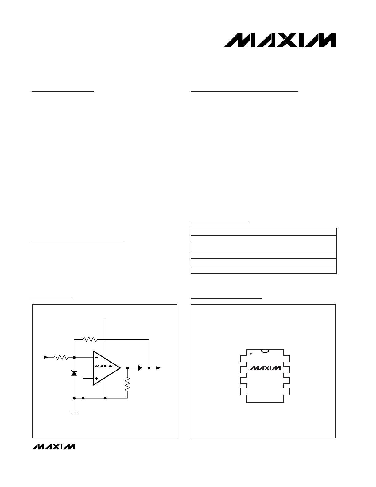
MAX480
OUT
V
IN
HP5082-2800
IN914
6
7
4
2
3
V+ (5V)
R2
10k
R1
10k
R3
100k
SINGLE OP AMP FULL-WAVE RECTIFIER
Typical Operating Circuit
19-2772; Rev 3a; 1/98
PART
MAX480CPA
MAX480CSA 0°C to +70°C
0°C to +70°C
TEMP. RANGE PIN-PACKAGE
8 Plastic DIP
8 SO
Pin Configuration
Ordering Information
MAX480EPA
MAX480ESA -40°C to +85°C
-40°C to +85°C 8 Plastic DIP
8 SO
MAX480MJA -55°C to +125°C 8 CERDIP
OUT
NULLV-
1
2
87N.C.
V+IN-
IN+
NULL
DIP/SO
TOP VIEW
3
4
6
5
MAX480
Page 2
MAX480
High-Precision, Low-Voltage,
Micropower Op Amp
2 _______________________________________________________________________________________
ABSOLUTE MAXIMUM RATINGS
ELECTRICAL CHARACTERISTICS
(VS= ±1.5V to ±15V, TA= +25°C, unless otherwise noted.)
Stresses beyond those listed under “Absolute Maximum Ratings” may cause permanent damage to the device. These are stress ratings only, and functional
operation of the device at these or any other conditions beyond those indicated in the operational sections of the specifications is not implied. Exposure to
absolute maximum rating conditions for extended periods may affect device reliability.
Supply Voltage (V+ to V-)....................................................±18V
Differential Input Voltage........................(V- - 20V) to (V+ + 20V)
Common-Mode Input Voltage ................(V- - 20V) to (V+ + 20V)
Output Short-Circuit Duration........................................Indefinite
Continuous Power Dissipation
Plastic DIP (derate 9.09mW/°C above +70°C) .............727mW
SO (derate 5.88mW/°C above +70°C)..............................471mW
CERDIP (derate 8.0mW/°C above +70°C)....................640mW
Operating Temperature Ranges
MAX480C_A.........................................................0°C to +70°C
MAX480E_A......................................................-40°C to +85°C
MAX480MJA...................................................-55°C to +125°C
Junction Temperature (T
J
).................................-65°C to +150°C
Storage Temperature Range.............................-65°C to +150°C
Lead Temperature (soldering, 10sec).............................+300°C
f
O
= 0.1Hz to 10Hz, VS= ±15V
AV= +1V/V, no oscillations (Note 2)
VCM= 0
VS= ±15V
VCM= 0
V+ = 5V, V- = 0, RL= 10kΩ
V+ = 5V, V- = 0, RL= 2kΩ
V+ = 5V, V- = 0
VS= ±15V
VS= ±15V,
VO= ±10V
CONDITIONS
µVp-p3e
np-p
Input Noise Voltage
pF250 650Capacitive Load Stability
µA
915
I
SY
Supply Current
V/ms512SRSlew Rate
µV/V1.0 12PSRRPower-Supply Rejection Ratio
V
100 500
V
O
4.0 4.2
±14 ±14.2
V
0/4
IVRInput Voltage
nA13I
B
Input Bias Current
nA0.2 1I
OS
µV25 140V
OS
Input Offset Voltage
Input Offset Current
V/mV
500 1200
UNITSMIN TYP MAXSYMBOLPARAMETER
VS= ±15V
VS= ±15V
GΩ20R
INCM
Common-Mode Input Resistance
MΩ30R
IN
Differential-Mode Input Resistance
V
OL
V
OH
Output Voltage Swing
V+ = 5V, V- = 0, 0 < VCM< 4V
dB
85 110
CMRRCommon-Mode Rejection Ratio
VS= ±1.5V
µV
RL= 100kΩ
RL= 2kΩ
RL= 10kΩ
75 250
200 600
RL= 100kΩ
V+ = 5V, V- = 0,
1V < VO< 4V
RL= 10kΩ
A
VO
Large-Signal Voltage Gain
50 180
100 400
VS= ±15kV (Note 1) -15/13.5
RL= 10kΩ
RL= 2kΩ ±11 ±12
VS= ±15V, -15V < VCM< 13.5V 90 130
VS= ±15V 14 20
Page 3

MAX480
High-Precision, Low-Voltage,
Micropower Op Amp
_______________________________________________________________________________________ 3
ELECTRICAL CHARACTERISTICS
(VS= ±1.5V to ±15V, TA= T
MIN
to T
MAX
, unless otherwise noted.)
VCM= 0
VS= ±1.5V
(Note 2)
VS= ±15V
CONDITIONS
µA
12 25
I
SY
Supply Current
µV/V1.0 12PSRR
Power-Supply
Rejection Ratio
V
O
±13.5 ±14
nA0.2 2.0I
OS
Input Offset
Current
µV/°C0.3 2.0TCV
OS
µV40 220V
OS
Input Offset
Voltage
Input Offset
Voltage Drift
A
VO
Large-Signal
Voltage Gain
350 950
UNITS
MAX480C
MIN TYP MAX
SYMBOLPARAMETER
Note 1: Guaranteed by CMRR test.
Note 2: Guaranteed by design.
VCM= 0 nA13I
B
Input Bias
Current
V+ = 5V, V- = 0
V
0/3.5
IVR
Input Voltage
Range
25
13 25
1.0 12
0/3.5
±13.5 ±14
0.3 2.0
0.3 2.0
50 250
350 800
MAX480E
MIN TYP MAX
37
15 25
3.2 15
0/3.5
±13.5 ±13.7
0.5 2.0
0.3 2.0
70 300
60 400
MAX480M
MIN TYP MAX
V+ = 5V, V- = 0
RL= 2kΩ
3.9 4.1V
OH
3.9 4.1 3.9 4.1
V+ = 5V, V- = 0
RL= 10kΩ
100 500V
OL
µV100 500 100 500
85 110
V+ = 5V, V- = 0,
0 < V
CM
< 3.5V
85 110 80 105
VS= ±15V,
V = ±10V
RL= 100kΩ
RL= 10kΩ
RL= 2kΩ 55 125
130 400
55 150
130 400
30 110
45 240
V+ = 5V,
V- = 0,
1V < VO< 4V
30 150
RL= 100kΩ
RL= 10kΩ 30 140 22 110
50 280
V/mV
50 360 35 200
VS= ±15V (Note 1) -15/13.5 -15/13.5 -15/13.5
RL= 10kΩ
RL= 2kΩ
Output Voltage
Swing
V
±10.5 ±11.8 ±10.5 ±11.8 ±10.5 ±11.5
VS= ±15V,
-15V < V
CM
< 13.5V
CMRR
Common-Mode
Rejection Ratio
90 120 90 120 85 115
dB
VS= ±15V 16 30 17 30 19 30
Page 4

MAX480
High-Precision, Low-Voltage,
Micropower Op Amp
4 _______________________________________________________________________________________
Typical Operating Characteristics
(TA = +25°C, unless otherwise noted.)
0
20
60
40
80
100
-75 -25 0-50 25 50 75 100 125
INPUT OFFSET VOLTAGE
vs. TEMPERATURE
MAX480-01
TEMPERATURE (°C)
INPUT OFFSET VOLTAGE (µV)
VS = ±15V
0
0.2
1.0
0.8
0.6
0.4
1.2
1.4
-75 -25 0-50 25 50 75 100 125
INPUT OFFSET CURRENT
vs. TEMPERATURE
MAX480-02
TEMPERATURE (°C)
INPUT OFFSET CURRENT (nA)
VS = ±15V
0
0.2
0.8
0.6
0.4
1.0
1.2
-75 -25 0-50 25 50 75 100 125
INPUT BIAS CURRENT
vs. TEMPERATURE
MAX480-03
TEMPERATURE (°C)
INPUT BIAS CURRENT (nA)
VS = ±15V
2
6
4
16
14
12
10
8
18
20
22
-75 -25 0-50 25 50 75 100 125
SUPPLY CURRENT
vs. TEMPERATURE
MAX480-04
TEMPERATURE (°C)
SUPPLY CURRENT (µA)
VS = ±15V
VS = ±1.5V
NO LOAD
60
-20
10 1k 10k100 100k
CLOSED-LOOP GAIN
vs. FREQUENCY
MAX480-07
FREQUENCY (Hz)
CLOSED-LOOP GAIN (dB)
0
20
40
VS = ±15V
0
200
100
400
300
500
600
010155 202530
OPEN-LOOP GAIN vs.
SINGLE-SUPPLY VOLTAGE
MAX480-05
SINGLE-SUPPLY VOLTAGE (V)
OPEN-LOOP GAIN (V/mV)
RL = 10kΩ
TA = +25°C
TA = +85°C
TA = +125°C
0
40
20
100
80
60
120
140
0.1 10 1001 1k 10k 100k
OPEN-LOOP GAIN AND
PHASE SHIFT vs. FREQUENCY
MAX480-06
FREQUENCY (Hz)
OPEN-LOOP GAIN (dB)
GAIN
PHASE
VS = ±15V
R
L
= 100kΩ
135
180
0
45
90
PHASE SHIFT (DEGREES)
0
100 100k10k1k
OUTPUT VOLTAGE SWING
vs. LOAD RESISTANCE
2
3
6
1
5
4
MAX480-08
LOAD RESISTANCE (Ω)
OUTPUT VOLTAGE SWING (V)
V+ = 5V
V- = 0
0
100 100k10k1k
OUTPUT VOLTAGE SWING
vs. LOAD RESISTANCE
4
6
8
16
2
14
12
10
MAX480-09
LOAD RESISTANCE (Ω)
OUTPUT VOLTAGE SWING (V)
VS = ±15V
POSITIVE SUPPLY
NEGATIVE SUPPLY
Page 5

MAX480
High-Precision, Low-Voltage,
Micropower Op Amp
_______________________________________________________________________________________
5
20
11k10010
POWER-SUPPLY REJECTION
RATIO vs. FREQUENCY
60
120
40
100
80
MAX480-10
FREQUENCY (Hz)
POWER-SUPPLY REJECTION (dB)
POSITIVE SUPPLY
NEGATIVE SUPPLY
40
11k10010
COMMON-MODE REJECTION
RATIO vs. FREQUENCY
80
140
60
120
100
MAX480-11
FREQUENCY (Hz)
COMMON-MODE REJECTION (dB)
VS = ± 15V
1000
1
0.1 10 10011k
NOISE VOLTAGE DENSITY
vs. FREQUENCY
MAX480-12
FREQUENCY (Hz)
NOISE VOLTAGE DENSITY (nV/√Hz)
10
100
VS = ±15V
100
0.1
0.1 10 10011k
CURRENT NOISE DENSITY
vs. FREQUENCY
MAX480-13
FREQUENCY (Hz)
CURRENT NOISE DENSITY (pA/√Hz)
1
10
VS = ±15V
VS = ±15V, AV = +1,
R
L
= 10kΩ, CL = 500pF
100µs/div
SMALL-SIGNAL
TRANSIENT RESPONSE
MAX480-14
VS = ±15V, AV = +1,
R
L
= 10kΩ, CL = 500pF
LARGE-SIGNAL
TRANSIENT RESPONSE
MAX480-15
1ms/div
Typical Operating Characteristics (continued)
(TA = +25°C, unless otherwise noted.)
Page 6

MAX480
High-Precision, Low-Voltage,
Micropower Op Amp
Maxim cannot assume responsibility for use of any circuitry other than circuitry entirely embodied in a Maxim product. No circuit patent licenses are
implied. Maxim reserves the right to change the circuitry and specifications without notice at any time.
6
_____________________Maxim Integrated Products, 120 San Gabriel Drive, Sunnyvale, CA 94086 408-737-7600
© 1998 Maxim Integrated Products Printed USA is a registered trademark of Maxim Integrated Products.
Package Information
IN-
OUT
V-
7
6
4
5
100k
V+
2
3
1
IN+
MAX480
Figure 1. Offset Nulling Circuit
MAX480
6
4
7
2
3
+15V
-15V
Figure 2. Burn-In Circuit
SOICN.EPS
 Loading...