

Page 1
19-6000; Rev 0; 10/11
MAX44251/MAX44252
20V, Ultra-Precision, Low-Noise Op Amps
General Description
The MAX44251/MAX44252 are 20V, ultra-precision, lownoise, low-drift amplifiers that offer near-zero DC offset
and drift through the use of patented autocorrelating
zeroing techniques. This method constantly measures
and compensates the input offset, eliminating drift over
time and temperature and the effect of 1/f noise. These
dual and quad devices feature rail-to-rail outputs, operate from a single 2.7V to 20V supply, and consume only
1.15mA per channel, while providing 5.9nV/√Hz inputreferred voltage noise. The ICs are unity-gain stable with
a gain-bandwidth product of 10MHz.
With excellent specifications such as offset voltage of
6µV (max), drift of 19nV/°C (max), and 123nV
0.1Hz to 10Hz, the ICs are ideally suited for applications
requiring ultra-low noise and DC precision such as interfacing with pressure sensors, strain gauges, precision
weight scales, and medical instrumentation.
The ICs are available in 8-pin SOT23, 8-pin µMAXM,
and 14-pin SOIC packages and are rated over the
-40°C to +125°C temperature range.
Ordering Information appears at end of data sheet.
Functional Diagrams appear at end of data sheet.
For related parts and recommended products to use with this part,
refer to www.maxim-ic.com/MAX44251.related.
noise in
P-P
Benefits and Features
S 2.7V to 20V Power-Supply Range
S Integrated EMI Filter
S 6µV Input Offset Voltage (max) at Room
Temperature
S TCVOS of 19nV/°C (max)
S Low 5.9nV/√Hz Input-Referred Voltage Noise
S 123nV
in 0.1Hz to 10Hz
P-P
S Fast 400ns Settling Time
S 10MHz Gain-Bandwidth Product
S Rail-to-Rail Output
S High Accuracy Enables Precision Signal Chain
Acquisition
Applications
Strain Gauges
Pressure Transducers
Medical Instrumentation
Precision Instrumentation
Load Cell and Bridge Transducer Amplification
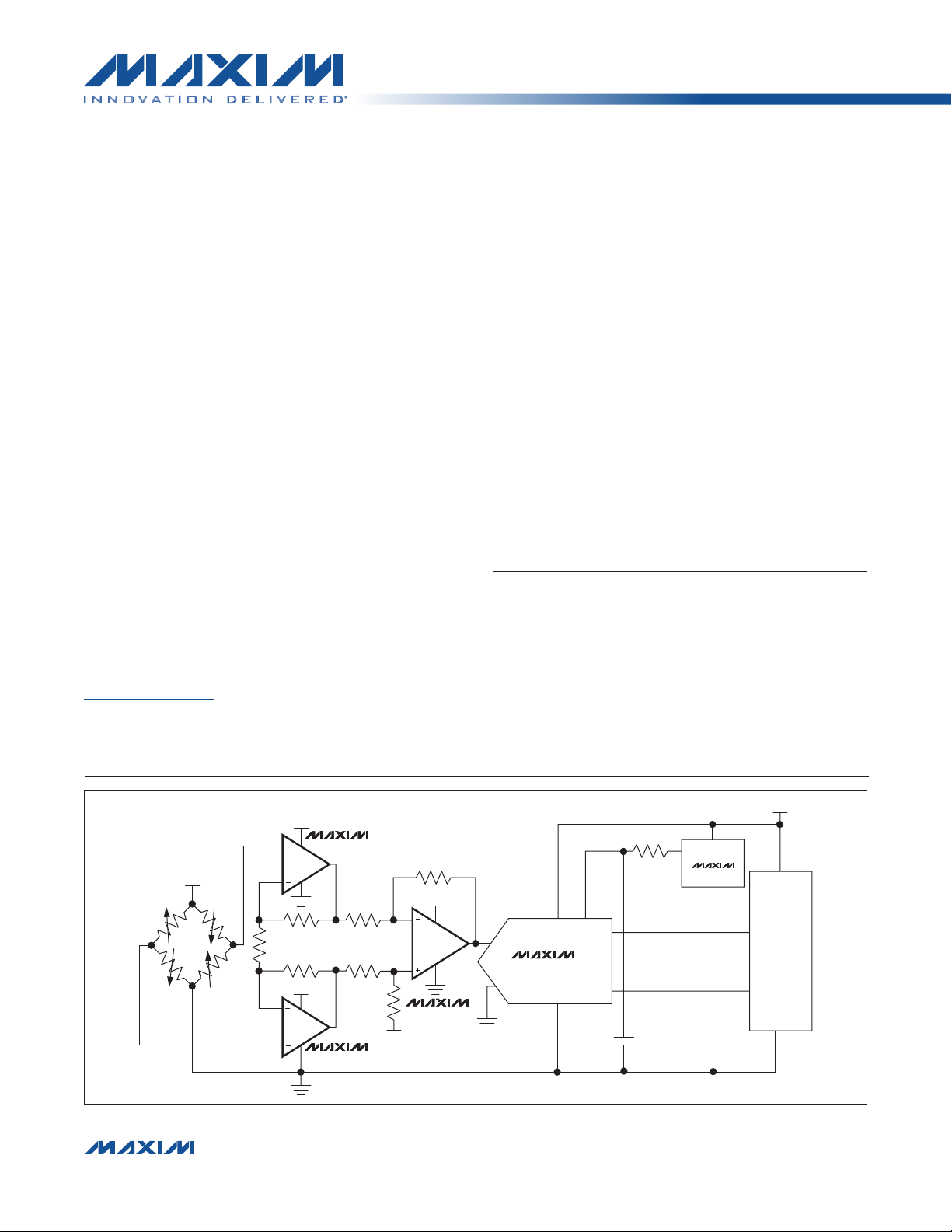
Typical Operating Circuit
3.3V
20V
MAX44251
1.5V
R
20V
BUFFER
MAX44251
V
IN+
V
IN-
V
DD
MAX11211
V
SS
V
REF
OUTPUT
20V
R
G
BUFFER
50R
50R
20V
BUFFER
G
G
MAX44251
R
R
R
µMAX is a registered trademark of Maxim Integrated Products, Inc.
����������������������������������������������������������������� Maxim Integrated Products 1
For pricing, delivery, and ordering information, please contact Maxim Direct at 1-888-629-4642,
or visit Maxim’s website at www.maxim-ic.com.
3V
V
R
C
1
OUT
1
MAX6126
V
DD
MICRO-
PROCESSOR
Page 2
MAX44251/MAX44252
20V, Ultra-Precision, Low-Noise Op Amps
ABSOLUTE MAXIMUM RATINGS
Supply Voltage (VDD to VSS).................................-0.3V to +22V
All Other Pins ..................................(VSS - 0.3V) to (VDD + 0.3V)
Short-Circuit Duration to Either Supply Rail ............................ 1s
Continuous Input Current (any pin) ................................. ±20mA
Differential Input Voltage ...................................................... ±6V
Maximum Power Dissipation (TA = +70°C)
SOT23 (derate 9.1 mW/°C above +70°C) ...................727mW
µMAX (derate 4.5 mW/°C above +70°C) ....................362mW
SOIC (derate 8.3 mW/°C above +70°C) ..................666.7mW
Stresses beyond those listed under “Absolute Maximum Ratings” may cause permanent damage to the device. These are stress ratings only, and functional operation of the device at these or any other conditions beyond those indicated in the operational sections of the specifications is not implied. Exposure to absolute
maximum rating conditions for extended periods may affect device reliability.
PACKAGE THERMAL CHARACTERISTICS (Note 1)
SOT23
Junction-to-Ambient Thermal Resistance (ΘJA) ....... 196°C/W
Junction-to-Case Thermal Resistance (ΘJC) ...............70°C/W
µMAX
Junction-to-Ambient Thermal Resistance (ΘJA) ........221°C/W
Junction-to-Case Thermal Resistance (ΘJC) ...............42°C/W
Operating Temperature Range ........................ -40°C to +125NC
Junction Temperature .....................................................+150NC
Storage Temperature Range ............................ -65°C to +150NC
Lead Temperature (soldering, 10s) .............................. +300NC
Soldering Temperature (reflow) .................................... +260NC
SOIC
Junction-to-Ambient Thermal Resistance (ΘJA) ........120°C/W
Junction-to-Case Thermal Resistance (ΘJC) ...............37°C/W
Note 1: Package thermal resistances were obtained using the method described in JEDEC specification JESD51-7, using a four-
layer board. For detailed information on package thermal considerations, refer to www.maxim-ic.com/thermal-tutorial.
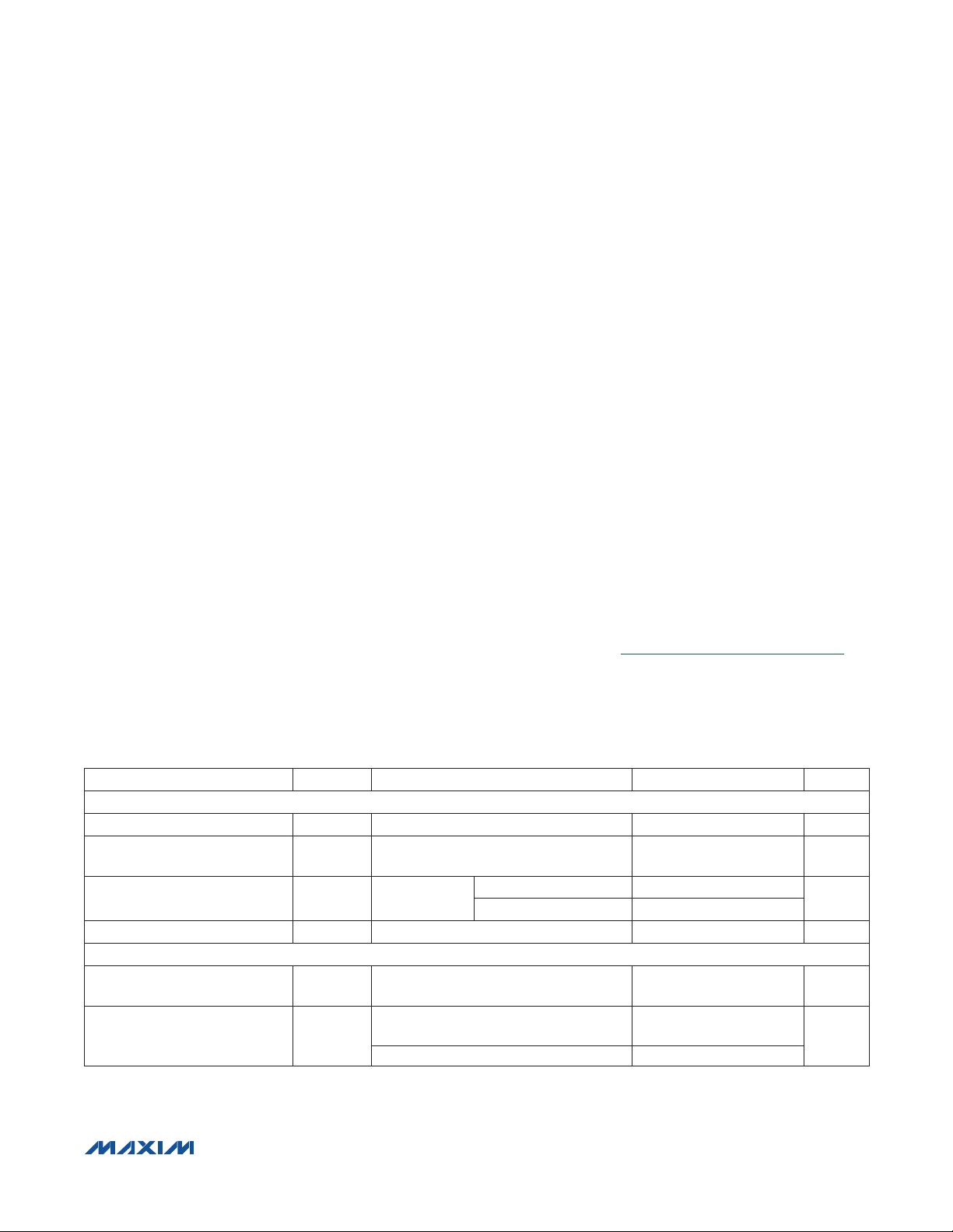
ELECTRICAL CHARACTERISTICS
(VDD = 10V, VSS = 0V, V
at +25°C.) (Note 2)
PARAMETER SYMBOL CONDITIONS MIN TYP MAX UNITS
POWER SUPPLY
Supply Voltage Range V
Power-Supply Rejection Ratio
(Note 3)
Quiescent Current per Amplifier I
Power-Up Time t
DC SPECIFICATIONS
Input Common-Mode Range V
Common-Mode Rejection Ratio
(Note 3)
IN+
= V
= VDD/2, RL = 10kI to VDD/2, TA = -40°C to +125°C, unless otherwise noted. Typical values are
IN-
DD
PSRR VDD = 2.7V to 20V, VCM = 0V 140 145 dB
DD
ON
CM
CMRR
Guaranteed by PSRR 2.7 20 V
RL = J
Guaranteed by CMRR test
TA = +25NC, VCM = -0.05V to (VDD -
1.5V)
-40NC < TA < +125NC
TA = +25NC
-40NC < TA < +125NC
VSS -
0.05
133 140
130
1.15 1.55
1.75
25
VDD -
1.5
mA
Fs
V
dB
����������������������������������������������������������������� Maxim Integrated Products 2
Page 3
MAX44251/MAX44252
20V, Ultra-Precision, Low-Noise Op Amps
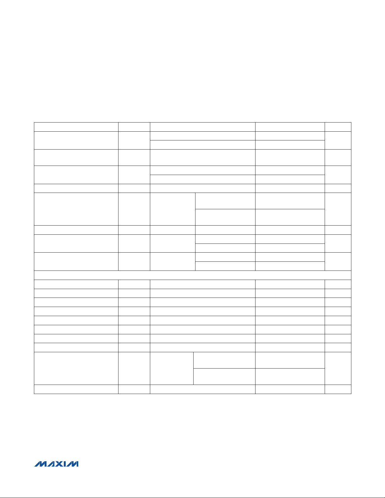
ELECTRICAL CHARACTERISTICS (continued)
(VDD = 10V, VSS = 0V, V
at +25°C.) (Note 2)
PARAMETER SYMBOL CONDITIONS MIN TYP MAX UNITS
Input Offset Voltage (Note 3) V
Input Offset Voltage Drift
(Note 3)
Input Bias Current (Note 3) I
Input Offset Current (Note 3) I
Open-Loop Gain (Note 3) A
Output Short-Circuit Current To VDD or V
Output Voltage Low V
Output Voltage High V
AC SPECIFICATIONS
Input Voltage-Noise Density e
Input Voltage Noise 0.1Hz < f < 10Hz 123 nV
Input Current-Noise Density i
Input Capacitance C
Gain-Bandwidth Product GBW 10 MHz
Phase Margin PM CL = 20pF 60 Degrees
Slew Rate SR AV = 1V/V, V
Capacitive Loading C
Total Harmonic Distortion THD
Settling Time To 0.01%, V
IN+
= V
= VDD/2, RL = 10kI to VDD/2, TA = -40°C to +125°C, unless otherwise noted. Typical values are
IN-
3 6
7
5 19
200 1300
2400
400 pA
12 25
45 85
18 37
71 135
2 pF
8
TC V
OS
VOL
OS
B
OL
OH
N
N
IN
L
TA = +25NC
-40NC < TA < +125NC
OS
TA = +25NC
-40NC < TA < +125NC
250mV P V
P VDD - 250mV,
RL = 10kI to
VDD/2
V
- V
OUT
VDD - V
SS
OUT
OUT
SS
TA = +25NC
-40NC < TA < +125NC
145 154
136
Noncontinuous 96 mA
RL = 10kI to VDD/2
RL = 2kI to VDD/2
RL = 10kI to VDD/2
RL = 2kI to VDD/2
f = 1kHz 5.9
f = 1kHz 0.6
= 2V
OUT
P-P
No sustained oscillation, AV = 1V/V 500 pF
V
= 2V
OUT
AV = +1V/V,
RL = 10kI to
VDD/2
,
P-P
f = 1kHz -124
f = 20kHz -119
= 2V step, AV = -1V/V 400 ns
OUT
nV/NC
mV
mV
nV/√Hz
pA/√Hz
V/Fs
FV
pA
dB
P-P
dB
����������������������������������������������������������������� Maxim Integrated Products 3
Page 4
MAX44251/MAX44252
20V, Ultra-Precision, Low-Noise Op Amps
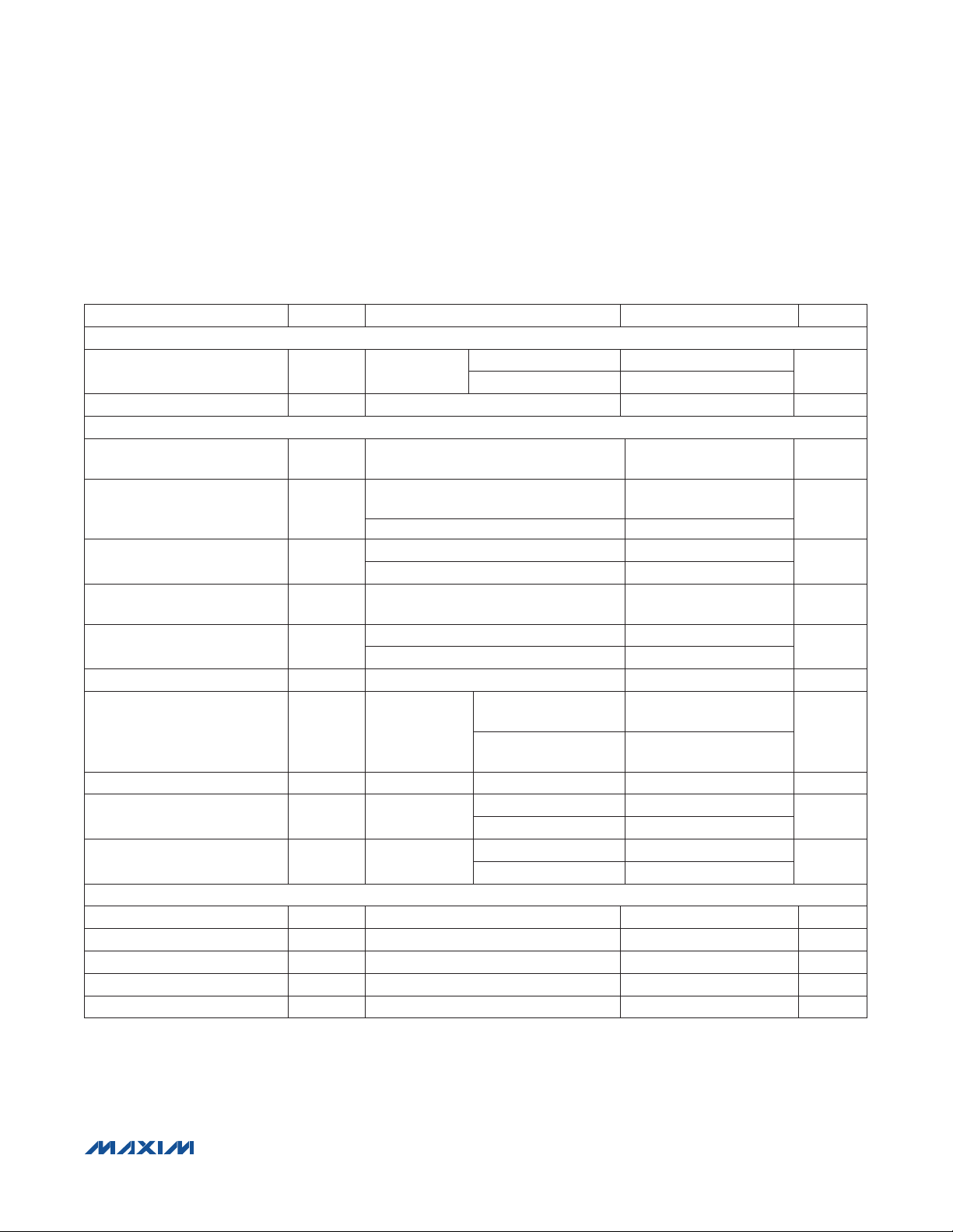
ELECTRICAL CHARACTERISTICS
(VDD = 3.3V, VSS = 0V, V
are at +25°C.) (Note 2)
PARAMETER SYMBOL CONDITIONS MIN TYP MAX UNITS
POWER SUPPLY
Quiescent Current per Amplifier I
Power-Up Time t
DC SPECIFICATIONS
Input Common-Mode Range V
Common-Mode Rejection Ratio
(Note 3)
Input Offset Voltage (Note 3) V
Input Offset Voltage Drift
(Note 3)
Input Bias Current (Note 3) I
Input Offset Current (Note 3) I
Open-Loop Gain (Note 3) A
Output Short-Circuit Current To VDD or V
Output Voltage Low V
Output Voltage High V
AC SPECIFICATIONS
Input Voltage-Noise Density e
Input Voltage Noise 0.1Hz < f < 10Hz 123 nV
Input Current-Noise Density i
Input Capacitance C
Gain-Bandwidth Product GBW 10 MHz
IN+
= V
= VDD/2, RL = 10kI to VDD/2, TA = -40°C to +125°C, unless otherwise noted. Typical values
IN-
DD
ON
CM
CMRR
OS
TC V
B
OS
VOL
OL
OH
N
N
IN
RL = J
Guaranteed by CMRR test
TA = +25NC, VCM = -0.05V to (VDD -
1.5V)
-40NC < TA < +125NC
TA = +25NC
-40NC < TA < +125NC
OS
TA = +25NC
-40NC < TA < +125NC
250mV P V
P VDD - 250mV,
RL = 10kI to
VDD/2
V
- V
OUT
SS
VDD - V
OUT
f = 1kHz 6.2
f = 1kHz 0.3
TA = +25NC
-40NC < TA < +125NC
OUT
TA = +25NC
-40NC < TA < +125NC
Noncontinuous 58 mA
SS
RL = 10kI to VDD/2
RL = 2kI to VDD/2
RL = 10kI to VDD/2
RL = 2kI to VDD/2
VSS -
0.05
120 129
117
136 151
133
1.1 1.5
1.65
25
VDD -
1.5
3 5.5
6.5
8 18
200 1100
1200
400 pA
5 22
17 42
9 22
29 52
2 pF
nV/NC
nV/√Hz
pA/√Hz
mA
Fs
V
dB
FV
pA
dB
mV
mV
P-P
����������������������������������������������������������������� Maxim Integrated Products 4
Page 5
MAX44251/MAX44252
02
20V, Ultra-Precision, Low-Noise Op Amps
ELECTRICAL CHARACTERISTICS (continued)
(VDD = 3.3V, VSS = 0V, V
at +25°C.) (Note 2)
PARAMETER SYMBOL CONDITIONS MIN TYP MAX UNITS
Phase Margin PM CL = 20pF 60 Degrees
Slew Rate SR AV = 1V/V, V
Capacitive Loading C
Total Harmonic Distortion THD
IN+
= V
= VDD/2, RL = 10kI to VDD/2, TA = -40°C to +125°C, unless otherwise noted. Typical values are
IN-
= 1V
OUT
No sustained oscillation, AV = 1V/V 500 pF
L
V
OUT
= 1V
P-P
,
AV = +1V/V,
, 10% to 90% 5
P-P
f = 1kHz -124
VCM = VDD/4,
RL = 10kI to
VDD/2
f = 20kHz -100
V/Fs
dB
Settling Time To 0.01%, V
= 1V step, AV = -1V/V 200 ns
OUT
Note 2: All devices are 100% production tested at TA = +25°C. Temperature limits are guaranteed by design.
Note 3: Guaranteed by design.
Typical Operating Characteristics
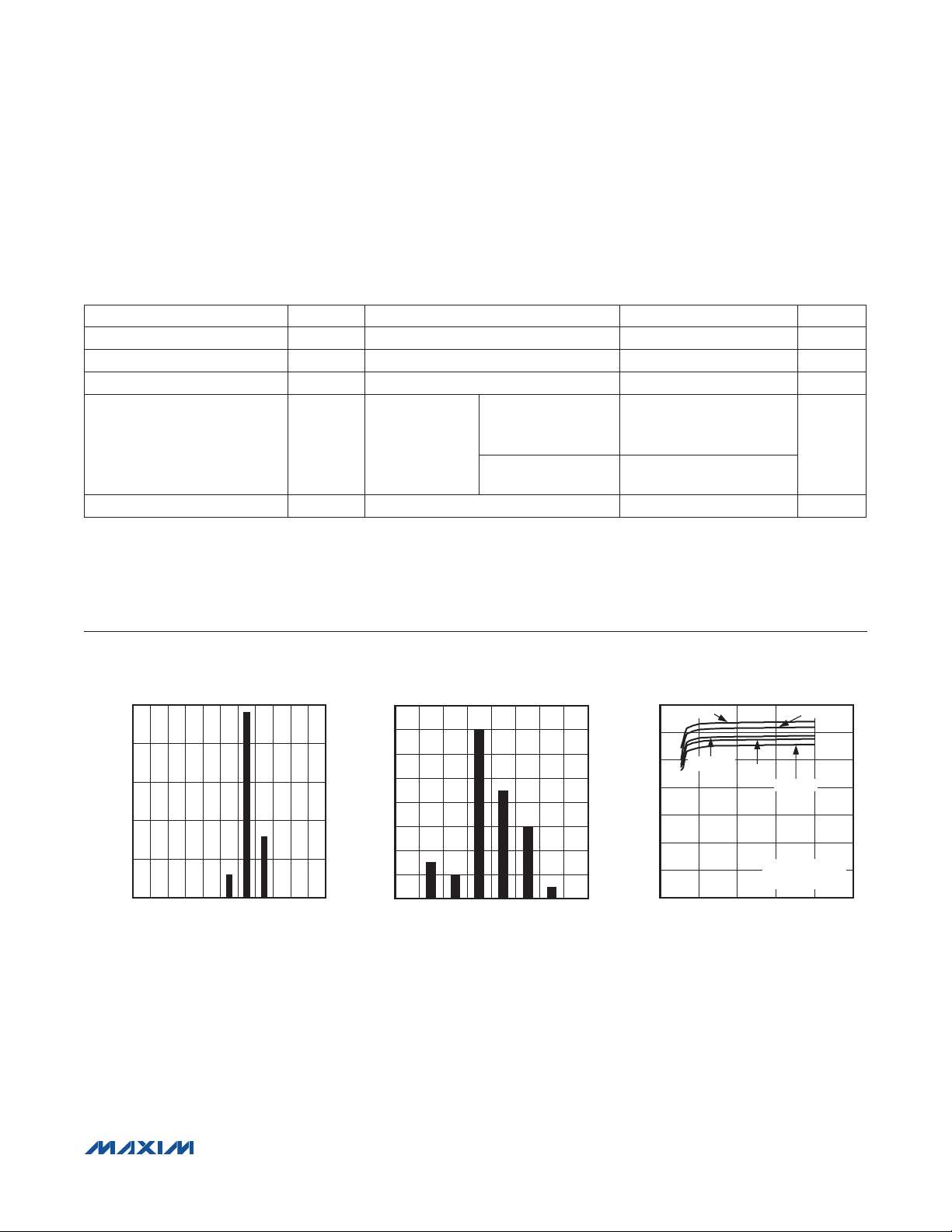
(VDD = 10V, VSS = 0V, outputs have RL = 10kI to VDD/2. TA = +25NC, unless otherwise specified.)
OFFSET VOLTAGE HISTOGRAM
25
20
15
10
FREQUENCY (%)
5
0
0 0.5 1.0 1.5 2.0 2.5 3.0 3.5 4.0 4.5 5.0
OFFSET VOLTAGE (µV)
MAX44251 toc01
INPUT OFFSET VOLTAGE DRIFT HISTOGRAM
16
14
12
10
8
6
FREQUENCY (%)
4
2
0
-0.00100.001
OFFSET VOLTAGE DRIFT (µV/°C)
0.002
0.003
0.004
0.005
MAX44251 toc02
0.006
SUPPLY CURRENT vs. SUPPLY VOLTAGE
1.4
TA = +125°C
1.2
1.0
0.8
0.6
SUPPLY CURRENT (mA)
0.4
0.2
TA = +25°C
0
SUPPLY VOLTAGE (V)
TA = 0°C
SUPPLY CURRENT
TA = +85°C
TA = -40°C
PER AMPLIFIER
2015105
MAX44251 toc03
5
����������������������������������������������������������������� Maxim Integrated Products 5
Page 6

MAX44251/MAX44252
TEMPERATURE (°C)
01
01
20V, Ultra-Precision, Low-Noise Op Amps
Typical Operating Characteristics (continued)
(VDD = 10V, VSS = 0V, outputs have RL = 10kI to VDD/2. TA = +25NC, unless otherwise specified.)
SUPPLY CURRENT vs. TEMPERATURE
1.28
1.26
1.24
1.22
1.20
1.18
1.16
1.14
SUPPLY CURRENT (mA)
1.12
1.10
1.08
1.06
-50 150
SUPPLY CURRENT
PER AMPLIFIER
INPUT BIAS CURRENT
vs. INPUT COMMON-MODE VOLTAGE
250
200
(pA)
BIAS
I
150
100
50
0
-50
-100
-150
-200
-250
NEGATIVE I
POSITIVE I
VCM (V)
BIAS
BIAS
INPUT OFFSET VOLTAGE
vs. INPUT COMMON MODE
6
(µV)
OS
V
5
4
3
2
1
0
8642
INPUT COMMON VOLTAGE (V)
MAX44251 toc04
12510050 750 25-25
MAX44251 toc05
0
(µV)
OS
V
6
5
4
3
2
1
0
INPUT BIAS CURRENT
vs. TEMPERATURE
1000
750
MAX44251 toc07
500
250
0
(pA)
BIAS
-250
I
-500
-750
-1000
8642
-1250
0
POSITIVE I
BIAS
NEGATIVE I
BIAS
TEMPERATURE (°C)
12510050 75025-25-50 150
MAX44251 toc08
160
140
120
100
80
60
CMRR (dB)
40
20
0
-20
INPUT OFFSET VOLTAGE
vs. TEMPERATURE
10050 75025-25-50 125
TEMPERATURE (°C)
COMMON-MODE REJECTION RATIO
vs. FREQUENCY
0.1 100M10M
FREQUENCY (Hz)
1M100k1k 10k10 1001
MAX44251 toc06
MAX44251 toc09
����������������������������������������������������������������� Maxim Integrated Products 6
Page 7

MAX44251/MAX44252
20V, Ultra-Precision, Low-Noise Op Amps
Typical Operating Characteristics (continued)
(VDD = 10V, VSS = 0V, outputs have RL = 10kI to VDD/2. TA = +25NC, unless otherwise specified.)
COMMON-MODE REJECTION RATIO
vs. TEMPERATURE
160
140
120
CMRR (dB)
100
80
60
TEMPERATURE (°C)
OUTPUT VOLTAGE SWING LOW
vs. TEMPERATURE
18
16
14
12
10
(mV)
OL
8
V
6
4
2
0
TEMPERATURE (°C)
10050 75025-25-50 125
RL = 10kI to VDD/2
12510050 75025-25-50 150
MAX44251 toc10
MAX44251 toc13
POWER-SUPPLY REJECTION RATIO
vs. FREQUENCY
160
140
120
100
80
60
PSRR (dB)
40
20
0
-20
-40
0.1 100M10M
FREQUENCY (Hz)
OPEN-LOOP GAIN vs. FREQUENCY
180
160
140
120
100
80
60
40
20
OPEN-LOOP GAIN (dB)
0
-20
-40
-60
FREQUENCY (Hz)
VCM = 0V
1M100k1k 10k10 1001
1M100k1k 10k10 10010.1 10M 100M
MAX44251 toc11
(mV)
OH
V
MAX44251 toc14
INPUT VOLTAGE NOISE (nV/√Hz)
OUTPUT VOLTAGE SWING HIGH
vs. TEMPERATURE
35
30
25
20
15
10
5
0
TEMPERATURE (°C)
RL = 10kI to VDD/2
INPUT VOLTAGE NOISE vs. FREQUENCY
30
25
20
15
10
5
0
10 100k
FREQUENCY (Hz)
10k1k100
MAX44251 toc12
12510050 75025-25-50 150
MAX44251 toc15
INPUT VOLTAGE 0.1Hz TO 10Hz NOISE
1s/div
MAX44251 toc16
����������������������������������������������������������������� Maxim Integrated Products 7
0.2µV/div
INPUT CURRENT NOISE vs. FREQUENCY
6
5
4
3
2
INPUT CURRENT NOISE (pA/√Hz)
1
0
1 10k
FREQUENCY (Hz)
2
SMALL-SIGNAL RESPONSE
0
MAX44251 toc17
-2
-4
-6
-8
-10
MAGNITUDE (dB)
-12
-14
VIN = 100mV
-16
1k10010
-18
1 100M
P-P
FREQUENCY (Hz)
MAX44251 toc18
10M1M10k 100k100 1k10
Page 8

MAX44251/MAX44252
20V, Ultra-Precision, Low-Noise Op Amps
Typical Operating Characteristics (continued)
(VDD = 10V, VSS = 0V, outputs have RL = 10kI to VDD/2. TA = +25NC, unless otherwise specified.)
5
0
-5
-10
-15
-20
-25
-30
MAGNITUDE (dB)
-35
-40
-45
-50
SUPPLY
VOLTAGE
(5V/div)
0V
0V
V
OFFSET
(10mV/div)
LARGE-SIGNAL RESPONSE
FREQUENCY (Hz)
POWER-UP TIME
VDD = VSS = 0V
VOLTAGE (1V/div)
TIME (10µs/div)
25µs
VIN = 2V
1M100k1k 10k10 10010.1 100M10M
VDD = 5V
VSS = 5V
P-P
MAX44251 toc22
MAX44251 toc19
MAGNITUDE (dB)
SMALL-SIGNAL STEP RESPONSE
vs. TIME
AV = 1V/V
= 100mV
V
IN
P-P
INPUT
OUTPUT
VOLTAGE (100mV/div)
TIME (2µs/div)
TOTAL HARMONIC DISTORTION
vs. FREQUENCY
-100
-105
-110
-115
-120
-125
-130
-135
-140
100 100k
FREQUENCY (Hz)
10k1k
MAX44251 toc20
MAX44251 toc23
LARGE-SIGNAL STEP RESPONSE
vs. TIME
AV = 1V/V
= 2V
V
IN
P-P
INPUT
VOLTAGE (1V/div)
OUTPUT
TIME (2µs/div)
TOTAL HARMONIC DISTORTION
vs. INPUT VOLTAGE
0
VCC = 3.3V
-20
-40
-60
-80
MAGNITUDE (dB)
-100
-120
-140
0.25 2.00
INPUT VOLTAGE (V)
MAX44251 toc21
MAX44251 toc24
1.751.501.251.000.750.50
STABILITY vs. CAPACITIVE AND
RESISTIVE LOAD IN PARALLEL WITH C
100
90
80
70
60
STABLE UNSTABLE
50
40
RESISTIVE LOAD (kI)
30
20
10
0
1k100 10k
CAPACITIVE LOAD (pF)
L
MAX44251 toc25
(I)
ISO
R
STABILITY vs. CAPACITIVE AND
IN SERIES WITH C
R
8
ISO
7
STABLE
6
5
4
3
2
1
0
100 100k
CAPACITIVE LOAD (pF)
LOAD
UNSTABLE
10k1k
MAX44251 toc26
����������������������������������������������������������������� Maxim Integrated Products 8
Page 9

TOP VIEW
51
OUTA
INA+
V
SS
1
2INA-
3
4
+
MAX44251
8 SOT23
MAX44251/MAX44252
20V, Ultra-Precision, Low-Noise Op Amps
Pin Configurations
+
87V
6
5
DD
OUTB
INB-
INB+
OUTA
INA-
INA+
1
OUTA
2
+
1
2
MAX44251
3
4
SS
8
V
DD
7
OUTB
6
INB-
5
INB+V
8 µMAX
INA+
V
DD
INB- 6
MAX44252
3
4
7
14 SOIC
1413OUTD
IND-INA-
IND+
12
V
11
SS
0 INC+INB+
9
INC-
8
OUTCOUTB
PIN
SOT23 µMAX SOIC
NAME FUNCTION
1 1 1 OUTA Channel A Output
2 2 2 INA- Channel A Negative Input
3 3 3 INA+ Channel A Positive Input
4 4 11 V
SS
Negative Supply Voltage
5 5 5 INB+ Channel B Positive Input
6 6 6 INB- Channel B Negative Input
7 7 7 OUTB Channel B Output
8 8 4 V
DD
Positive Supply Voltage
— — 8 OUTC Channel C Output
— — 9 INC- Channel C Negative Input
— — 10 INC+ Channel C Positive Input
— — 12 IND+ Channel D Positive Input
— — 13 IND- Channel D Negative Input
— — 14 OUTD Channel B Output
Pin Description
����������������������������������������������������������������� Maxim Integrated Products 9
Page 10

MAX44251/MAX44252
20V, Ultra-Precision, Low-Noise Op Amps
Detailed Description
The MAX44251/MAX44252 are high-precision amplifiers
that have less than 3FV of typical input-referred offset
and low flicker noise. These characteristics are achieved
through an autozeroing technique that samples and finds
repeating patterns of signal to cancel the input offset voltage and 1/f noise of the amplifier.
Autozero
The ICs feature an autozero circuit that allows the devices
to achieve less than 6FV (max) of input offset voltage at
room temperature and eliminate the 1/f noise.
Noise Suppression
Flicker noise, inherent in all active devices, is inversely
proportional to frequency presented. Charges at the
oxide-silicon interface that are trapped-and-released by
MOSFET oxide occurs at low frequency more often. For
this reason, flicker noise is also called 1/f noise.
Electromagnetic interference (EMI) noise occurs at higher frequency that results in malfunction or degradation of
electrical equipment.
The ICs have an input EMI filter to avoid the output getting affected by radio frequency interference. The EMI
filter composed of passive devices presents significant
higher impedance to higher frequency.
High Supply Voltage Range
The ICs feature 1.15mA current consumption per channel
and a voltage supply range from either 2.7V to 20V single
supply or ±1.35V to ±10V split supply.
Applications Information
The ICs are ultra-high-precision operational amplifiers with
a high supply voltage range designed for load cell, medical instrumentation and precision instrument applications.
These devices are also designed to interface with pressure transducers and are ideal for precision weight scale
application as shown in Figure 1.
ADC Buffer Amplifier
The MAX44251/MAX44252's low input offset voltage, low
noise, and fast settling time make these amplifiers ideal
for ADC buffers. Weigh scales are one application that
often require a low-noise, high-voltage amplifier in front
of an ADC. Figure 1 details an example of a load cell and
amplifier driven from the same Q10V supplies, along with
the MAX11211 18-bit delta sigma ADC. Load cells produce a very small voltage change at their outputs, therefore driving the excitation source with a higher voltage
produces a wider dynamic range that can be measured
at the ADC inputs.
The MAX11211 ADC operates from a single 2.7V to 3.6V
analog supply, offers 18-bit noise-free resolution and
0.86mW power dissipation. The MAX11211 also offers
> 100dB rejection at 50Hz and 60Hz. This ADC is part of
a family of 16-, 18-, 20-, and 24-bit delta sigma ADCs with
high precision and < 1mW power dissipation.
The MAX44251/MAX44252's low input offset voltage and
low noise allow a gain circuit prior to the MAX11211 without losing any dynamic range at the ADC.
20V
R
G
BUFFER
50R
50R
20V
BUFFER
G
G
20V
Figure 1. Weight Scale Application Circuit
���������������������������������������������������������������� Maxim Integrated Products 10
MAX44251
MAX44251
3.3V
3V
V
R
R
1.5V
20V
BUFFER
MAX44251
V
IN+
V
IN-
V
DD
MAX11211
V
V
REF
OUTPUT
SS
C
R
R
OUT
R
1
MAX6126
1
V
DD
MICRO
PROCESSOR
Page 11

MAX44251/MAX44252
20V, Ultra-Precision, Low-Noise Op Amps
Error Budget Example
When using the ICs as an ADC buffer in strain gauge
application, the temperature drift should be taken into
consideration to determine maximum input signal. A
typical strain gauge has sensitivity specification of just
2mV/V at rated out load. This means that when the strain
gauge load cell is powered with 10V, the full-scale output
voltage is 20mV. In this application, both offset voltage
and drift are critical parameters that directly affect the
accuracy of measurement. Even though offset voltage
could be calibrated out, its drift over temperature is still
a problem.
The ICs, with a typical offset drift of 5nV/°C, guarantee
that the drift over a 10°C range is only 50nV. Setting this
equal to 0.5 LSB in a 18-bit system yields a full-scale
range of 13mV. With a single 10V supply, an acceptable
closed-loop gain of 770V/V provides sufficient gain while
maintaining headroom.
Precision Low-Side Current Sensing
The ICs’ autozero feature produces ultra-low offset
voltage and drift, making them ideal for precision current-sensing applications. Figure 2 shows the ICs in
a low-side current-sense configuration. This circuit produces an accurate output voltage, V
x R
SENSE
x R2/R1.
equal to I
OUT
LOAD
Chip Information
PROCESS: BiCMOS
Ordering Information
PART TEMP RANGE
MAX44251AKA+
MAX44251AUA+
MAX44252ASD+*
-40NC to +125NC
-40NC to +125NC 8 FMAX
-40NC to +125NC
+Denotes a lead(Pb)-free/RoHS-compliant package.
*Future product—contact factory for availability.
Functional Diagrams
TOP VIEW
OUTA
INA+
+
1
2
3
4
SS
MAX44251
PINPACKAGE
TOP
MARK
8 SOT23 AERC
—
14 SOIC —
87V
DD
OUTBINA-
INB-
6
INB+V
5
V
SUPPLY
I
LOAD
R
1
R
SENSE
Figure 2. Low-Side Current Sensing
���������������������������������������������������������������� Maxim Integrated Products 11
R
2
MAX44251
MAX44252
OUT
OUTA
INA+
V
INB+
INB-
OUTB
+
1
2
3
4
DD
5
6
7
MAX44252
1413OUTD
IND-INA-
IND+
12
V
11
SS
10
INC+
9
INC-
8
OUTC
Page 12

MAX44251/MAX44252
20V, Ultra-Precision, Low-Noise Op Amps
Package Information
For the latest package outline information and land patterns (footprints), go to www.maxim-ic.com/packages. Note that a “+”, “#”, or
“-” in the package code indicates RoHS status only. Package drawings may show a different suffix character, but the drawing pertains
to the package regardless of RoHS status.
PACKAGE TYPE PACKAGE CODE OUTLINE NO. LAND PATTERN
8 SOT23 K8+5
8 FMAX
14 SOIC S14M+5
U8+1
21-0078 90-0176
21-0036 90-0092
21-0041 90-0096
���������������������������������������������������������������� Maxim Integrated Products 12
Page 13

MAX44251/MAX44252
20V, Ultra-Precision, Low-Noise Op Amps
Package Information (continued)
For the latest package outline information and land patterns (footprints), go to www.maxim-ic.com/packages. Note that a “+”, “#”, or
“-” in the package code indicates RoHS status only. Package drawings may show a different suffix character, but the drawing pertains
to the package regardless of RoHS status.
α
α
���������������������������������������������������������������� Maxim Integrated Products 13
Page 14

MAX44251/MAX44252
20V, Ultra-Precision, Low-Noise Op Amps
Package Information (continued)
For the latest package outline information and land patterns (footprints), go to www.maxim-ic.com/packages. Note that a “+”, “#”, or
“-” in the package code indicates RoHS status only. Package drawings may show a different suffix character, but the drawing pertains
to the package regardless of RoHS status.
���������������������������������������������������������������� Maxim Integrated Products 14
Page 15

MAX44251/MAX44252
20V, Ultra-Precision, Low-Noise Op Amps
Revision History
REVISION
NUMBER
0 10/11 Initial release —
REVISION
DATE
DESCRIPTION
PAGES
CHANGED
Maxim cannot assume responsibility for use of any circuitry other than circuitry entirely embodied in a Maxim product. No circuit patent licenses are implied.
Maxim reserves the right to change the circuitry and specifications without notice at any time.
Maxim Integrated Products, 120 San Gabriel Drive, Sunnyvale, CA 94086 408-737-7600 15
©
2011 Maxim Integrated Products Maxim is a registered trademark of Maxim Integrated Products, Inc.
 Loading...