

Page 1

General Description
The MAX4399 audio/video switch is ideal for digital settop box applications. The MAX4399 provides video and
audio routing from the MPEG decoder source to the TV,
VCR, and AUX SCART (peritelevision) connectors. In
addition, the TV audio channel features clickless
switching and programmable volume control from
-56dB to +6dB in 2dB steps. The device can mix an
auxiliary audio tone into the TV audio channel and can
mix the stereo audio signal into a mono audio signal.
The MAX4399 directly drives an external RF modulator
with a composite video with blanking and sound
(CVBS) signal created by an on-chip luma/chroma
(Y/C) mixer and external RLC trap filter. The MAX4399
features a fast-mode I2C™-compatible 2-wire interface
allowing communication at data rates up to 400kbps.
The MAX4399 operates with standard +5V and +12V
single supplies and supports slow and fast switching.
All video and audio inputs are AC-coupled. The DC
biases of all input and output signals are set to predefined levels. All video outputs, including the RF modulator, drive standard 150Ω loads. Red, green, and
blue (RGB) outputs feature a programmable gain of
+6dB ±1dB. All other video outputs have a fixed +6dB
gain. The VCR and AUX audio output gains are programmable for -6dB, 0dB, and +6dB.
The MAX4399 is available in a compact 68-pin thin
QFN package and is specified for the 0°C to +70°C
commercial temperature range. The MAX4399 evaluation kit is available to help speed designs.
Applications
Satellite Receivers
Satellite Set-Top Boxes
Cable Set-Top Boxes
Terrestrial Set-Top Boxes
Game Consoles
TVs
Digital Television (DTV)
VCRs
DVD Players
DVD+R/W Players
Features
♦ Low -86dB Video Signal-to-Noise Ratio
♦ 150Ω Driver on All Video Outputs, Including the
RF Modulator
♦ Full CVBS Loop-Through on AUX SCART
♦ Programmable Audio Gain Control of -56dB to
+6dB (TV Audio Outputs)
♦ Clickless Audio Switching (TV Audio Outputs)
♦ Programmable Clamp or Bias on Red/Chroma
Video Inputs
♦ Programmable Video Gain of +6dB, ±1dB on RGB
Outputs
♦ +5V and +12V Standard Supply Voltages
♦ 27MHz -3dB Large-Signal Bandwidth on All Video
Drivers
♦ Supports Three SCART Connectors
MAX4399
Audio/Video Switch for Three SCART
Connectors
________________________________________________________________ Maxim Integrated Products 1
Ordering Information
MAX4399
SCART
SWITCH
MATRIX
I
2
C-COMPATIBLE
2-WIRE INTERFACE
STB
ENCODER
RGB
S-VHS
CVBS
R/L AUDIO
FAST SWITCHING
VCR SCART
CONNECTOR
TONE INPUT
CVBS
S-VHS
RGB
R/L AUDIO
FAST SWITCHING
SLOW SWITCHING
TV SCART
CONNECTOR
AUXILIARY
SCART
CONNECTOR
CHANNEL
3/4 RF
MODULATOR
SUBCARRIER TRAP
CVBS
S-VHS
RGB
R/L AUDIO
SLOW SWITCHING
FAST SWITCHING
CVBS
MONO AUDIO
R/L PHONO AUDIO
CVBS
S-VHS
R/L AUDIO
SLOW SWITCHING
VIDEO
GROUND
DIGITAL
GROUND
AUDIO
GROUND
VIDEO
+5V
DIGITAL
+5V
AUDIO
+12V
SATELLITE DISH
Typical Operating Circuit
19-2925; Rev 0; 8/03
For pricing, delivery, and ordering information, please contact Maxim/Dallas Direct! at
1-888-629-4642, or visit Maxim’s website at www.maxim-ic.com.
EVALUATION KIT
AVAILABLE
Purchase of I2C components of Maxim Integrated Products,
Inc. or one of its sublicensed Associated Companies, conveys
a license under the Philips I
2
C Patent Rights to use these com-
ponents in an I
2
C system, provided that the system conforms
to the I
2
C Standard Specification as defined by Philips.
PART TEMP RANGE PIN-PACKAGE
MAX4399CTK 0°C to +70°C 68 Thin QFN
Page 2

MAX4399
Audio/Video Switch for Three SCART
Connectors
2 _______________________________________________________________________________________
ABSOLUTE MAXIMUM RATINGS
Stresses beyond those listed under “Absolute Maximum Ratings” may cause permanent damage to the device. These are stress ratings only, and functional
operation of the device at these or any other conditions beyond those indicated in the operational sections of the specifications is not implied. Exposure to
absolute maximum rating conditions for extended periods may affect device reliability.
Voltages
V_VID to G_VID .....................................................-0.3V to +6V
V12 to G_AUD .....................................................-0.3V to +14V
V_DIG to G_DIG ....................................................-0.3V to +6V
G_AUD to G_DIG ...............................................-0.1V to +0.1V
G_VID to G_DIG .................................................-0.1V to +0.1V
G_AUD to G_VID ................................................-0.1V to +0.1V
Video Inputs, Video Outputs, ENC_FS_IN, VCR_FS_IN,
VID_BIAS, TRAP ................................-0.3V to (V
V_VID
+ 0.3V)
V_AUD to G_AUD................................................-0.3V to +9V
Audio Inputs, Audio Outputs,
AUD_BIAS........................................-0.3V to (V
V_AUD
+ 0.3V)
SDA, SCL, DEV_ADDR, INTERRUPT_OUT .........-0.3V to +6V
AUX_SS, TV_SS, VCR_SS ....................-0.3V to (V
V12
+ 0.3V)
Currents
INTERRUPT_OUT ..........................................................+50mA
TRAP................................................................................±4mA
Output Short Circuit
Video Outputs and TV_FS_OUT to V_VID,
V_DIG, G_AUD, G_VID, or G_DIG ........................Continuous
Audio Outputs to V_AUD, V_VID, V_DIG,
G_AUD, G_VID, or G_DIG.....................................Continuous
AUX_SS, TV_SS, and VCR_SS to V12,
V_AUD, V_VID, V_DIG, G_AUD,
G_VID, or G_DIG...................................................Continuous
Continuous Power Dissipation (T
A
= +70°C)
68-Pin Thin QFN (derate 41.7mW/°C
above +70°C).........................................................3333.3mW
Operating Temperature Range...............................0°C to +70°C
Junction Temperature......................................................+150°C
Storage Temperature Range .............................-65°C to +150°C
Lead Temperature (soldering, 10s) .................................+300°C
ELECTRICAL CHARACTERISTICS
(V
V12
= 12V, V
V_VID
= 5V, V
V_DIG
= 5V, 0.47µF X5R capacitor in parallel with a 10µF aluminum electrolytic capacitor from V_AUD to
G_AUD, no load, T
A
= 0°C to +70°C, unless otherwise noted. Typical values are at TA= +25°C.) (Note 1)
DC
V12 Supply Voltage Range Inferred from the slow switch output levels 11.4 12 12.6 V
V_VID Supply Voltage Range
V_DIG Supply Voltage Range 4.75 5 5.25 V
V12 Quiescent Supply Current 17 35 mA
V_VID Quiescent Supply Current
V_VID Standby Supply Current
V_DIG Quiescent Supply Current 13mA
VIDEO
Voltage Gain 1V
Small-Signal Bandwidth, -3dB
Large-Signal Bandwidth, -3dB
PARAMETER SYMBOL CONDITIONS MIN TYP MAX UNITS
Inferred from the output swing of the video
outputs
All video output amplifiers are enabled, no
load
All video output amplifiers are in shutdown,
and TV_FS_OUT driver is in shutdown
input
P-P
100mV
gain = 6dB
1V
= 6dB, T
+25°C (Note 2)
P-P
input, gain
P-P
=
A
input,
CVBS and S-VHS 5.5 6 6.5
R, G, B, gain = 5dB 4.5 5 5.5
R, G, B, gain = 6dB 5.5 6 6.5
R, G, B, gain = 7dB 6.5 7 7.5
CVBS and S-VHS 110
R, G, B 110
CVBS and S-VHS 15 27
R, G, B 30
4.75 5 5.25 V
51 116 mA
19 34 mA
MHz
MHz
dB
Page 3
MAX4399
Audio/Video Switch for Three SCART
Connectors
_______________________________________________________________________________________ 3
ELECTRICAL CHARACTERISTICS (continued)
(V
V12
= 12V, V
V_VID
= 5V, V
V_DIG
= 5V, 0.47µF X5R capacitor in parallel with a 10µF aluminum electrolytic capacitor from V_AUD to
G_AUD, no load, T
A
= 0°C to +70°C, unless otherwise noted. Typical values are at TA= +25°C.) (Note 1)
Slew Rate SR 1V
Gain Matching 1V
Differential Gain DG
Differential Phase DP
Signal-to-Noise Ratio SNR 1V
Group Delay
Bottom Level Clamp
Chroma Bias Chroma only, no signal, no load 1.88 V
Sync Crush
Power-Supply Rejection Ratio PSRR f = 100kHz, 0.5V
Input Impedance
Input Clamp Current VIN = 1.75V 2.5 4.2 8.0 µA
Output Bias Voltage
Pulldown Resistance
Crosstalk
Mute Suppression f = 4.43MHz, 1V
AUDIO
V_AUD Voltage Generated by internal linear regulator 8.1 V
Voltage Gain 1.414V
Gain Matching Between
Channels
Gain Flatness
Frequency Bandwidth
PARAMETER SYMBOL CONDITIONS MIN TYP MAX UNITS
input, gain = 6dB 170 V/µs
P-P
input, between RGB or Y-C -0.5 0 +0.5 dB
P-P
5-step
modulated
staircase
5-step
modulated
staircase
input -86 dB
P-P
f = 0.1MHz to
6MHz
RGB, composite and luma, no signal, no
load
Percentage reduction in sync pulse
(0.3V
current with a 0.1µF coupling capacitor
CVBS, Y, or RGB video input 4 MΩ
Chroma video input 11 kΩ
No signal, no
load
VCR_R/C_OUT, AUX_R/C_OUT,
TV_R/C_OUT
f = 4.43MHz, 1V
active inputs
1.414V
f = 20Hz to 20kHz, 0.5V
0dB
0.5V
-3dB with 1kHz serving as 0dB
); inferred from input clamping
P-P
P-P
P-P
input; frequency where output is
RMS
RF_CVBS_OUT 0.03
All other video outputs 0.13
RF_CVBS_OUT 0.09
All other video outputs 0.36
RF_CVBS_OUT 5
All other video outputs 3
P-P
RGB, composite, and
luma
Chroma 2.24
input, between any two
P-P
input, on one input -65 dB
P-P
input, gain = 0dB -0.25 0 +0.25 dB
input, gain = 0dB -0.5 0 +0.5 dB
input, gain =
RMS
degrees
1.21 V
-2 0 +2 %
60 dB
1.05
10 Ω
-63 dB
0.005 dB
210 kHz
%
ns
V
Page 4
MAX4399
Audio/Video Switch for Three SCART
Connectors
4 _______________________________________________________________________________________
ELECTRICAL CHARACTERISTICS (continued)
(V
V12
= 12V, V
V_VID
= 5V, V
V_DIG
= 5V, 0.47µF X5R capacitor in parallel with a 10µF aluminum electrolytic capacitor from V_AUD to
G_AUD, no load, T
A
= 0°C to +70°C, unless otherwise noted. Typical values are at TA= +25°C.) (Note 1)
Input DC Level Gain = 0dB V_AUD/2 V
Input Signal Amplitude
Input Resistance 100 kΩ
Output DC Level V_AUD/2 V
Signal-to-Noise Ratio SNR
Total Harmonic Distortion THD R
Output Impedance 0.5 Ω
Volume Attenuation Step
Power-Supply Rejection Ratio PSRR f = 1kHz, 0.5V
Mute Suppression f = 1kHz, 0.5V
Audio Limiter Level f = 1kHz, 2.5V
Crosstalk f = 1kHz, 0.5V
DIGITAL INTERFACE: SDA and SCL
Low-Level Input Voltage V
High-Level Input Voltage V
Hysteresis of Schmitt Trigger
Input
SDA Low-Level Output Voltage V
Output Fall Time for SDA Line 400pF bus load 250 ns
Spike Suppression 50 ns
Input Current VIL = 0V, VIH = 5V -10 +10 µA
Input Capacitance 5pF
SCL Clock Frequency 0 400 kHz
Hold Time t
Low Period of SCL Clock t
High Period of SCL Clock t
Setup Time for a Repeated Start
Condition
Data Hold Time t
Data Setup Time t
Maximum Receive SCL/SDA Rise
Time
PARAMETER SYMBOL CONDITIONS MIN TYP MAX UNITS
Inferred through total harmonic distortion
specification, f = 1kHz
IL
IH
OL
HD,STA
LOW
HIGH
t
SU,STA
HD,DAT
SU,DAT
t
R
f = 1.0kHz, 1V
20kHz
= 10kΩ
LOAD
1.414V
P-P
input
I
= 3mA 0 0.4
SINK
I
= 6mA 0 0.6
SINK
Repeated start condition 0.6 µs
(Note 3) 300 ns
, gain = 0dB, 20Hz to
RMS
f = 1.0kHz, 0.5V
f = 1.0kHz, 2V
TV audio, volume control
range extends from -56dB
to +6dB
VCR, AUX audio 5.5 6 6.5
P-P
input 105 dB
RMS
input 6.7 V
RMS
, gain = 0dB 105 dB
RMS
RMS
RMS
2V
105 dB
0.002
0.005
1.5 2 2.5
110 dB
0.8 V
2.6 V
0.2 V
1.3 µs
0.6 µs
0.6 µs
0 0.9 µs
100 ns
RMS
dB
%
P-P
V
Page 5
MAX4399
Audio/Video Switch for Three SCART
Connectors
_______________________________________________________________________________________ 5
ELECTRICAL CHARACTERISTICS (continued)
(V
V12
= 12V, V
V_VID
= 5V, V
V_DIG
= 5V, 0.47µF X5R capacitor in parallel with a 10µF aluminum electrolytic capacitor from V_AUD to
G_AUD, no load, T
A
= 0°C to +70°C, unless otherwise noted. Typical values are at TA= +25°C.) (Note 1)
Note 1: All devices are 100% tested at TA= +25°C. All temperature limits are guaranteed by design.
Note 2: Parameter guaranteed by design.
Note 3: C
B
= total capacitance of one bus line in pF. Tested with CB= 400pF.
Minimum Receive SCL/SDA Rise
Time (Note 3)
Maximum Receive SCL/SDA Fall
Time (Note 3)
Minimum Receive SCL/SDA Fall
Time (Note 3)
Setup Time for Stop Condition t
Bus Free Time Between a Stop
and Start
OTHER DIGITAL PINS
DEV_ADDR Low Level 0.8 V
DEV_ADDR High Level 2.6 V
INTERRUPT_OUT Low Voltage INTERRUPT_OUT sinking 1mA 0.15 0.4 V
INTERRUPT_OUT High Leakage
Current
SLOW SWITCHING
Input Low Level 02V
Input Medium Level 4.5 7.0 V
Input High Level 9.5 12.0 V
Input Current 50 100 µA
Output Low Level R
Output Medium Level (External
16/9)
Output High Level (External 4/3) R
FAST SWITCHING
Input Low Level 0 0.4 V
Input High Level 13V
Input Current 110µA
Output Low Level I
Output High Level V_VID - VOH, I
Fast-Switching Output to RGB
Skew
Fast-Switching Output Rise Time R
Fast-Switching Output Fall Time R
PARAMETER SYMBOL CONDITIONS MIN TYP MAX UNITS
t
R
t
F
t
F
SU,STO
t
BUF
V
INTERRUPT_OUT
= 10kΩ to ground 0 1.5 V
LOAD
R
= 10kΩ to ground 5.0 6.5 V
LOAD
= 10kΩ to ground 10 12 V
LOAD
= 0.5mA 0 0.01 0.2 V
SINK
Difference in propagation delays of fastswitching signal and RGB signals;
measured from 50% input transition to 50%
output transition
= 150Ω to ground 30 ns
LOAD
= 150Ω to ground 30 ns
LOAD
= 5V 1 10 µA
= 20mA 0.75 2 V
SOURCE
20 +
0.1C
B
300 ns
20 +
0.1C
B
0.6 µs
1.3 µs
30 ns
ns
ns
Page 6

MAX4399
Audio/Video Switch for Three SCART
Connectors
6 _______________________________________________________________________________________
Typical Operating Characteristics
(V
V12
= 12V, V
V_VID
= 5V, V
V_DIG
= 5V, 0.47µF ceramic X5R capacitor in parallel with a 10µF aluminum electrolytic capacitor from
V_AUD to G_AUD, no load, T
A
= +25°C, unless otherwise noted.)
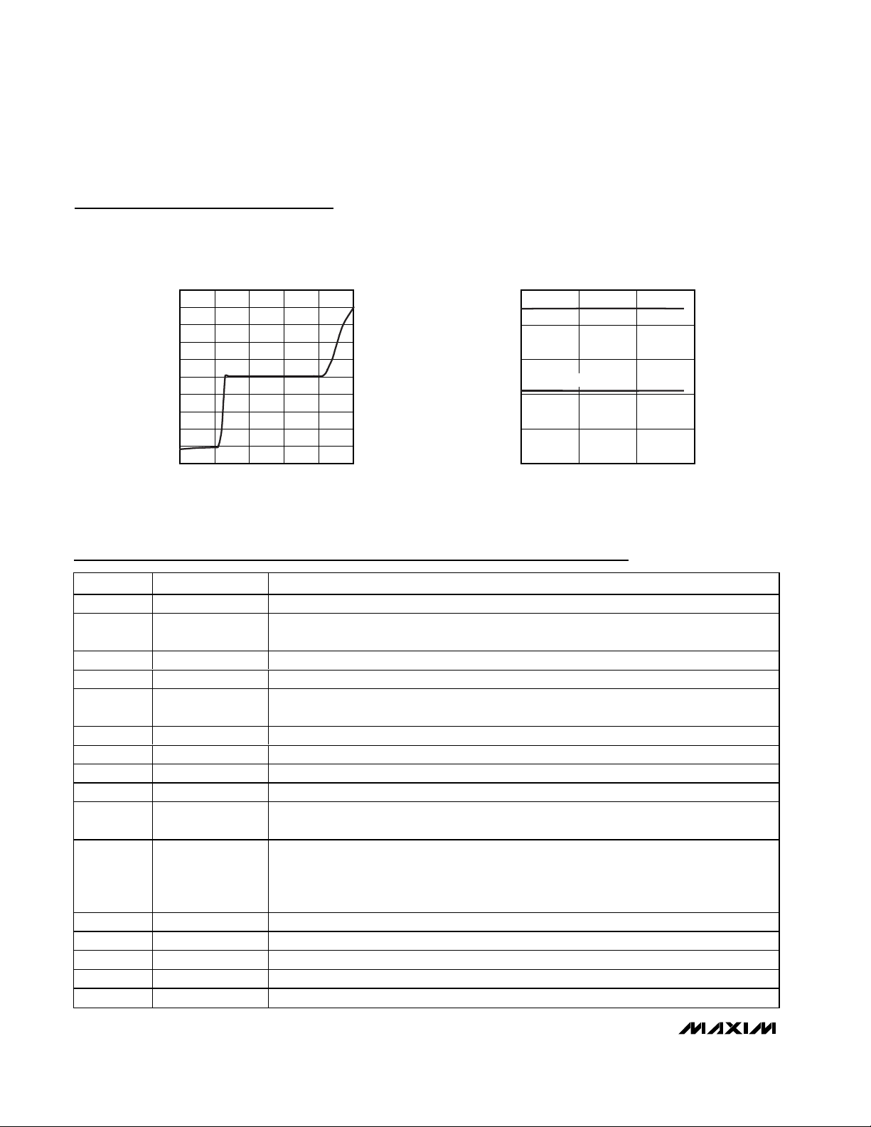
RGB VIDEO LARGE-SIGNAL BANDWIDTH
vs. FREQUENCY
MAX4399 toc01
FREQUENCY (MHz)
GAIN (dB)
101
-5
-4
-3
-2
-1
0
1
2
3
4
-6
0.1 100
VIN = 1V
P-P
RL = 150Ω to G_VID
Y VIDEO LARGE-SIGNAL BANDWIDTH
vs. FREQUENCY
MAX4399 toc02
FREQUENCY (MHz)
GAIN (dB)
101
-5
-4
-3
-2
-1
0
1
2
3
4
-6
0.1 100
VIN = 1V
P-P
RL = 150Ω to G_VID
RGB VIDEO SMALL-SIGNAL BANDWIDTH
vs. FREQUENCY
MAX4399 toc03
FREQUENCY (MHz)
GAIN (dB)
101
-5
-4
-3
-2
-1
0
1
2
3
4
-6
0.1 100
1000
V
IN
= 100mV
P-P
RL = 150Ω to G_VID
Y VIDEO SMALL-SIGNAL BANDWIDTH
vs. FREQUENCY
MAX4399 toc04
FREQUENCY (MHz)
GAIN (dB)
101
-5
-4
-3
-2
-1
0
1
2
3
4
-6
0.1 100
VIN = 100mV
P-P
RL = 150Ω to G_VID
VIDEO CROSSTALK
vs. FREQUENCY
MAX4399 toc05
FREQUENCY (MHz)
CROSSTALK (dB)
101
-90
-80
-70
-60
-50
-40
-30
-20
-10
0
-100
0.1 100
VIN = 100mV
P-P
RL = 150Ω to G_VID
RF_CVBS_OUT (WITH TRAP FILTER)
MAX4399 toc06
DIFFERENTIAL PHASE (deg)
1324567
1324567
DIFFERENTIAL GAIN (%)
0.2
0.1
0
-0.2
-0.1
0.2
0.1
0
-0.2
-0.1
R
L
= 150Ω to G_VID
R
L
= 150Ω to G_VID
RF_CVBS_OUT (WITHOUT TRAP FILTER)
MAX4399 toc07
DIFFERENTIAL PHASE (deg)
DIFFERENTIAL GAIN (%)
RL = 150Ω to G_VID
R
L
= 150Ω to G_VID
0.2
0.1
0
-0.2
-0.1
0.2
0.1
0
-0.2
-0.1
1324567
1324567
TV_Y/CVBS_OUT
MAX4399 toc08
DIFFERENTIAL PHASE (deg)
1324567
1324567
DIFFERENTIAL GAIN (%)
RL = 150Ω to G_VID
R
L
= 150Ω to G_VID
0.5
0.3
0.1
-0.3
-0.1
0.2
0.1
0
-0.2
-0.1
-0.5
AUDIO LARGE-SIGNAL
BANDWIDTH vs. FREQUENCY
MAX4399 toc09
FREQUENCY (kHz)
GAIN (dB)
100101
-15
-12
-9
-6
-3
0
3
-18
0.1 1000
VIN = 0.5V
RMS
RL = 10kΩ to G_AUD
Page 7

MAX4399
Audio/Video Switch for Three SCART
Connectors
_______________________________________________________________________________________ 7
Typical Operating Characteristics (continued)
(V
V12
= 12V, V
V_VID
= 5V, V
V_DIG
= 5V, 0.47µF ceramic X5R capacitor in parallel with a 10µF aluminum electrolytic capacitor from
V_AUD to G_AUD, no load, T
A
= +25°C, unless otherwise noted.)
AUDIO CROSSTALK vs. FREQUENCY
0
RL = 10kΩ to G_AUD
-10
-20
-30
-40
-50
-60
-70
CROSSTALK (dB)
-80
V = 0.5V
-90
-100
-110
-120
0.01 100
RMS
1010.1
FREQUENCY (kHz)
V_VID STANDBY QUIESCENT SUPPLY
CURRENT vs. TEMPERATURE
30
ALL VIDEO OUTPUT
AMPLIFIERS DISABLED
25
20
15
10
5
V_VID STANDBY SUPPLY CURRENT (mA)
0
0 255075
TEMPERATURE (°C)
V_VID QUIESCENT SUPPLY
CURRENT vs. TEMPERATURE
60
ALL VIDEO OUTPUT
58
AMPLIFIERS ENABLED
56
54
52
50
48
46
44
42
40
0 255075
TEMPERATURE (°C)
V12 QUIESCENT SUPPLY CURRENT
vs. TEMPERATURE
30
25
20
15
10
5
0
0 255075
TEMPERATURE (°C)
1
MAX4399 toc10
0.1
0.01
THD+N (%)
0.001
0.0001
0.01 100
2.0
MAX4399 toc13
1.8
1.6
1.4
1.2
1.0
0.8
0.6
V_DIG SUPPLY CURRENT (mA)
0.4
0.2
0
025
AUDIO THD+N vs. FREQUENCY
RL = 10kΩ to G_AUD
V = 1.5V
RMS
V = 1.0V
RMS
V = 0.5V
RMS
1010.1
FREQUENCY (kHz)
V_DIG QUIESCENT SUPPLY CURRENT
vs. TEMPERATURE
50
TEMPERATURE (°C)
MAX4399 toc11
V_VID QUIESCENT SUPPLY CURRENT (mA)
MAX4399 toc14
V12 SUPPLY CURRENT (mA)
75
MAX4399 toc12
MAX4399 toc15
V_AUD vs. TEMPERATURE
INPUT CLAMP AND BIAS LEVEL
10.0
9.5
9.0
8.5
8.0
V_AUD (V)
7.5
7.0
6.5
6.0
075
TEMPERATURE (°C)
5025
2.5
2.3
MAX4399 toc16
2.1
BIAS
1.9
1.7
1.5
BOTTOM-LEVEL
CLAMP
1.3
1.1
0.9
INPUT CLAMP AND BIAS LEVEL (V)
0.7
0.5
075
vs. TEMPERATURE
5025
TEMPERATURE (°C)
MAX4399 toc17
INPUT CLAMP CURRENT
vs. TEMPERATURE
6.0
VIN = 1.75V
5.5
5.0
4.5
4.0
3.5
3.0
2.5
INPUT CLAMP CURRENT (µA)
2.0
1.5
1.0
025
TEMPERATURE (°C)
MAX4399 toc18
50
75
Page 8
MAX4399
Audio/Video Switch for Three SCART
Connectors
8 _______________________________________________________________________________________
Pin Description
Typical Operating Characteristics (continued)
(V
V12
= 12V, V
V_VID
= 5V, V
V_DIG
= 5V, 0.47µF ceramic X5R capacitor in parallel with a 10µF aluminum electrolytic capacitor from
V_AUD to G_AUD, no load, T
A
= +25°C, unless otherwise noted.)
INPUT CLAMP CURRENT
vs. INPUT VOLTAGE
MAX4399 toc19
INPUT VOLTAGE (V)
INPUT CLAMP CURRENT (mA)
4321
-0.4
-0.3
-0.2
-0.1
0
0.1
0.2
0.3
0.4
0.5
-0.5
05
OUTPUT BIAS VOLTAGE
vs. TEMPERATURE
MAX4399 toc20
TEMPERATURE (°C)
OUTPUT BIAS VOLTAGE (V)
5025
0.5
1.0
1.5
2.0
2.5
0
075
RGB, LUMA, CVBS
CHROMA
PIN NAME FUNCTION
1 V_DIG Digital Supply Voltage. Connect to 5V.
2 DEV_ADDR
Device Address Set Input. Connect to G_DIG to set write and read addresses of 94h and 95h,
respectively. Connect to V_DIG to set write and read addresses of 96h and 97h, respectively.
3 SDA Bidirectional Data I/O. I2C-compatible, 2-wire interface data input/output. Output is open drain.
4 SCL Clock Input. I2C-compatible, 2-wire interface clock.
5 INTERRUPT_OUT
Interrupt Output. INTERRUPT_OUT is an open-drain output that goes high impedance to
indicate a change in the slow switch lines, AUX_SS, TV_SS, or VCR_SS.
6 G_DIG Digital Ground
7 ENC_L_IN Digital Encoder Left-Channel Audio Input
8 ST_AUX_IN Satellite Dish Tone Input
9 ENC_R_IN Digital Encoder Right-Channel Audio Input
10 AUD_BIAS
Audio Input Bias Voltage. Bypass AUD_BIAS with a 10µF capacitor and a 0.1µF capacitor to
G_AUD.
Audio Supply Voltage. Connect all V_AUD together. An on-board linear regulator creates the
11, 22, 30 V_AUD
12 AUX_L_IN AUX SCART Left-Channel Audio Input
13 AUX_R_IN AUX SCART Right-Channel Audio Input
14 VCR_R_IN VCR SCART Right-Channel Audio Input
15 VCR_L_IN VCR SCART Left-Channel Audio Input
16 TV_R_IN TV SCART Right-Channel Audio Input
+8V audio supply voltage from V12. Bypass pin 30 with a 10µF aluminum electrolytic capacitor
in parallel with a 0.47µF low-ESR ceramic capacitor to audio ground, and bypass pins 11 and
22 with 0.1µF capacitors to audio ground.
Page 9
MAX4399
Audio/Video Switch for Three SCART
Connectors
_______________________________________________________________________________________ 9
Pin Description (continued)
PIN NAME FUNCTION
17 TV_L_IN TV SCART Left-Channel Audio Input
18, 26 G_AUD Audio Ground
19 AUX_L_OUT AUX SCART Left-Channel Audio Output
20 AUX_R_OUT AUX SCART Right-Channel Audio Output
21 VCR_R_OUT VCR SCART Right-Channel Audio Output
23 VCR_L_OUT VCR SCART Left-Channel Audio Output
24 PHONO_R_OUT Hi-Fi Right-Channel Audio Output
25 PHONO_L_OUT Hi-Fi Left-Channel Audio Output
27 RF_MONO_OUT RF Modulator Mono Audio Output
28 TV_L_OUT TV SCART Left-Channel Audio Output
29 TV_R_OUT TV SCART Right-Channel Audio Output
31 V12 +12V Supply. Bypass V12 with a 10µF capacitor in parallel with a 0.1µF capacitor to ground.
32 AUX_SS AUX SCART Bidirectional Slow-Switch Signal
33 TV_SS TV SCART Bidirectional Slow-Switch Signal
34 VCR_SS VCR SCART Bidirectional Slow-Switch Signal
Trap Filter. Connect a series RLC trap filter to eliminate the color subcarrier frequency
35 TRAP
36, 42, 50 G_VID Video Ground
37 TV_FS_OUT
38, 46, 61 V_VID
39 RF_CVBS_OUT RF Modulator Composite Video Output. Internally biased at 1.0V.
40 TV_Y/CVBS_OUT TV SCART Luma/Composite Video Output. Internally biased at 1.0V.
41 TV_R/C_OUT
43 TV_G_OUT TV SCART Green Video Output. Internally biased at 1.0V.
44 TV_B_OUT TV SCART Blue Video Output. Internally biased at 1.0V.
45 AUX_R/C_OUT
47 AUX_Y/CVBS_OUT AUX SCART Luma/Composite Video Output. Internally biased at 1.0V.
48 VCR_Y/CVBS_OUT VCR SCART Luma/Composite Video Output. Internally biased at 1.0V.
49 VCR_R/C_OUT
51 VID_BIAS
52 TV_R/C_IN TV SCART Red/Chroma Video Input. Internally biased at 1.22V for red, or 1.8V for chroma.
(4.43MHz) from the luma signal. The filter prevents cross-mixing of the color subcarriers when
the luma and chroma signals are added together to form a composite signal. Internally biased
at +0.5V.
TV SCART Fast-Switching Output. This signal is used to switch the TV to its RGB inputs for onscreen display purposes.
Video Supply. Bypass each V_VID with a 0.01µF capacitor to V_GND. Connect a 200nH ferrite
bead from V_VID to a 5V supply.
TV SCART Red/Chroma Video Output. Internally biased at 1.0V for red video signal and 2.1V
for chroma video signal.
AUX SCART Red/Chroma Video Output. Internally biased at 1.0V for red video signal and 2.1V
for chroma video signal.
VCR SCART Red/Chroma Video Output. Internally biased at 1.0V for red video signal and 2.1V
for chroma video signal.
Video Bias Voltage Output. VID_BIAS sets video bias level for chroma signals. Bypass
VID_BIAS with a low-ESR 0.1µF capacitor to G_VID.
Page 10
MAX4399
Detailed Description
The MAX4399 audio/video switch matrix connects audio
and video signals between different ports. In the case of
a set-top box, the ports consist of the MPEG decoder
and three SCART connectors. For DVD+RW recorders
and some televisions, the ports consist of the main
board, front panel, tuner, and two SCART connectors.
The video section consists of input buffers, a crosspoint
switch, and output drivers that can be disabled. There
is also a mixer, which creates a composite video signal
from S-video. The video inputs can be set in either
clamp or bias mode. The red/chroma outputs have pulldowns that connect the outputs to video ground as
described in the Video Inputs section.
The audio section features input buffers, a crosspoint
switch, and output drivers. The TV audio path has volume control from -56dB to +6dB in 2dB steps. The VCR
and AUX audio paths have volume control from -6dB to
+6dB in 6dB steps. The MAX4399 can be configured to
switch inputs during a zero crossing to reduce clicks.
The MAX4399 can also switch volume levels during a
zero crossing to reduce zipper noise. The audio outputs can operate in different modes. For instance, left
and right audio channels can be swapped (see the
Audio Outputs section).
The MAX4399 has two fast-switching inputs and one
fast-switching output. Fast switching is used for creating on-screen displays by switching between the CVBS
and RGB signals. Under I
2
C-compatible control, the
fast-switching output can follow either of the fastswitching inputs or be set high or low.
The MAX4399 features three slow-switching input/outputs to support slow switching, which sets the screen
aspect ratio or video source of the display device. The
slow switching relies on tri-level logic in which the levels
are 0V, 6V, and 12V. The status of the slow-switching
input is continuously read and stored in register 0Eh. If
INTERRUPT_OUT is enabled, then INTERRUPT_OUT
changes to a high-impedance state if any of the slowswitching inputs change logic levels. The slow-switching
outputs can be set to a logic level or high impedance by
writing to registers 07h, 09h, or 0Bh.
The MAX4399 can be configured through an I
2
C-compatible interface. DEV_ADDR sets the I2C-compatible
address.
SCART Video Switching
The MAX4399 triple SCART audio/video switch
includes multiplexed video amplifiers and a Y-C mixerdriver with a trap filter to drive an RF modulator. The
MAX4399 switches video from an MPEG decoder output and TV, VCR, and AUX SCART connectors.
Audio/Video Switch for Three SCART
Connectors
10 ______________________________________________________________________________________
Pin Description (continued)
PIN NAME FUNCTION
53 TV_Y/CVBS_IN TV SCART Luma/Composite Video Input. Internally biased at 1.22V.
54 AUX_R/C_IN AUX SCART Red/Chroma Video Input. Internally biased at 1.22V for red, or 1.8V for chroma.
55 AUX_Y/CVBS_IN AUX SCART Luma/Composite Video. Internally biased at 1.22V.
56 VCR_Y/CVBS_IN VCR SCART Luma/Composite Video Input. Internally biased at 1.22V.
57 VCR_FS_IN VCR SCART Fast-Switching Input
58 VCR_R/C_IN VCR SCART Red/Chroma Video Input. Internally biased at 1.22V for red, or 1.8V for chroma.
59 VCR_G_IN VCR SCART Green Video Input. Internally biased at 1.22V.
60 VCR_B_IN VCR SCART Blue Video Input. Internally biased at 1.22V.
62 ENC_Y/CVBS_IN Digital Encoder Luma/Composite Video Input. Internally biased at 1.22V.
63 ENC_R/C_IN
64 ENC_G_IN Digital Encoder Green Video Input. Internally biased at 1.22V.
65 ENC_B_IN Digital Encoder Blue Video Input. Internally biased at 1.22V.
66 ENC_Y_IN Digital Encoder Luma Video Input. Internally biased at 1.22V.
67 ENC_C_IN Digital Encoder Chroma Video Input. Internally biased at 1.8V.
68 ENC_FS_IN Digital Encoder Fast-Switching Input
Digital Encoder Red/Chroma Video Input. Internally biased at 1.22V for red, or 1.8V for
chroma.
Page 11

The inputs and outputs are grouped by SCART connectors: TV, VCR, and AUX. While the SCART connector
supports RGB, S-video, and composite formats, RGB
and S-video share a bidirectional set of SCART connector pins. The MAX4399 supports connection of auxiliary
devices (DVD players, DVD+R/W recorders, game consoles, camcorders, etc.) by including full I/O support for
an auxiliary (AUX) SCART connector.
Video Inputs
All of the video amplifier inputs are AC-coupled with an
external 0.1µF capacitor. Either a clamp or bias circuit
sets the DC input level of the video signals. The clamp
circuit positions the sync tip of the CVBS, RGB, or luma
(S-VHS) signals. If the signal does not have sync, then
the clamp positions the minimum of the signal at the
clamp voltage. The bias circuit positions the chroma signal (S-VHS) at its midlevel. On the video inputs that can
receive either a chroma or a red video signal, the 2-wire
interface sets whether the clamp or bias circuit is active.
Red/chroma signals, such as TV_R/C_OUT signals are
bidirectional. When the red/chroma signal is being
used as an input, then the red/chroma output must connect the 75Ω back-termination resistor to ground, as
shown in Figure 1, so the transmitting device can see
the proper termination on the receiving side. The
MAX4399 provides an active pulldown to G_VID on all
red/chroma outputs (AUX_R/C_OUT, TV_R/C_OUT, and
VCR_R/C_OUT).
The MPEG decoder and VCR uses the RGB format to
insert an on-screen display (OSD), usually text, onto the
TV. A fast-switching signal controls whether the RGB
signals or composite video signal appear on the TV.
The MAX4399 supports RGB as an input from either the
VCR or the MPEG decoder and as an output only to the
TV. The red video signal of the RGB format and the
chroma video signal of the S-VHS format share the
same SCART connector pin; therefore RGB signals and
S-VHS signals cannot be present at the same time.
Loop-through is possible with a composite video signal
but not with RGB signals because the RGB SCART pins
are used for both input and output.
The VCR, MPEG decoder, auxiliary device, and TV use
the S-VHS format, which is the high-quality format for the
home today. The MAX4399 supports S-VHS as an input
from the VCR, MPEG decoder, auxiliary device, and TV,
and as a separately switchable output to the TV, VCR,
and AUX SCART connectors. Because S-VHS support
was not included in the original specification of the
SCART connector, the Y signal of S-VHS and the CVBS
signal share the same SCART connector pins. If S-VHS
is present, then a composite signal must be created
MAX4399
Audio/Video Switch for Three SCART
Connectors
______________________________________________________________________________________ 11
Figure 1. Bidirectional SCART Pins
MAX4399 MAX4399
VGA
5dB, 6dB, 7dB
PULLDOWN
TV_R/C_IN
VIDEO INPUT
CLAMP/BIAS
CLAMP
TV_R/C_OUT TV_R/C_OUT
N
0.1µF0.1µF
75Ω
PIN 15
PIN 13
VGA
N
5dB, 6dB, 7dB
PULLDOWN
CLAMP/BIAS
CLAMP
SCART
CABLE
SCART
CONNECTORS
PIN 15
PIN 13
75Ω
TV_R/C_IN
VIDEO INPUT
Page 12

MAX4399
from the Y and C signals to drive the legacy
RF_CVBS_OUT output. The circuit is shown as a summing point with bias in Figure 2. The MAX4399 sums Y
and C to get CVBS, and the bias provides the DC levels
for offsetting the chroma signal. Again, loop-through is
not possible with S-VHS because the chroma SCART
pin is used for both input and output.
The MAX4399 supports the CVBS format, with inputs
from the VCR, MPEG decoder, TV, and auxiliary device.
Full loop-through is possible to all devices except the
MPEG decoder because the SCART connector has
separate input and output pins for the CVBS format.
Slow Switching
The MAX4399 supports the tri-level slow switching of
IEC 933-1, Amendment 1, which selects the aspect ratio
for the display device. Under I2C-compatible control,
the MAX4399 sets the slow-switching output levels. Table
1 shows the valid output levels of the slow-switching
signal and the corresponding operating modes of the
display device.
The slow-switching SCART pins are bidirectional. The
MAX4399 can set the slow-switch output drivers to highimpedance mode to receive signals. When enabled,
INTERRUPT_OUT becomes high impedance if the
voltage level changes on TV_SS, VCR_SS, or AUX_SS.
The VCR or MPEG decoder outputs a fast-switching
signal to the display device. The fast-switching signal
can also be set to a constant high or low through the 2wire interface. The pass-through delay from VCR to TV
or MPEG decoder to TV matches that of the RGB signals facilitating proper OSD insertion.
Video Outputs
The DC level at the video outputs is controlled so coupling capacitors are not required, and all of the video
outputs are capable of driving a 150Ω, back-terminated
coax load directly with respect to ground. Since some
televisions and VCRs use the horizontal sync height for
automatic gain control, the MAX4399 accurately reproduces the sync height to within ±2%.
Y/C Mixer and Trap Filter
The MAX4399 includes an on-chip mixer to produce
CVBS from Y and C. The Y signal input to the mixer has
an external trap filter connection, TRAP, to eliminate the
color subcarrier frequency (4.43MHz), preventing
cross-mixing of the subcarriers in the mixer. TRAP is
internally biased at 0.5V. Connect a series RLC filter to
G_VID, or leave TRAP unconnected if not used.
SCART Audio Switching
Audio Inputs
The audio block has four stereo audio inputs from the TV,
VCR, and AUX SCART connectors, plus the MPEG
decoder. Additionally, the MAX4399 provides a satellite
tone input. Each input has a 100kΩ resistor connected to
an internally generated voltage equal to 0.5 x V_AUD.
There are three main sections—the TV channel, the VCR
channel, and the AUX channel.
Audio Outputs
Each channel has a stereo output and the TV channel
has an additional phono output and a mono output. The
phono outputs always follow the TV audio input selection. The mono output, a mix of the TV right and left
channels, drives the channel 3/4 RF modulator. The
three stereo outputs can be configured to normal
mode, swap mode, mono, both channels to right input,
and both channels to left input. The latter two modes
are useful if the left audio channel carries one language
and the right audio channel carries another language.
The phono output is ideal for connection to a hi-fi, and
carries the same signals as the TV output when
switched to normal mode.
The mono mixer, a resistor summer, attenuates the
amplitude of each of the two signals by 6dB. The 3dB
gain block, which follows the mono mixer (Figures 3
and 4), is a compromise between a 0dB gain block and
a 6dB gain block. If the left and right audio channels
were completely uncorrelated, then a 6dB gain block
could be used. If the left and right channels were completely correlated, then a 0dB block would have to be
used. In reality, most stereo audio channels are partially correlated and hence a 3dB gain block was used.
Audio/Video Switch for Three SCART
Connectors
12 ______________________________________________________________________________________
Table 1. Slow Switch Modes
SLOW-SWITCHING
SIGNAL VOLTAGE (V)
0 to 2
4.5 to 7
9.5 to 12.6
Display device uses an internal
source such as a built-in tuner to
provide a video signal
Display device uses a video signal
from the SCART connector and sets
the display to 16:9 aspect ratio
Display device uses a signal from a
SCART connector and sets the
display to 4:3 aspect ratio
MODE
Page 13

MAX4399
Audio/Video Switch for Three SCART
Connectors
______________________________________________________________________________________ 13
Figure 2. MAX4399 Video Section Functional Diagram
TV_R/C_IN
TV_Y/CVBS_IN
AUX_Y/CVBS_IN
AUX_R/C_IN
VCR_B_IN
VCR_G_IN
VCR_R/C_IN
VCR_FS_IN
VCR_Y/CVBS_IN
ENC_Y/CVBS_IN
ENC_R/C_IN
ENC_G_IN
ENC_B_IN
ENC_Y_IN
ENC_FS_IN
ENC_C_IN
CLAMP/BIAS
CLAMP
CLAMP
CLAMP/BIAS
CLAMP
CLAMP
CLAMP/BIAS
0.7V
CLAMP
CLAMP
CLAMP/BIAS
CLAMP
CLAMP
CLAMP
0.7V
BIAS
BIAS
PULLDOWN
VCR_R/C_OUT
PULLDOWN
AUX_R/C_OUT
5dB, 6dB, OR 7dB
PULLDOWN
TV_R/C_OUT
5dB, 6dB, OR 7dB
5dB, 6dB, OR 7dB
VGA
VGA
VGA
6dB
6dB
6dB
6dB
VCR_Y/CVBS_OUT
VCR_R/C_OUT
N
AUX_Y/CVBS_OUT
AUX_R/C_OUT
N
TV_R/C_OUT
N
TV_G_OUT
TV_B_OUT
MAX4399
6dB
0V
5V
2kΩ
MIXER
2kΩ
6dB
TV_Y/CVBS_OUT
TV_FS_OUT
RF_CVBS_OUT
TRAP
Page 14

MAX4399
Audio/Video Switch for Three SCART
Connectors
14 ______________________________________________________________________________________
Figure 3. MAX4399 Audio Functional Diagram (AUDIO BLOCK 1)
VCR_L_IN
0dB
TV_L_IN
0dB
AUX_L_IN
0dB
ST_AUX_IN
ENC_L_IN
0dB
0dB
VCR_LB
TV_LB
AUX_LB
ENC_LB
STEN_LB
MUTE
6dB
TO AUDIO
BLOCK 2
INPUT SOURCE
SWITCHES
VAUD/2
VAUD/2
ZCD
VOLUME CONTROL
+6dB TO -56dB
2dB STEPS
VOLUME BYPASS
SWITCHES
0dB
ZCD
MUTE
0dB
PHONO_L_OUT
TV MONO
SWITCHES
TV_L_OUT
0dB
MUTE
MUTE
3dB
TV MONO
SWITCHES
MUTE
0dB
RF_MONO_OUT
6dB
0dB
MAX4399
ENC_R_IN
0dB
0dB
AUX_R_IN
TV_R_IN
VCR_R_IN
VOLUME CONTROL
+6dB TO -56dB
0dB
VCR_RB
TV_RB
AUX_RB
ENC_RB
MUTE
STEN_RB
INPUT SOURCE
SWITCHES
TO AUDIO
BLOCK 2
0dB
2dB STEPS
ZCD
0dB
VOLUME BYPASS
SWITCHES
0dB
MUTE
TV_R_OUT
PHONO_R_OUT
Page 15

MAX4399
Audio/Video Switch for Three SCART
Connectors
______________________________________________________________________________________ 15
Figure 4. Audio Functional Diagram (AUDIO BLOCK2)
MUTE
VCR_LB
TV_LB
AUX_LB
ENC_LB
STEN_LB
FROM BUFFER OUTPUTS ON AUDIO BLOCK 1
STEN_RB
ENC_RB
AUX_RB
TV_RB
VCR_RB
MUTE
MUTE
VCR_LB
TV_LB
AUX_LB
ENC_LB
STEN_LB
FROM BUFFER OUTPUTS ON AUDIO BLOCK 1
STEN_RB
ENC_RB
AUX_RB
TV_RB
VCR_RB
MUTE
INPUT
SOURCE
SWITCHES
INPUT
SOURCE
SWITCHES
INPUT
SOURCE
SWITCHES
INPUT
SOURCE
SWITCHES
-6dB, 0dB, 6dB
VOLUME CONTROL
-6dB, 0dB, 6dB
VOLUME CONTROL
-6dB, 0dB, 6dB
VOLUME CONTROL
-6dB, 0dB, 6dB
VOLUME CONTROL
VAUD/2
VAUD/2
VAUD/2
VAUD/2
VCR MONO
SWITCHES
0dB
3dB
VCR MONO
SWITCHES
0dB
AUX MONO
SWITCHES
0dB
3dB
AUX MONO
SWITCHES
0dB
VCR_L_OUT
0dB
0dB
VCR_R_OUT
AUX_L_OUT
0dB
0dB
AUX_R_OUT
MAX4399
Page 16

MAX4399
Zero-Cross (Clickless) Switching
The TV channel incorporates a zero-crossing detect
(ZCD) circuit that minimizes click noise due to abrupt
signal level changes that occur when switching between
audio signals at an arbitrary moment in time.
To implement the zero-cross function when switching
audio signals, set the ZCD bit by loading register 00h
through the I2C-compatible interface (if the ZCD bit is
not already set). Then set the mute bit high by loading
register 00h. Next, wait for a period of time long enough
for the audio signal to cross zero. This period is a function of the audio signal path’s low frequency 3dB corner (f
L3dB
). For example, if f
L3dB
= 20Hz, the time
period to wait for zero cross is 1/20Hz or 50ms. Next,
set the appropriate TV switches using register 01h.
Finally, clear the mute bit (while leaving the ZCD bit
high) using register 00h. The MAX4399 switches the
signal out of mute at the next zero crossing.
To implement the zero-cross function for TV volume
changes, or for TV and phono volume bypass switching, simply ensure the ZCD bit in register 00h is set.
Volume Control
The TV channel volume control ranges from -56dB to
+6dB in 2dB increments. The VCR and AUX volume
control settings are programmable for -6dB, 0dB, and
+6dB. With the ZCD bit set, the TV volume control
switches only at zero crossings, thus minimizing click
noise. The TV outputs can bypass the volume control.
While the phono outputs always follow the TV audio
input selection, the phono outputs can either be
processed through the TV volume control or they can
bypass the TV volume control.
Digital Section
Serial Interface
The MAX4399 uses a simple 2-wire serial interface
requiring only two I/O lines (2-wire bus) of a standard
microprocessor (µP) port. The fast-mode I2C-compatible serial interface allows communication at data rates
up to 400kbps. Figure 5 shows the timing diagram for
signals on the 2-wire bus.
The two bus lines (SDA and SCL) must be high when the
bus is not in use. The MAX4399 is a slave device and
must be controlled by a bus master device. Figure 6
shows a typical application where multiple devices can
be connected to the bus provided they have different
address settings. External pullup resistors are not necessary on these lines (when driven by push-pull drivers),
though the MAX4399 can be used in applications where
pullup resistors are required to maintain compatibility
with existing circuitry. The serial interface operates at
SCL rates up to 400kHz. The SDA state is allowed to
change only while SCL is low, with the exception of
START and STOP conditions as shown in Figure 7.
SDA’s state is sampled, and therefore must remain stable while SCL is high. Data is transmitted in 8-bit bytes.
Nine clock cycles are required to transfer each byte to
the MAX4399. Release SDA during the 9th clock cycle
as the selected device acknowledges the receipt of the
byte, by pulling SDA low during this time. A series
resistor on the SDA line may be needed if the master’s
output is forced high while the selected device
acknowledges (Figure 6).
Audio/Video Switch for Three SCART
Connectors
16 ______________________________________________________________________________________
Figure 5. Timing Diagram for SDA and SCL Signals
SDA
tSU,
DAT
t
LOW
SCL
tHD,
STA
t
HIGH
t
t
R
F
tHD,
DAT
tSU,
STA
tHD,
STA
tSU,
STO
t
BUF
START CONDITIONSTOP CONDITIONREPEATED START CONDITIONSTART CONDITION
Page 17

I2C Compatibility
The MAX4399 is compatible with existing I2C systems.
SCL and SDA are high-impedance inputs. SDA has an
open drain that pulls the data line low during the 9th
clock pulse. Figure 8 shows a typical I2C interface
application. The communication protocol supports the
standard I2C 8-bit communications. The general call
address is ignored, and CBUS formats are not supported.
The MAX4399 address is compatible with the 7-bit I2C
addressing protocol only. No 10-bit formats are supported. RESTART protocol is supported, but an immediate
STOP condition is necessary to update the MAX4399.
Digital Inputs and Interface Logic
The I2C-compatible, 2-wire interface has logic levels
defined as VOL= 0.8V and VOH= 2.0V. All of the inputs
include Schmitt-trigger buffers to accept slow-transition
interfaces. The digital inputs are compatible with 3V
CMOS logic levels.
INTERRUPT_OUT Signal
INTERRUPT_OUT is an open-drain output that
becomes high impedance when a change in any of the
slow-switch signals occurs. Clear INTERRUPT_OUT by
setting bit 3 of register 04h low.
Data Format of the 2-Wire Interface
Write mode
Read mode
Where S = Start Condition, A = Acknowledge, P = Stop
Condition.
MAX4399
Audio/Video Switch for Three SCART
Connectors
______________________________________________________________________________________ 17
Figure 6. Multiple Devices Controlled by a 2-Wire Interface
Figure 7. Start and Stop Conditions on a 2-Wire Interface
Figure 8. A Typical I2C Interface Application
V
DD
µ
C
SDA SCL
SCL
RS*
SDA
SCL
OTHER DEVICE #1
SDA
SCL
OTHER DEVICE #2
SDA
RS* IS OPTIONAL.
MAX4399
V_DIG
V
V
DD
DD
SDA
µ
C
SDA SCL
SCL
SDA
SCL
OTHER DEVICE #1
SDA
SCL
OTHER DEVICE #2
SDA
V_DIG
MAX4399
V
V
V
DD
DD
DD
SCL
START CONDITION
STOP CONDITION
Slave
S
Address
Slave
S
Address
A
A
Register
Address
Register
Address
A Data A P
A Data A P
Page 18

MAX4399
2-Wire Interface Slave Address
Programming
Connect DEV_ADDR to G_DIG or V_DIG to set the
MAX4399 write and read addresses as shown in Table 2.
Data Register Writing and Reading
Program the SCART video and audio switches by writing to registers 00h through 0Dh (Tables 3 through 18).
Registers 00h through 0Dh can also be read, allowing
read-back of data after programming and facilitating
system debugging. The status register is read-only and
can be read from address 0Eh (Table 19).
Applications Information
Filtering of Encoder Outputs
The DAC outputs of encoder chips need to be
processed through a lowpass filter (reconstruction filter)
to attenuate out-of-band noise. Figure 9 shows how the
MAX7440 provides an integrated, convenient solution for
reconstruction filtering.
Audio/Video Switch for Three SCART
Connectors
18 ______________________________________________________________________________________
Table 2. Slave Address Programming
Table 3. Write Mode Input Data Format
REGISTER
ADDRESS
00h 47h Not used ZCD Volume control
01h 07h Not used Not used TV mono switch TV audio selection
02h 07h VCR volume control VCR mono switch VCR audio selection
03h 07h AUX volume control AUX mono switch AUX audio selection
04h 01h Not used Not used Not used Not used
05h 00h
06h 1Fh
07h 20h Not used
08h 07h
09h 00h Not used Not used Not used Not used Not used
0Ah 07h
0Bh 00h Not used Not used Not used Not used Not used
0Ch 00h Not used Not used Not used Not used Not used Not used
0Dh 00h
POR
VALUE
BIT 7 BIT 6 BIT 5 BIT 4 BIT 3 BIT 2 BIT 1 BIT 0
ENC_R/C_IN
Clamp
TV_R/C_IN
clamp
VCR_R/C_IN
clamp
AUX_R/C_IN
clamp
AUX_Y/CVBS_
OUT
enable
Not used Not used Not used Not used Not used Not used Not used
RGB gain
RF_CVBS_OUT
switch
Not used Not used Not used Not used VCR video switch
Not used Not used Not used Not used AUX video switch
AUX_R/C_OUT
enable
TV_Y/CVBS_
OUT switch
TV_R/C_OUT
enable
DEV_ADDR
CONNECTION
G_DIG 94h 95h
V_DIG 96h 97h
WRITE
ADDRESS
READ
ADDRESS
TV audio
mute
Phono
volume
bypass
TV video switch
Set TV slow switch
Set VCR slow switch
Set AUX slow switch
V C R_Y /
C V BS _
OU T
enab l e
TV_FB_
OUT
enable
Not used
VCR_R/
C_OUT
enable
RF_CVBS_
OUT
enable
TV G and B video
switch
TV fast switch
TV_G_OUT
enable
TV_B_OUT
Interrupt
enable
enable
TV volume
bypass
TV_R/C_OUT
ground
VCR_R/C_
OUT
ground
AUX_R/C_
OUT ground
TV_Y/CVBS_
OUT enable
Page 19

Hot-Plug of SCART Connectors—Floating
Chassis Discharge
The MAX4399 features high-ESD protection on all
SCART inputs and outputs, and requires no external
transient voltage suppressor (TVS) devices to protect
against floating chassis discharge. Some set-top boxes
have a floating chassis problem in which the chassis is
not connected to earth ground. As a result, the chassis
can charge up to 500V. When a SCART cable is con-
nected to the SCART connector, the charged chassis
can discharge through a signal pin. The equivalent circuit is a 2200pF capacitor charged to 311V connected
through less than 0.1Ω to a signal pin. The MAX4399 is
soldered on the PC board when it experiences such a
discharge. Therefore, the current spike flows through
the ESD protection diodes and is absorbed by the supply bypass capacitors, which have high capacitance
and low ESR.
MAX4399
Audio/Video Switch for Three SCART
Connectors
______________________________________________________________________________________ 19
Figure 9. MPEG Decoder Outputs Filtered by the MAX7440 Before Being Passed to the MAX4399
MPEG DECODER
CVBS
Y
C
R
+5V
0.1µF1µF
MAX7440
IN1 OUT1
IN2 OUT2
IN3 OUT3
IN4 OUT4
A = +1V/V
A = +1V/V
A = +1V/V
A = +1V/V
0.1µF
0.1µF
0.1µF
0.1µF
ENC_Y/CVBS_IN
ENC_Y_IN
ENC_C_IN
ENC_R/C_IN
+5V
V_VID
MAX4399
CLAMPLOWPASS FILTERD/A
CLAMPLOWPASS FILTERD/A
BIASLOWPASS FILTERD/A
CLAMPLOWPASS FILTERD/A
G
B
IN5 OUT5
IN6 OUT6
A = +1V/V
A = +1V/V
0.1µF
0.1µF
ENC_G_IN
ENC_B_IN
CLAMPLOWPASS FILTERD/A
CLAMPLOWPASS FILTERD/A
G_VID
Page 20

MAX4399
Audio/Video Switch for Three SCART
Connectors
20 ______________________________________________________________________________________
Figure 10. Floating Chassis Discharge Protection Circuit
DEV_ADDR
SDA
SCL
INTERRUPT_OUT
ENC_L_IN_SC
ST_AUX_IN_SC
ENC_R_IN_SC
AUX_L_IN_SC
AUX_R_IN_SC
VCR_R_IN_SC
VCR_L_IN_SC
TV_R_IN_SC
TV_L_IN_SC
+5V DIGITAL
0.1µF
10kΩ
10kΩ
10kΩ
10µF
10kΩ
10kΩ
10kΩ
10kΩ
10kΩ
10kΩ
SUPPLY
ENC_FS_IN67ENC_C_IN_SC66ENC_Y_IN_SC65ENC_B_IN_SC64ENC_G_IN_SC63ENC_R/C_IN_SC62ENC_Y/CVBS_IN_SC
68
ENC_Y_IN
AUX_R_OUT
ENC_B_IN
VCR_R_OUT
V_AUD
1
V_DIG
2
DEV_ADDR
3
SDA
4
SCL
5
INTERRUPT_OUT
6
G_DIG
7
ENC_L_IN
8
ST_AUX_IN
9
ENC_R_IN
10
AUD_BIAS
11
V_AUD
12
AUX_L_IN
13
AUX_R_IN
14
VCR_R_IN
15
VCR_L_IN
16
TV_R_IN
17
TV_L_IN
ENC_C_IN
ENC_FS_IN
G_AUD
AUX_L_OUT
18 19 20 21 22 23 24 25 26
ENC_G_IN
ENC_R/C_IN
VCR_L_OUT
VCR_B_IN_SC59VCR_G_IN_SC58VCR_R/C_IN_SC57VCR_FS_IN_SC56VCR_Y/CVBS_IN_SC55AUX_Y/CVBS_IN_SC54AUX_R/C_IN_SC53TV_Y/CVBS_IN_SC52TV_R/C_IN_SC
0.01µF
61 60
V_VID
VCR_B_IN
ENC_Y/CVBS_IN
VCR_G_IN
VCR_R/C_IN
VCR_FS_IN
VCR-Y/CVBS_IN
MAX4399
PHONO_R_OUT
PHONO_L_OUT
G_AUD
RF_MONO_OUT
TV_L_OUT
TV_R_OUT
V_AUD
27 28 29 30 31 32 33 34
V12
AUX_R/C_IN
AUX_Y/CVBS_IN
AUX_SS
TV_Y/CVBS_IN
TV_SS
TV_R/C_IN
VID_BIAS
G_VID
VCR_R/C_OUT
VCR_Y/CVBS_OUT
AUX_Y/CVBS_OUT
V_VID
AUX_R/C_OUT
TV_B_OUT
TV_G_OUT
G_VID
TV_R/C_OUT
TV_Y/CVBS_OUT
RF_CVBS_OUT
V_VID
TV_FS_OUT
G_VID
VCR_SS
TRAP
+5V VIDEO
SUPPLY
51
50
49
48
47
0.01µF
46
45
44
43
42
41
40
39
0.01µF
38
37
36
1.8kΩ 22µH
35
200nH
10µF
10µF
VCR_R/C_OUT_SC
VCR_Y/CVBS_OUT_SC
AUX_Y/CVBS_OUT_SC
AUX_R/C_OUT_SC
TV_B_OUT_SC
TV_G_OUT_SC
TV_R/C_OUT_SC
TV_Y/CVBS_OUT_SC
RF_CVBS_OUT_SC
TV_FS_OUT_SC
22pF
10µF
10µF
AUX_L_OUT_SC
ALL CAPACITORS ARE 0.1µF AND ALL RESISTORS ARE 75Ω, UNLESS OTHERWISE NOTED.
AUX_R_OUT_SC
VCR_R_OUT_SC
10µF
10µF
VCR_L_OUT_SC
PHONO_R_OUT_SC
10µF
10µF
PHONO_L_OUT_SC
10µF
10µF
TV_L_OUT_SC
RF_MONO_OUT_SC
10µF
TV_R_OUT_SC
0.47µF
10µF10µF
10kΩ
10kΩ
10kΩ
+12V
TV_SS
AUX_SS
VCR_SS
Page 21

To better protect the MAX4399 against excessive voltages during the cable discharge event, additional 75Ω
resistors should be placed in series with all inputs and
outputs that go to the SCART connector (Figure 10).
For harsh environments needing ±15kV protection, the
MAX4385E and MAX4386E single and quad highspeed op amps feature the industry’s first integrated
±15kV ESD protection on video inputs and outputs.
Power Supplies and Bypassing
The MAX4399 features single +5V and +12V supply
operation, and requires no negative supply. The +12V
supply provides voltage for SCART function switching,
and provides power for the internally generated audio
supply, V_AUD. Place all bypass capacitors as close
as possible to the MAX4399. Bypass V12 to ground
with a 10µF capacitor in parallel with a 0.1µF ceramic
capacitor. Connect all V_AUD pins together and
bypass pin 30 with a 10µF electrolytic capacitor in parallel with a 0.47µF low-ESR ceramic capacitor to audio
ground. Bypass V_AUD pins 11 and 22 each with a
0.1µF capacitor to audio ground. Bypass AUD_BIAS to
audio ground with a 10µF electrolytic in parallel with a
0.1µF ceramic capacitor.
Bypass V_DIG with a 0.1µF ceramic capacitor to digital
ground. Bypass each V_VID to video ground with a
0.01µF ceramic capacitor. Connect V_VID in series with
a 200nH ferrite bead to the +5V supply. Bypass the
internally generated video bias, VID_BIAS with a 0.1µF
low-ESR ceramic capacitor to G_VID.
Layout and Grounding
For optimal performance, use controlled-impedance
traces for video signal paths, and place input termination resistors and output back-termination resistors
close to the MAX4399. Avoid running video traces parallel to high-speed data lines.
The MAX4399 provides separate ground connections for
video, audio, and digital supplies. For best performance
use separate ground planes for each of the ground
returns, and connect all three ground planes together at a
single point. Refer to the MAX4399 evaluation kit for a
proven circuit board layout example.
MAX4399
Audio/Video Switch for Three SCART
Connectors
______________________________________________________________________________________ 21
Read Mode: Output Data Format
Table 4. Read Mode Output Data Format
Write Mode: Description of Registers
Table 5. Register 00h: Audio Control
REGISTER
ADDRESS
0Eh Not used
BIT 7 BIT 6 BIT 5 BIT 4 BIT 3 BIT 2 BIT 1 BIT 0
Power-on
reset
AUX slow switch status VCR slow switch status TV slow switch status
TV Audio Mute
Volume Control
Zero-Crossing Detector
DESCRIPTION
76543210
———————0Off
———————1 On (power-on default)
—— 00000— +6dB gain
—— 00001— +4dB gain
—— 00010— +2dB gain
—— 00011— 0dB gain (power-on default)
—— 00100— -2dB gain
—— 00101— -4dB gain
—————————
—— 11110— -54dB gain
—— 11111— -56dB gain
— 0 ——————Off
— 1 ——————On (power-on default)
BIT
COMMENTS
Page 22

MAX4399
Audio/Video Switch for Three SCART
Connectors
22 ______________________________________________________________________________________
Table 6. Register 01h: TV Audio
DESCRIPTION
Input Source for TV Audio
TV Mono Switch Settings
BIT
76543210
————— 0 0 0 Encoder audio
————— 0 0 1 VCR audio
————— 0 1 0 AUX audio
————— 0 1 1 TV audio
————— 1 0 0 Encoder audio + tones
————— 101Mute
————— 110Mute
————— 1 1 1 Mute (power-on default)
————————
—— 000——— LR
—— 001——— R+L R+L Mono mix
—— 010——— R L Swap
—— 011——— RR
—— 100——— LL
—— 101——— L R Normal
—— 110——— L R Normal
—— 111——— L R Normal
L CHANNEL
OUTPUT
COMMENTS
R CHANNEL
OUTPUT
—
Normal
(power-on
default)
R channel
only
L channel
only
Page 23

MAX4399
Audio/Video Switch for Three SCART
Connectors
______________________________________________________________________________________ 23
Table 7. Register 02h: VCR Audio
DESCRIPTION
Input Source for VCR Audio
VCR Mono Switch Settings
VCR Volume Control
76543210
————— 0 0 0 Encoder audio
————— 0 0 1 VCR audio
————— 0 1 0 AUX audio
————— 0 1 1 TV audio
————— 1 0 0 Encoder audio + tones
————— 1 0 1 Mute
————— 1 1 0 Mute
————— 1 1 1 Mute (power-on default)
————————
—— 000——— LR
—— 001——— R+L R+L Mono mix
—— 010——— R L Swap
—— 011——— RR
—— 100——— LL
—— 101——— L R Normal
—— 110——— L R Normal
—— 111——— L R Normal
00—————— 0dB (power-on default)
01—————— +6dB
10—————— 0dB
11—————— -6dB
BIT
L CHANNEL
OUTPUT
COMMENTS
R CHANNEL
OUTPUT
—
Normal
(power-on
default)
R-channel
only
L-channel
only
Page 24

MAX4399
Audio/Video Switch for Three SCART
Connectors
24 ______________________________________________________________________________________
Table 8. Register 03h: AUX Audio
DESCRIPTION
Input Source for AUX Audio
AUX Mono Switch Settings
AUX Volume Control
BIT
76543210
————— 0 0 0 Encoder audio
————— 0 0 1 VCR audio
————— 0 1 0 AUX audio
————— 0 1 1 TV audio
————— 1 0 0 Encoder audio + tones
————— 101Mute
————— 110Mute
————— 1 1 1 Mute (power-on default)
————————
—— 000——— LR
—— 001——— R+L R+L Mono mix
—— 010——— R L Swap
—— 011——— RR
—— 100——— LL
—— 101——— L R Normal
—— 110——— L R Normal
—— 111——— L R Normal
00—————— 0dB (power-on default)
01—————— +6dB
10—————— 0dB
11—————— -6dB
L CHANNEL
OUTPUT
COMMENTS
R CHANNEL
OUTPUT
—
Normal
(power-on
default)
R channel
only
L channel
only
Page 25

MAX4399
Audio/Video Switch for Three SCART
Connectors
______________________________________________________________________________________ 25
Table 9. Register 04h: Volume Control Bypass
Table 10. Register 05h: Encoder Video Input Control
Table 11. Register 06h: TV Video Input Control
DESCRIPTION
Phono Volume Bypass
TV Volume Bypass
Interrupt Enable
7 6 54321 0
——————0 —
——————1 — Phono audio bypasses volume control
—————0 ——
—————1 ——TV audio bypasses volume control
————0 —— —
————1 —— —Enable INTERRUPT_OUT
DESCRIPTION
ENC_R/C_IN Clamp/Bias
76543210
0 ———————
1 ———————Chroma bias applied at input
DESCRIPTION
Input Sources for TV Video
Input Sources for TV_G_OUT and
TV_B_OUT
RGB Gain
TV_R/C_IN Clamp/Bias
76543210
———————— TV_Y/CVBS_OUT TV_R/C_OUT
————— 0 0 0 ENC_Y/CVBS_IN ENC_R/C_IN
————— 0 0 1 ENC_Y_IN ENC_C_IN
————— 0 1 0 VCR_Y/CVBS_IN VCR_R/C_IN
————— 0 1 1 AUX_Y/CVBS_IN AUX_R/C_IN
————— 1 0 0 TV_Y/CVBS_IN TV_R/C_IN
————— 1 0 1 Mute Mute
————— 1 1 0 Mute Mute
————— 111
———————— TV_G_OUT TV_B_OUT
——— 00——— ENC_G_IN ENC_B_IN
——— 01——— VCR_G_IN VCR_B_IN
——— 10——— Mute Mute
——— 11———
— 00————— 6dB (power-on default)
— 01————— 7dB
— 10————— 5dB
— 11————— 5dB
0 ———————
1 ——————— Chroma bias applied at input
BIT
BIT
BIT
COMMENTS
Phono audio passes through volume
control (power-on default)
TV audio passes through volume control
(power-on default)
Clear INTERRUPT_OUT (power-on
default)
COMMENTS
DC restore clamp active at input
(power-on default)
COMMENTS
Mute (power-on
default)
Mute (power-on
default)
DC restore clamp active at input (power-
on default)
Mute (power-on
default)
Mute (power-on
default)
Page 26
MAX4399
Audio/Video Switch for Three SCART
Connectors
26 ______________________________________________________________________________________
Table 12. Register 07h: TV Video Output Control
Table 13. Register 08h: VCR Video Input Control
DESCRIPTION
Set TV Slow Switching
TV_R/C_OUT Ground
Fast Switching
TV_Y/CVBS_OUT Switch
RF_CVBS_OUT Switch
76543210
—————— 00
—————— 01
—————— 1 0 High impedance
—————— 11
————— 0 ——
————— 1 ——
——— 00———0 (power-on default)
——— 01———Same level as ENC_FS_IN
——— 10———Same level as VCR_FS_IN
——— 11———V_VID
—— 0 —————
—— 1 —————
— 0 —————
— 1 —————
BIT
COMMENTS
Low (<2V) internal source (power-on
default)
Medium (4.5V to 7V). External SCART
source with 16:9 aspect ratio.
High (>9.5V). External SCART source
with 4:3 aspect ratio.
Normal operation. Pulldown on
TV_R/C_OUT is off (power-on default).
Ground. Pulldown on TV_R/C_OUT is
on. The output amplifier driving
TV_R/C_OUT turns off.
Composite video from the Y/C mixer is
output
The TV_Y/CVBS_OUT signal selected in
register 06h is output (power-on default)
Composite video from the Y/C mixer is
output (power-on default)
The TV_Y/CVBS_OUT signal selected in
register 06h is output
DESCRIPTION
Input Sources for VCR Video
VCR_R/C_IN Clamp/Bias
76543210
————————VCR_Y/CVBS_OUT VCR_R/C_OUT
————— 0 0 0 ENC_Y/CVBS_IN ENC_R/C_IN
————— 0 0 1 ENC_Y_IN ENC_C_IN
————— 0 1 0 VCR_Y/CVBS_IN VCR_R/C_IN
————— 0 1 1 AUX_Y/CVBS_IN AUX_R/C_IN
————— 1 0 0 TV_Y/CVBS_IN TV_R/C_IN
————— 1 0 1 Mute Mute
————— 1 1 0 Mute Mute
————— 111
0 ———————
1 ———————Chroma bias applied at input
BIT
COMMENTS
Mute (power-on
default)
DC restore clamp active at input (poweron default)
Mute (power-on
default)
Page 27

MAX4399
Audio/Video Switch for Three SCART
Connectors
______________________________________________________________________________________ 27
Table 14. 09h: VCR Video Output Control
Table 15. Register 0Ah: AUX Video Input Control
Table 16. Register 0Bh: AUX Video Output Control
DESCRIPTION
Set VCR Slow Switching
VCR_R/C_OUT Ground
76543210
—————— 00
—————— 01
—————— 1 0 High impedance
—————— 11
————— 0 ——
————— 1 ——
DESCRIPTION
Input Sources for AUX Video
AUX_R/C_IN Clamp/Bias
76543210
————————AUX_Y/CVBS_OUT AUX_R/C_OUT
————— 0 0 0 ENC_Y/CVBS_IN ENC_R/C_IN
————— 0 0 1 ENC_Y_IN ENC_C_IN
————— 0 1 0 VCR_Y/CVBS_IN VCR_R/C_IN
————— 0 1 1 AUX_Y/CVBS_IN AUX_R/C_IN
————— 1 0 0 TV_Y/CVBS_IN TV_R/C_IN
————— 1 0 1 Mute Mute
————— 1 1 0 Mute Mute
————— 111
0 ———————
1 ———————Chroma bias applied at input
BIT
BIT
COMMENTS
Low (<2V) internal source (power-on
default)
Medium (4.5V to 7V). External SCART
source with 16:9 aspect ratio.
High (>9.5V). External SCART source with
4:3 aspect ratio.
Normal operation. Pulldown on
TV_R/C_OUT is off (power-on default)
Ground. Pulldown on TV_R/C_OUT is on.
The output amplifier driving
VCR_R/C_OUT turns off.
COMMENTS
Mute (power-on
default)
DC restore clamp active at input (poweron default)
Mute (power-on
default)
DESCRIPTION
Set AUX Slow Switching
AUX_R/C_OUT Ground
76543210
—————— 00
—————— 01
—————— 1 0 High impedance
—————— 11
————— 0 ——
————— 1 ——
BIT
COMMENTS
Low (<2V). Internal source (power-on
default).
Medium (4.5V to 7V). External SCART
source with 16:9 aspect ratio.
High (>9.5V). External SCART source
with 4:3 aspect ratio.
Normal operation. Pulldown on
TV_R/C_OUT is off (power-on default).
Ground. Pulldown on TV_R/C_OUT is
on. The output amplifier driving
AUX_R/C_OUT turns off.
Page 28

MAX4399
Audio/Video Switch for Three SCART
Connectors
28 ______________________________________________________________________________________
Table 17. Register 0Ch: Output Enable
Table 18. Register 0Dh: Output Enable
DESCRIPTION
VCR_R/C_OUT
VCR_Y/CVBS_OUT
DESCRIPTION
RF_CVBS_OUT
TV_FS_OUT
TV_Y/CVBS_OUT
TV_B_OUT
TV_G_OUT
TV_R/C_OUT
AUX_R/C_OUT
AUX_Y/CVBS_OUT
BIT
765432 1 0
——— ——— — 0 Off (power-on default)
——— ——— — 1On
——— ——— 0 — Off (power-on default)
——— ——— 1 — On
BIT
76543210
——————— 0 Off (power-on default)
——————— 1On
—————— 0 — Off (power-on default)
—————— 1 — On
————— 0 ——Off (power-on default)
————— 1 ——On
———— 0 ———Off (power-on default)
———— 1 ———On
——— 0 ————Off (power-on default)
——— 1 ————On
—— 0 —————Off (power-on default)
—— 1 —————On
— 0 ——————Off (power-on default)
— 1 ——————On
0 ———————Off (power-on default)
1 ———————On
COMMENTS
COMMENTS
Page 29

MAX4399
Audio/Video Switch for Three SCART
Connectors
______________________________________________________________________________________ 29
Read Mode: Description of Register
Table 19. Register 0Eh: Status
DESCRIPTION
TV Slow Switch Status
VCR Slow Switch Status
AUX Slow Switch Status
Power-On Reset
76543210
—————— 0 0 0 to 2V; internal source
—————— 01
—————— 1 0 Not used
—————— 11
———— 00——0 to 2V; internal source
———— 01——
———— 10——Not used
———— 11——
—— 00————0 to 2V; internal source
—— 01————
—— 10————Not used
—— 11————
— 0 ——————
— 1 ——————
BIT
COMMENTS
4.5V to 7V; external source with 16:9
aspect ratio
9.5V to 12.6V; external source with 4:3
aspect ratio
4.5V to 7V; external source with 16:9
aspect ratio
9.5V to 12.6V; external source with 4:3
aspect ratio
4.5V to 7V; external source with 16:9
aspect ratio
9.5V to 12.6V; external source with 4:3
aspect ratio
V_DIG is too low for digital logic to
operate
V_DIG is high enough for digital logic to
operate
Page 30

MAX4399
Audio/Video Switch for Three SCART
Connectors
30 ______________________________________________________________________________________
Typical Application Circuit
ENC_FS_IN
ENC_C_IN_SC66ENC_Y_IN_SC65ENC_B_IN_SC64ENC_G_IN_SC63ENC_R/C_IN_SC62ENC_Y/CVBS_IN_SC
VCR_B_IN_SC59VCR_G_IN_SC58VCR_R/C_IN_SC57VCR_FS_IN_SC56VCR_Y/CVBS_IN_SC55AUX_Y/CVBS_IN_SC54AUX_R/C_IN_SC53TV_Y/CVBS_IN_SC52TV_R/C_IN_SC
0.01µF
68
+5V DIGITAL
SUPPLY
1
V_DIG
2
DEV_ADDR
SDA
SCL
INTERRUPT_OUT
10kΩ
ENC_L_IN_SC
ST_AUX_IN_SC
ENC_R_IN_SC
10kΩ
10kΩ
10µF
10kΩ
AUX_L_IN_SC
AUX_R_IN_SC
VCR_R_IN_SC
VCR_L_IN_SC
TV_R_IN_SC
TV_L_IN_SC
ALL CAPACITORS ARE 0.1µF AND ALL RESISTORS ARE 75Ω, UNLESS OTHERWISE NOTED.
10kΩ
10kΩ
10kΩ
10kΩ
10kΩ
DEV_ADDR
3
SDA
4
SCL
5
INTERRUPT_OUT
6
G_DIG
7
ENC_L_IN
8
ST_AUX_IN
9
ENC_R_IN
10
AUD_BIAS
11
V_AUD
12
AUX_L_IN
13
AUX_R_IN
14
VCR_R_IN
15
VCR_L_IN
16
TV_R_IN
17
TV_L_IN
67
ENC_Y_IN
AUX_R_OUT
10µF
AUX_R_OUT_SC
ENC_B_IN
VCR_R_OUT
V_AUD
10µF
VCR_R_OUT_SC
ENC_G_IN
ENC_R/C_IN
VCR_L_OUT
10µF
VCR_L_OUT_SC
ENC_C_IN
ENC_FS_IN
G_AUD
AUX_L_OUT
18 19 20 21 22 23 24 25 26 27 28 29 30 31 32 33 34
10µF
AUX_L_OUT_SC
ENC_Y/CVBS_IN
MAX4399
PHONO_R_OUT
PHONO_L_OUT
10µF
10µF
PHONO_L_OUT_SC
PHONO_R_OUT_SC
61 60
V_VID
G_AUD
VCR_B_IN
VCR_G_IN
RF_MONO_OUT
TV_L_OUT
10µF
10µF
TV_L_OUT_SC
RF_MONO_OUT_SC
VCR_R/C_IN
VCR_FS_IN
TV_R_OUT
10µF
TV_R_OUT_SC
10µF
VCR-Y/CVBS_IN
V_AUD
0.47µF
10µF
AUX_Y/CVBS_IN
V12
10kΩ
+12V
AUX_R/C_IN
AUX_SS
10kΩ
AUX_SS
TV_Y/CVBS_IN
TV_SS
10kΩ
TV_SS
TV_R/C_IN
VID_BIAS
G_VID
VCR_R/C_OUT
VCR_Y/CVBS_OUT
AUX_Y/CVBS_OUT
V_VID
AUX_R/C_OUT
TV_B_OUT
TV_G_OUT
G_VID
TV_R/C_OUT
TV_Y/CVBS_OUT
RF_CVBS_OUT
V_VID
TV_FS_OUT
G_VID
TRAP
VCR_SS
VCR_SS
+5V VIDEO
SUPPLY
51
50
49
48
47
0.01µF
46
45
44
43
42
41
40
39
0.01µF
38
37
36
1.8kΩ 22µH
35
200nH
10µF
10µF
VCR_R/C_OUT_SC
VCR_Y/CVBS_OUT_SC
AUX_Y/CVBS_OUT_SC
AUX_R/C_OUT_SC
TV_B_OUT_SC
TV_G_OUT_SC
TV_R/C_OUT_SC
TV_Y/CVBS_OUT_SC
RF_CVBS_OUT_SC
TV_FS_OUT_SC
22pF
Page 31

MAX4399
Audio/Video Switch for Three SCART
Connectors
______________________________________________________________________________________ 31
Pin Configuration
Chip Information
TRANSISTOR COUNT: 18,134
PROCESS: BiCMOS
TOP VIEW
V_DIG
DEV_ADDR
SDA
SCL
INTERRUPT_OUT
G_DIG
ENC_L_IN
ST_AUX_IN
ENC_R_IN
AUD_BIAS
V_AUD
AUX_L_IN
AUX_R_IN
VCR_R_IN
VCR_L_IN
TV_R_IN
TV_L_IN 17
ENC_R/C_IN
ENC_Y/CVBS_IN
V_VID
VCR_B_IN
VCR_G_IN
VCR_R/C_IN
VCR_FS_IN
VCR_Y/CVBS_IN
AUX_Y/CVBS_IN
AUX_R/C_IN
ENC_C_IN
ENC_FS_IN
68
1
2
3
4
5
6
7
8
9
10
11
12
13
14
15
16
ENC_G_IN
ENC_Y_IN
ENC_B_IN
64
656667
5859606162 5455565763
MAX4399
TV_Y/CVBS_IN
TV_R/C_IN
5253
51 VID_BIAS
50
49
48 VCR_Y/CVBS_OUT
47
46
45
44
43
42
41
40
39
38
37
36
35
G_VID
VCR_R/C_OUT
AUX_Y/CVBS_OUT
V_VID
AUX_R/C_OUT
TV_B_OUT
TV_G_OUT
G_VID
TV_R/C_OUT
TV_Y/CVBS_OUT
RF_CVBS_OUT
V_VID
TV_FS_OUT
G_VID
TRAP
2322212019 2726252418 2928 323130
3433
V12
G_AUD
AUX_L_OUT
V_AUD
AUX_R_OUT
VCR_R_OUT
VCR_L_OUT
PHONO_L_OUT
PHONO_R_OUT
G_AUD
TV_L_OUT
RF_MONO_OUT
V_AUD
TV_R_OUT
TV_SS
AUX_SS
VCR_SS
Page 32

MAX4399
Audio/Video Switch for Three SCART
Connectors
Maxim cannot assume responsibility for use of any circuitry other than circuitry entirely embodied in a Maxim product. No circuit patent licenses are
implied. Maxim reserves the right to change the circuitry and specifications without notice at any time.
32 ____________________Maxim Integrated Products, 120 San Gabriel Drive, Sunnyvale, CA 94086 408-737-7600
© 2003 Maxim Integrated Products Printed USA is a registered trademark of Maxim Integrated Products.
Package Information
(The package drawing(s) in this data sheet may not reflect the most current specifications. For the latest package outline information,
go to www.maxim-ic.com/packages
.)
68L QFN THIN.EPS
PACKAGE OUTLINE
68L QFN THIN, 10x10x0.8 MM
21-0142
PACKAGE OUTLINE
68L QFN THIN, 10x10x0.8 MM
21-0142
A
A
 Loading...