

Page 1
For free samples & the latest literature: http://www.maxim-ic.com, or phone 1-800-998-8800.
For small orders, phone 408-737-7600 ext. 3468.
________________General Description
The MAX4240–MAX4244 family of micropower op amps
operate from a single +1.8V to +5.5V supply or dual
±0.9V to ±2.75V supplies and have Beyond-the-Rails™
inputs and Rail-to-Rail®output capabilities. These
amplifiers provide a 90kHz gain-bandwidth product
while using only 10µA of supply current per amplifier.
The MAX4241/MAX4243 have a low-power shutdown
mode that reduces supply current to less than 1µA and
forces the output into a high-impedance state. Although
the minimum operating voltage is specified at +1.8V,
these devices typically operate down to +1.5V. The
combination of ultra-low-voltage operation, beyond-therails inputs, rail-to-rail outputs, and ultra-low power consumption makes these devices ideal for any portable/
two-cell battery-powered system.
These amplifiers have an input common-mode range
that extends 200mV beyond each rail, and their outputs
typically swing to within 9mV of the rails with a 100kΩ
load. Beyond-the-rails input and rail-to-rail output characteristics allow the full power-supply voltage to be
used for signal range. The combination of low input offset voltage, low input bias current, and high open-loop
gain makes them suitable for low-power/low-voltage
precision applications.
The MAX4240 is offered in a space-saving 5-pin SOT23
package. All specifications are guaranteed over the
-40°C to +85°C extended temperature range.
________________________Applications
Two-Cell Battery- Strain Gauges
Powered Systems
Sensor Amplifiers
Portable/Battery-Powered Cellular Phones
Electronic Equipment
Notebook Computers
Digital Scales PDAs
____________________________Features
♦ Ultra-Low-Voltage Operation:
Guaranteed Down to +1.8V
Typical Operation to +1.5V
♦ Ultra-Low Power Consumption:
10µA Supply Current per Amplifier
1µA Shutdown Mode (MAX4241/MAX4243)
Up to 200,000 Hours Operation from Two AA
Alkaline Cells
♦ Beyond-the-Rails Input Common-Mode Range
♦ Outputs Swing Rail-to-Rail
♦ No Phase Reversal for Overdriven Inputs
♦ 200µV Input Offset Voltage
♦ Unity-Gain Stable for Capacitive Loads up to 200pF
♦ 90kHz Gain-Bandwidth Product
♦ Available in Space-Saving 5-Pin SOT23 and
8-Pin µMAX Packages
MAX4240–MAX4244
Single/Dual/Quad, +1.8V/10µA, SOT23,
Beyond-the-Rails Op Amps
________________________________________________________________
Maxim Integrated Products
1
V
EE
IN-IN+
15V
CC
OUT
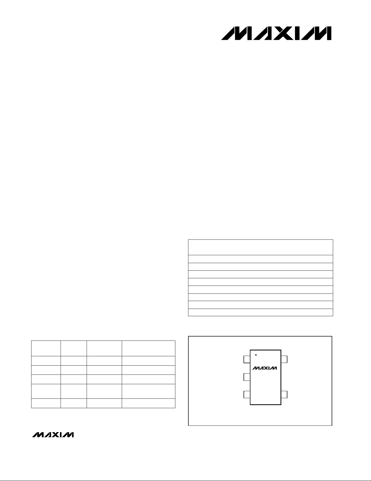
MAX4240
SOT23-5
TOP VIEW
2
34
_________________Pin Configurations
19-1343; Rev 0; 3/98
PART
MAX4240EUK-T
MAX4241EUA
MAX4241ESA -40°C to +85°C
-40°C to +85°C
-40°C to +85°C
TEMP. RANGE
PIN-
PACKAGE
5 SOT23-5
8 µMAX
8 SO
_______________Ordering Information
Pin Configurations continued at end of data sheet.
_____________________Selector Guide
NO. OF
AMPS
PIN-PACKAGE
MAX4240 1 5-pin SOT23
MAX4241 1 8-pin µMAX/SO
PART
MAX4242 2 8-pin µMAX/SO
SHUTDOWN
—
Yes
—
MAX4243 2
10-pin µMAX,
14-pin SO
MAX4244 4 14-pin SO
Yes
—
Beyond-the-Rails is a trademark of Maxim Integrated Products.
Rail-to-Rail is a registered trademark of Nippon Motorola Ltd.
MAX4242EUA
MAX4242ESA
MAX4243EUB
-40°C to +85°C
-40°C to +85°C
-40°C to +85°C 8 µMAX
8 SO
10 µMAX
MAX4243ESD
MAX4244ESD
-40°C to +85°C
-40°C to +85°C 14 SO
14 SO
SOT
TOP MARK
ACCS
—
—
—
—
—
—
—
Page 2
MAX4240–MAX4244
Single/Dual/Quad, +1.8V/10µA, SOT23,
Beyond-the-Rails Op Amps
2 _______________________________________________________________________________________
ABSOLUTE MAXIMUM RATINGS
ELECTRICAL CHARACTERISTICS — T
A
= +25°C
(VCC= +1.8V to +5.5V, VEE= 0, VCM= 0, V
OUT
= VCC/ 2, RL= 100kΩ tied to VCC/ 2, SHDN = VCC, TA= +25°C, unless
otherwise noted.) (Note 1)
Stresses beyond those listed under “Absolute Maximum Ratings” may cause permanent damage to the device. These are stress ratings only, and functional
operation of the device at these or any other conditions beyond those indicated in the operational sections of the specifications is not implied. Exposure to
absolute maximum rating conditions for extended periods may affect device reliability.
Supply Voltage (VCCto VEE)....................................................6V
All Other Pins ...................................(V
CC
+ 0.3V) to (VEE- 0.3V)
Output Short-Circuit Duration (to V
CC
or VEE)............Continuous
Continuous Power Dissipation (T
A
= +70°C)
5-pin SOT23 (derate 7.1mW/°C above +70°C).............571mW
8-pin µMAX (derate 4.1mW/°C above +70°C)..............330mW
8-pin SO (derate 5.88mW/°C above +70°C).................471mW
10-pin µMAX (derate 5.6mW/°C above +70°C)............444mW
14-pin SO (derate 8.33mW/°C above +70°C)...............667mW
Operating Temperature Range ...........................-40°C to +85°C
Junction Temperature......................................................+150°C
Storage Temperature Range.............................-65°C to +160°C
Lead Temperature (soldering, 10sec).............................+300°C
PARAMETER SYMBOL MIN TYP MAX UNITS
Input Bias Current I
B
±2 ±6 nA
CONDITIONS
Input Offset Voltage V
OS
±0.20 ±0.75
mV
MAX4241ESA
(VEE- 0.2V) ≤ VCM≤
(VCC+ 0.2V)
±0.25 ±1.40
MAX4240EUK/MAX424_EUA/
MAX4243EUB
±0.20 ±0.88
MAX4242ESA/MAX4243ESD/
MAX4244ESD
Supply Current
per Amplifier
I
CC
10 12
µA
VCC= 1.8V
SHDN = V
CC
14 18VCC= 5.0V
2.0 3.0VCC= 5.0V
Shutdown Supply
Current (Note 2)
I
CC(SHDN)
1.0 1.5
µA
VCC= 1.8V
SHDN = V
EE
Supply-Voltage Range V
CC
1.8 5.5 VInferred from PSRR test
(Note 3)
(Note 3)Input Offset Current I
OS
±0.5 ±1.5 nA
V
IN+
- V
IN-
< 1.0V
Differential Input
Resistance
R
IN(DIFF)
45 MΩ
V
IN+
- V
IN-
> 2.5V
4.4 kΩ
Inferred from the CMRR test
Input Common-Mode
Voltage Range
V
CM
VEE- 0.2 VCC+ 0.2 V
VCC= 1.8V
Common-Mode
Rejection Ratio
(Note 4)
CMRR
72 90
dB
MAX4241ESA
72 90
MAX4242ESA/MAX4243ESD/
MAX4244ESD
66 88
MAX4240EUK/MAX424_EUA/
MAX4243EUB
VCC= 5.0V
77 94MAX4241ESA
77 94
MAX4242ESA/MAX4243ESD/
MAX4244ESD
72 90
MAX4240EUK/MAX424_EUA/
MAX4243EUB
Page 3
Single/Dual/Quad, +1.8V/10µA, SOT23,
Beyond-the-Rails Op Amps
_______________________________________________________________________________________ 3
ELECTRICAL CHARACTERISTICS — TA= +25°C (continued)
(VCC= +1.8V to +5.5V, VEE= 0, VCM= 0, V
OUT
= VCC/ 2, RL= 100kΩ tied to VCC/ 2, SHDN = VCC, TA= +25°C, unless
otherwise noted.) (Note 1)
Channel-to-Channel
Isolation (Note 6)
CH
ISO
80 dBSpecified at DC
Phase Margin
Φ
m
68 degrees
Gain Margin G
m
18 dB
Slew Rate SR 40 V/ms
SHDN Input Bias
Current (Note 2)
IIH, I
IL
40 80 nA
SHDN = VCC= 5.5V or SHDN = VEE= 0
SHDN Logic Low
(Note 2)
V
IL
0.3 x V
CC
V
6 15
PARAMETER SYMBOL MIN TYP MAX UNITS
23 35
Specified as
VEE- VOL
Output Voltage
Swing Low
10 20
V
OL
40 60
mV
VCC= 5.0V
RL= 10kΩ
RL= 100kΩ
RL= 100kΩ
VCC= 1.8V
RL= 10kΩ
8 20
40 65
Specified as
VCC- VOH
Output Voltage
Swing High
10 25
80 85
V
OH
70 73
60 95
mV
VCC= 5.0V
RL= 10kΩ
2.5
mA
SHDN Logic High
(Note 2)
V
IH
0.7 x V
CC
V
(VEE+ 0.2V) ≤ V
OUT
≤
(VCC- 0.2V)
Large-Signal
Voltage Gain
90 94
A
VOL
82 85
dB
RL= 100kΩ
RL= 100kΩ
CONDITIONS
Sinking
VCC= 1.8V
RL= 10kΩ
VCC= 5.0V
RL= 10kΩ
RL= 100kΩ
RL= 100kΩ
RL= 10kΩ
VCC= 1.8V
Gain-Bandwidth
Product
GBW 90 kHz
Power-Supply
Rejection Ratio
PSRR
80 85
dB
MAX4241ESA
1.8V ≤ VCC≤ 5.5V
MAX4240–MAX4244
78 82
MAX4240EUK/MAX424_EUA/
MAX4243EUB
80 85
MAX4242ESA/MAX4243ESD/
MAX4244ESD
Output Leakage
Current in Shutdown
(Notes 2, 5)
I
OUT(SHDN)
20 50 nA
SHDN = VEE= 0, VCC= 5.5V
Output Short-Circuit
Current
I
OUT(SC)
Sourcing 0.7
Page 4
MAX4240–MAX4244
Single/Dual/Quad, +1.8V/10µA, SOT23,
Beyond-the-Rails Op Amps
4 _______________________________________________________________________________________
Enable Time from
Shutdown
t
ENABLE
150
Input Voltage Noise
Density
e
n
70
nV/√Hz
Input Current Noise
Density
i
n
0.05
pA/√Hz
Capacitive-Load
Stability
200 pF
Shutdown Time t
SHDN
50 µs
µs
Power-Up Time t
ON
200 µs
Input Capacitance C
IN
3 pF
f = 1kHz
f = 1kHz
A
VCL
= +1V/V, no sustained oscillations
PARAMETER SYMBOL MIN TYP MAX UNITS
Total Harmonic
Distortion
THD 0.05 %
Settling Time to 0.01% t
S
CONDITIONS
50 µs
fIN= 1kHz, VCC= 5.0V, V
OUT
= 2Vp-p, AV= +1V/V
AV= +1V/V, VCC= 5.0V, V
OUT
= 2V
STEP
ELECTRICAL CHARACTERISTICS — TA= +25°C (continued)
(VCC= +1.8V to +5.5V, VEE= 0, VCM= 0, V
OUT
= VCC/ 2, RL= 100kΩ tied to VCC/ 2, SHDN = VCC, TA= +25°C, unless
otherwise noted.) (Note 1)
ELECTRICAL CHARACTERISTICS — TA= T
MIN
to
T
MAX
(VCC= +1.8V to +5.5V, VEE= 0, VCM= 0, V
OUT
= VCC/ 2, RL= 100kΩ tied to VCC/ 2, SHDN = VCC, TA= T
MIN
to T
MAX
, unless oth-
erwise noted.) (Note 1)
SHDN = V
CC
±1.2
Inferred from PSRR test
Inferred from the CMRR test
(Note 3)
CONDITIONS
MAX4241ESA
(VEE- 0.2V) ≤ VCM≤
(VCC+ 0.2V)
mVV
OS
Input Offset Voltage
µA
19
I
CC
SHDN = V
EE
14
V1.8 5.5V
CC
Supply-Voltage Range
Supply Current
per Amplifier
V-0.2 VCC+ 0.2V
CM
Input Common-Mode
Voltage Range
µV/°C2TC
VOS
Input Offset Voltage
Drift
nA±7I
OS
Input Offset Current
UNITSMIN TYP MAXSYMBOLPARAMETER
µA
3.5
I
CC(SHDN)
2.0
Shutdown Supply
Current (Note 2)
VCC= 1.8V
VCC= 5.0V
VCC= 1.8V
VCC= 5.0V
(Note 3) nA±15I
B
Input Bias Current
±1.3
MAX4242ESA/MAX4243ESD/
MAX4244ESD
±2.0
MAX4240EUK/MAX424_EUA/
MAX4243EUB
Page 5
MAX4240–MAX4244
Single/Dual/Quad, +1.8V/10µA, SOT23,
Beyond-the-Rails Op Amps
_______________________________________________________________________________________ 5
ELECTRICAL CHARACTERISTICS — TA= T
MIN
to
T
MAX
(continued)
(VCC= +1.8V to +5.5V, VEE= 0, VCM= 0, V
OUT
= VCC/ 2, RL= 100kΩ tied to VCC/ 2, SHDN = VCC, TA= T
MIN
to T
MAX
, unless oth-
erwise noted.) (Note 1)
68
MAX4242ESA/MAX4243ESD/
MAX4244ESD
68
SHDN = V
EE
= 0, VCC= 5.5V
RL= 10kΩ
64
CONDITIONS
MAX4240EUK/MAX424_EUA/
MAX4243EUB
MAX4241ESA
VCC= 1.8V
dBCMRR
Common-Mode
Rejection Ratio
(Note 4)
nA100I
OUT(SHDN)
Output Leakage
Current in Shutdown
(Notes 2, 5)
76
UNITSMIN TYP MAXSYMBOLPARAMETER
RL= 100kΩ
dB
76
A
VOL
Large-Signal
Voltage Gain
74
MAX4242ESA/MAX4243ESD/
MAX4244ESD
74
70
MAX4240EUK/MAX424_EUA/
MAX4243EUB
MAX4241ESA
VCC= 5.0V
76
MAX4242ESA/MAX4243ESD/
MAX4244ESD
76
74
MAX4240EUK/MAX424_EUA/
MAX4243EUB
MAX4241ESA
1.8V ≤ VCC≤ 5.5V dBPSRR
Power-Supply
Rejection Ratio
RL= 100kΩ 84
RL= 10kΩ 66
(VEE+ 0.2V) ≤ V
OUT
≤
(VCC- 0.2V)
VCC= 1.8V
VCC= 5.0V
RL= 100kΩ
dB
25
V
OH
Output Voltage
Swing High
RL= 100kΩ 30
RL= 10kΩ
VCC= 1.8V
RL= 10kΩ 95
VCC= 5.0V
Specified as
VCC- VOH
145
RL= 100kΩ
dB
20
V
OL
Output Voltage
Swing Low
RL= 100kΩ 25
RL= 10kΩ
VCC= 1.8V
RL= 10kΩ 50
VCC= 5.0V
Specified as
V
EE
- VOL
75
V0.3 x V
CC
V
IL
SHDN Logic Low
(Note 2)
Page 6

MAX4240–MAX4244
Single/Dual/Quad, +1.8V/10µA, SOT23,
Beyond-the-Rails Op Amps
6 _______________________________________________________________________________________
ELECTRICAL CHARACTERISTICS — TA= T
MIN
to T
MAX
(continued)
(VCC= +1.8V to +5.5V, VEE= 0, VCM= 0, V
OUT
= VCC/ 2, RL= 100kΩ tied to VCC/ 2, SHDN = VCC, TA= T
MIN
to T
MAX
, unless oth-
erwise noted.) (Note 1)
Note 1: The MAX4240EUK, MAX4241EUA, MAX4242EUA, and MAX4243EUB specifications are 100% tested at T
A
= +25°C. All
temperature limits are guaranteed by design.
Note 2: Shutdown mode applies to the MAX4241/MAX4243 only.
Note 3: Input bias current and input offset current are tested with V
CC
= +5.0V and 0 ≤ VCM≤ 5.0V.
Note 4: Tested over the specified input common-mode range.
Note 5: Tested for 0 ≤ V
OUT
≤ VCC. Does not include current through external feedback network.
Note 6: Channel-to-channel isolation specification applies to the MAX4242/MAX4243/MAX4244 only.
SHDN Logic High
(Note 2)
V
IH
0.7 x V
CC
V
SHDN Input Bias
Current (Note 2)
IIH, I
IL
120 nA
SHDN = VCC= 5.5V or SHDN = VEE= 0
PARAMETER SYMBOL MIN TYP MAX UNITSCONDITIONS
20
0
-60 -40 -20 20
40
100
SUPPLY CURRENT PER AMPLIFIER
vs. TEMPERATURE
6
4
2
16
14
18
MAX4240/44-01
TEMPERATURE (°C)
SUPPLY CURRENT (µA)
0 60
10
8
12
80
VCC = +5.5V
VCC = +1.8V
5
0
-60 -40 -20
0
20 40 100
SHUTDOWN SUPPLY CURRENT
PER AMPLIFIER vs. TEMPERATURE
1
4
MAX4240/44-02
TEMPERATURE (°C)
SHUTDOWN SUPPLY CURRENT (µA)
60
2
3
80
VCC = +5.5V
VCC = +1.8V
1.8
1.0
-60 -40 -20 20
40
100
MINIMUM OPERATING VOLTAGE
vs. TEMPERATURE
1.2
1.1
1.6
1.7
MAX4240/44-03
TEMPERATURE (°C)
V
CC
(V)
0 60
1.4
1.3
1.5
80
PSRR ≥ 80dB
__________________________________________Typical Operating Characteristics
(VCC= +5.0V, VEE= 0, VCM= V
CC
/ 2, V
SHDN
= VCC, RL= 100kΩ to V
CC
/ 2, TA= +25°C, unless otherwise noted.)
400
0
-60 -40 -20 20
40
100
INPUT OFFSET VOLTAGE
vs. TEMPERATURE
100
300
MAX4240/44-04
TEMPERATURE (°C)
INPUT OFFSET VOLTAGE (µV)
0 60
200
80
0
-4
-60 -40 -20 20
40
100
INPUT BIAS CURRENT
vs. TEMPERATURE
-3
-1
MAX4240/44-05
TEMPERATURE (°C)
INPUT BIAS CURRENT (nA)
0 60-280
VCM = 0
VCC = +1.8V
VCC = +5.5V
5.0
-5.0
-0.2 0.2 0.6 1.0 1.4
INPUT BIAS CURRENT vs.
COMMON-MODE VOLTAGE (V
CC
= 1.8V)
-2.5
2.5
MAX4240/44-06a
VCM (V)
I
BIAS
(nA)
0
1.8
V
CC
= +1.8V
Page 7
MAX4240–MAX4244
Single/Dual/Quad, +1.8V/10µA, SOT23,
Beyond-the-Rails Op Amps
_______________________________________________________________________________________
7
5.0
-5.0
-0.5 0.5
1.5
2.5 3.5
4.5
INPUT BIAS CURRENT vs.
COMMON-MODE VOLTAGE (V
CC
= 5.5V)
-2.5
2.5
MAX4240/44-06b
VCM (V)
I
BIAS
(nA)
0
5.5
V
CC
= +5.5V
120
0
-60 -40 -20 20
40
100
OUTPUT SWING HIGH
vs. TEMPERATURE
20
100
80
MAX4240/44-07
TEMPERATURE (°C)
VOLTAGE FROM V
CC
(mV)
0 60
60
40
80
VCC = +1.8V, RL = 10kΩ
RL TO V
EE
VCC = +5.5V, RL = 20kΩ
VCC = +5.5V, RL = 100kΩ
VCC = +1.8V, RL = 100kΩ
120
0
-60 -40 -20 20
40
100
OUTPUT SWING LOW
vs. TEMPERATURE
20
100
80
MAX4240/44-08
TEMPERATURE (°C)
VOLTAGE FROM V
EE
(mV)
0 60
60
40
80
VCC = +1.8V, RL = 10kΩ
VCC = +5.5V, RL = 20kΩ
VCC = +5.5V, RL = 100kΩ
VCC = +1.8V, RL = 100kΩ
RL TO V
CC
-80
-100
-60 -40 -20 20
40
100
COMMON-MODE REJECTION
vs. TEMPERATURE
-95
-85
MAX4240/44-09
TEMPERATURE (°C)
COMMON-MODE REJECTION (dB)
0 60
-90
80
VCC = +1.8V
VCC = +5.5V
100
110
0 100 200 300 400
OPEN-LOOP GAIN vs. OUTPUT SWING LOW
(V
CC
= +5.5V, RL TIED TO VEE)
50
40
90
80
MAX4240/44-12
∆V
OUT
(mV)
GAIN (dB)
70
60
RL = 100kΩ
RL = 20kΩ
100
30
0 100 300 500
OPEN-LOOP GAIN vs. OUTPUT SWING LOW
(V
CC
= +1.8V, RL TIED TO VEE)
50
40
90
80
MAX4240/44-10
∆V
OUT
(mV)
GAIN (dB)
200 400
70
60
RL = 100kΩ
RL = 10kΩ
100
30
0 100 300 500
OPEN-LOOP GAIN vs. OUTPUT SWING HIGH
(V
CC
= +1.8V, RL TIED TO VEE)
50
40
90
80
MAX4240/44-11
∆V
OUT
(mV)
GAIN (dB)
200 400
70
60
RL = 100kΩ
RL = 10kΩ
100
110
0 100 200 300 400
OPEN-LOOP GAIN vs. OUTPUT SWING HIGH
(V
CC
= +5.5V, RL TIED TO VEE)
50
40
90
80
MAX4240/44-13
∆V
OUT
(mV)
GAIN (dB)
70
60
RL = 20kΩ
RL = 100kΩ
110
70
-60 -40 -20 20
40
100
OPEN-LOOP GAIN
vs. TEMPERATURE
75
80
105
100
95
MAX4240/44-14
TEMPERATURE (°C)
GAIN (dB)
0 60
90
85
80
VCC = +5.5V, RL = 20kΩ TO V
CC
VCC = +5.5V, RL = 20kΩ TO V
EE
VCC = +1.8V, RL = 10kΩ TO V
EE
VCC = +1.8V, RL = 10kΩ TO V
CC
____________________________________Typical Operating Characteristics (continued)
(VCC= +5.0V, VEE= 0, VCM= V
CC
/ 2, V
SHDN
= VCC, RL= 100kΩ to V
CC
/ 2, TA= +25°C, unless otherwise noted.)
Page 8

MAX4240–MAX4244
Single/Dual/Quad, +1.8V/10µA, SOT23,
Beyond-the-Rails Op Amps
8 _______________________________________________________________________________________
____________________________________Typical Operating Characteristics (continued)
(VCC= +5.0V, VEE= 0, VCM= V
CC
/ 2, V
SHDN
= VCC, RL= 100kΩ to V
CC
/ 2, TA= +25°C, unless otherwise noted.)
110
70
-60 -40 -20 20
40
100
OPEN-LOOP GAIN
vs. TEMPERATURE
75
80
105
100
95
MAX4240/44-15
TEMPERATURE (°C)
GAIN (dB)
0 60
90
85
80
VCC = +5.5V, RL TO V
CC
VCC = +5.5V, RL TO V
EE
VCC = +1.8V, RL TO V
CC
VCC = +1.8V, RL TO V
EE
60
-40
10 100 1k 10k 100k
GAIN AND PHASE vs. FREQUENCY
(C
L
= 0pF)
-20
-30
MAX4240/44-16
FREQUENCY (Hz)
GAIN (dB)
0
-10
20
10
30
40
50
180
-180
-108
-144
PHASE (DEGREES)
-36
-72
36
0
72
108
144
AV = +1000V/V
60
-40
10 100 1k 10k 100k
GAIN AND PHASE vs. FREQUENCY
(C
L
= 100pF)
-20
-30
MAX4240/44-17
FREQUENCY (Hz)
GAIN (dB)
0
-10
20
10
30
40
50
180
-180
-108
-144
PHASE (DEGREES)
-36
-72
36
0
72
108
144
AV = +1000V/V
-60
-110
10 1k 10k
100
MAX4242/MAX4243/MAX4244
CROSSTALK vs. FREQUENCY
-100
MAX4240/44-18
FREQUENCY (Hz)
GAIN (dB)
-90
-80
-70
RL = 10kΩ
1
0.01
1 100010010
TOTAL HARMONIC DISTORTION PLUS NOISE
vs. FREQUENCY
0.1
MAX4240/44-19
FREQUENCY (Hz)
THD + NOISE (%)
RL = 10kΩ
RL = 100kΩ
1000
10
0 250 500 1000
LOAD RESISTOR vs.
CAPACITIVE LOAD
MAX4240/44-20
C
LOAD
(pF)
R
LOAD
(kΩ)
750
100
10%
OVERSHOOT
REGION OF
MARGINAL STABILITY
REGION OF
STABLE OPERATION
10µs/div
SMALL-SIGNAL TRANSIENT RESPONSE
(NONINVERTING)
MAX4240/44-21
50mV/div
100mV
100mV
IN
OUT
0V
0V
10µs/div
SMALL-SIGNAL TRANSIENT RESPONSE
(INVERTING)
MAX4240/44-22
50mV/div
100mV
100mV
IN
OUT
0V
0V
Page 9

MAX4240–MAX4244
Single/Dual/Quad, +1.8V/10µA, SOT23,
Beyond-the-Rails Op Amps
_______________________________________________________________________________________ 9
______________________________________________________________Pin Description
Amplifier Output. High impedance when in
shutdown mode.
OUT1 6 —— — —
4 44 4 11
Negative Supply. Tie to ground for singlesupply operation.
V
EE
2
3 —— — —
2 —— — — Inverting InputIN-4
Noninverting InputIN+3
7 108 14 4
1, 5 ——
5, 7,
8, 10
— No Connection. Not internally connected.N.C.—
8 —
Positive SupplyV
CC
5
— — —
— 1, 91, 7 1, 13 1, 7
Outputs for Amplifiers A and B. High impedance when in shutdown mode.
OUTA,
OUTB
—
Shutdown Input. Drive high, or tie to VCCfor
normal operation. Drive to VEEto place device
in shutdown mode.
SHDN
—
— 2, 82, 6 2, 12 2, 6
— 3, 73, 5 3, 11 3, 5 Noninverting Inputs to Amplifiers A and B
INA+,
INB+
—
— 5, 6
Inverting Inputs to Amplifiers A and B
INA-,
INB-
—
— 6, 9 —
— —— — 8, 14 Outputs for Amplifiers C and D
OUTC,
OUTD
—
Shutdown Inputs for Amplifiers A and B. Drive
high, or tie to VCCfor normal operation. Drive
to VEEto place device in shutdown mode.
SHDNA,
SHDNB
—
— —— — 9, 13
— —— — 10, 12 Noninverting Inputs to Amplifiers C and D
INC+,
IND+
—
Inverting Inputs to Amplifiers C and D
INC-,
IND-
—
PIN
MAX4243
MAX4244MAX4241
µMAX
MAX4242
SO
MAX4240
FUNCTIONNAME
____________________________________Typical Operating Characteristics (continued)
(VCC= +5.0V, VEE= 0, VCM= V
CC
/ 2, V
SHDN
= VCC, RL= 100kΩ to V
CC
/ 2, TA= +25°C, unless otherwise noted.)
100µs/div
LARGE-SIGNAL TRANSIENT RESPONSE
(INVERTING)
MAX4240/44-24
2V/div
+2V
-2V
-2V
+2V
IN
OUT
LARGE-SIGNAL TRANSIENT RESPONSE
(NONINVERTING)
IN
2V/div
OUT
100µs/div
MAX4240/44-23
4.5V
0.5V
4.5V
0.5V
Page 10

MAX4240–MAX4244
Single/Dual/Quad, +1.8V/10µA, SOT23,
Beyond-the-Rails Op Amps
10 ______________________________________________________________________________________
_______________Detailed Description
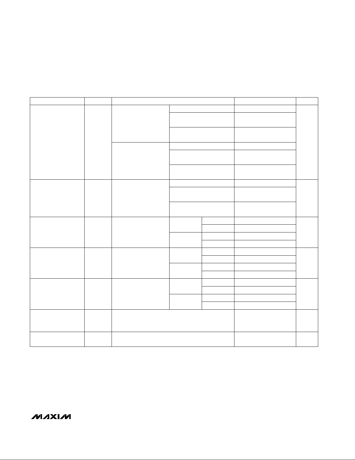
Beyond-the-Rails Input Stage
The MAX4240–MAX4244 have Beyond-the-Rails™ inputs
and Rail-to-Rail®output stages that are specifically
designed for low-voltage, single-supply operation. The
input stage consists of separate NPN and PNP differential stages, which operate together to provide a common-mode range extending to 200mV beyond both
supply rails. The crossover region of these two pairs
occurs halfway between VCCand VEE. The input offset
voltage is typically 200µV. Low operating supply voltage,
low supply current, beyond-the-rails common-mode
input range, and rail-to-rail outputs make this family of
operational amplifiers an excellent choice for precision or
general-purpose, low-voltage battery-powered systems.
Since the input stage consists of NPN and PNP pairs,
the input bias current changes polarity as the commonmode voltage passes through the crossover region.
Match the effective impedance seen by each input to
reduce the offset error caused by input bias currents
flowing through external source impedances (Figures
1a and 1b). The combination of high source impedance
plus input capacitance (amplifier input capacitance
plus stray capacitance) creates a parasitic pole that
produces an underdamped signal response. Reducing
input capacitance or placing a small capacitor across
the feedback resistor improves response in this case.
The MAX4240–MAX4244 family’s inputs are protected
from large differential input voltages by internal 2.2kΩ
series resistors and back-to-back triple-diode stacks
across the inputs (Figure 2). For differential input voltages (much less than 1.8V), input resistance is typically
45MΩ. For differential input voltages greater than 1.8V,
input resistance is around 4.4kΩ, and the input bias
current can be approximated by the following equation:
I
BIAS
= (V
DIFF
- 1.8V) / 4.4kΩ
R3
V
IN
R3 = R1 R2
R1 R2
MAX4240
MAX4241
MAX4242
MAX4243
MAX4244
Figure 1a. Minimizing Offset Error Due to Input Bias Current
(Noninverting)
R3
R3 = R1 R2
R1 R2
MAX4240
MAX4241
MAX4242
MAX4243
MAX4244
V
IN
Figure 1b. Minimizing Offset Error Due to Input Bias Current
(Inverting)
2.2k
2.2k
IN-
IN+
Figure 2. Input Protection Circuit
Page 11
In the region where the differential input voltage
approaches 1.8V, the input resistance decreases exponentially from 45MΩ to 4.4kΩ as the diode block begins
conducting. Conversely, the bias current increases with
the same curve.
Rail-to-Rail Output Stage
The MAX4240–MAX4244 output stage can drive up to a
10kΩ load and still swing to within 40mV of the rails.
Figure 3 shows the output voltage swing of a MAX4240
configured as a unity-gain buffer, powered from a single
+2V supply voltage. The output for this setup typically
swings from (VEE+ 6mV) to (VCC- 8mV) with a 100kΩ
load.
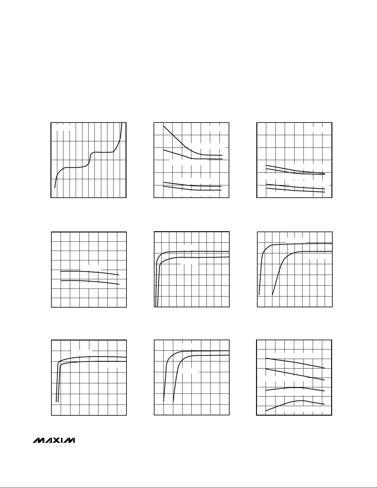
__________Applications Information
Power-Supply Considerations
The MAX4240–MAX4244 operate from a single +1.8V
to +5.5V supply (or dual ±0.9V to ±2.75V supplies) and
consume only 10µA of supply current per amplifier. A
high power-supply rejection ratio of 90dB allows the
amplifiers to be powered directly off a decaying battery
voltage, simplifying design and extending battery life.
The MAX4240–MAX4244 are ideally suited for use with
most battery-powered systems. Table 1 lists a variety of
typical battery types showing voltage when fresh, voltage at end-of-life, capacity, and approximate operating
time from a MAX4240/MAX4241, assuming nominal
conditions for both normal and shutdown modes.
Although the amplifiers are fully guaranteed over temperature for operation down to a +1.8V single supply,
even lower-voltage operation is possible in practice.
Figures 4 and 5 show the PSRR and supply current as
a function of supply voltage and temperature.
Power-Up Settling Time
The MAX4240–MAX4244 typically require 200µs to
power up after VCCis stable. During this start-up time,
the output is indeterminant. The application circuit
should allow for this initial delay.
Shutdown Mode
The MAX4241 (single) and MAX4243 (dual) feature a
low-power shutdown mode. When the shutdown pin
(SHDN) is pulled low, the supply current drops to 1µA
per amplifier, the amplifier is disabled, and the outputs
enter a high-impedance state. Pulling SHDN high or
leaving it floating enables the amplifier. Take care to
ensure that parasitic leakage current at the SHDN pin
does not inadvertently place the part into shutdown
mode when SHDN is left floating. Figure 6 shows the
output voltage response to a shutdown pulse. The logic
threshold for SHDN is always referred to VCC/ 2 (not to
MAX4240–MAX4244
Single/Dual/Quad, +1.8V/10µA, SOT23,
Beyond-the-Rails Op Amps
______________________________________________________________________________________ 11
1V/div
OUT
IN
1V/div
MAX4240-44 fig03
200µs/div
RL = 100kΩ TIED TO V
EE
VIN = 2.0V
f
IN
= 1kHz
Figure 3. Rail-to-Rail Input/Output Voltage Range
100
60
1.0 1.2 2.0
70
90
MAX4240-44 fig04
SUPPLY VOLTAGE (V)
PSRR (dB)
1.4 1.6801.8
TA = +85°C
TA = +25°C
TA = -40°C
Figure 4. Power-Supply Rejection Ratio vs. Supply Voltage
12
0
1.0 1.2 2.0
2
4
10
MAX4240-44 fig05
SUPPLY VOLTAGE (V)
SUPPLY CURRENT (µA)
1.4 1.6
6
8
1.8
TA = +85°C
TA = +25°C
TA = -40°C
Figure 5. Supply Current vs. Supply Voltage
Page 12

MAX4240–MAX4244
GND). When using dual supplies, pull SHDN to VEEto
enter shutdown mode.
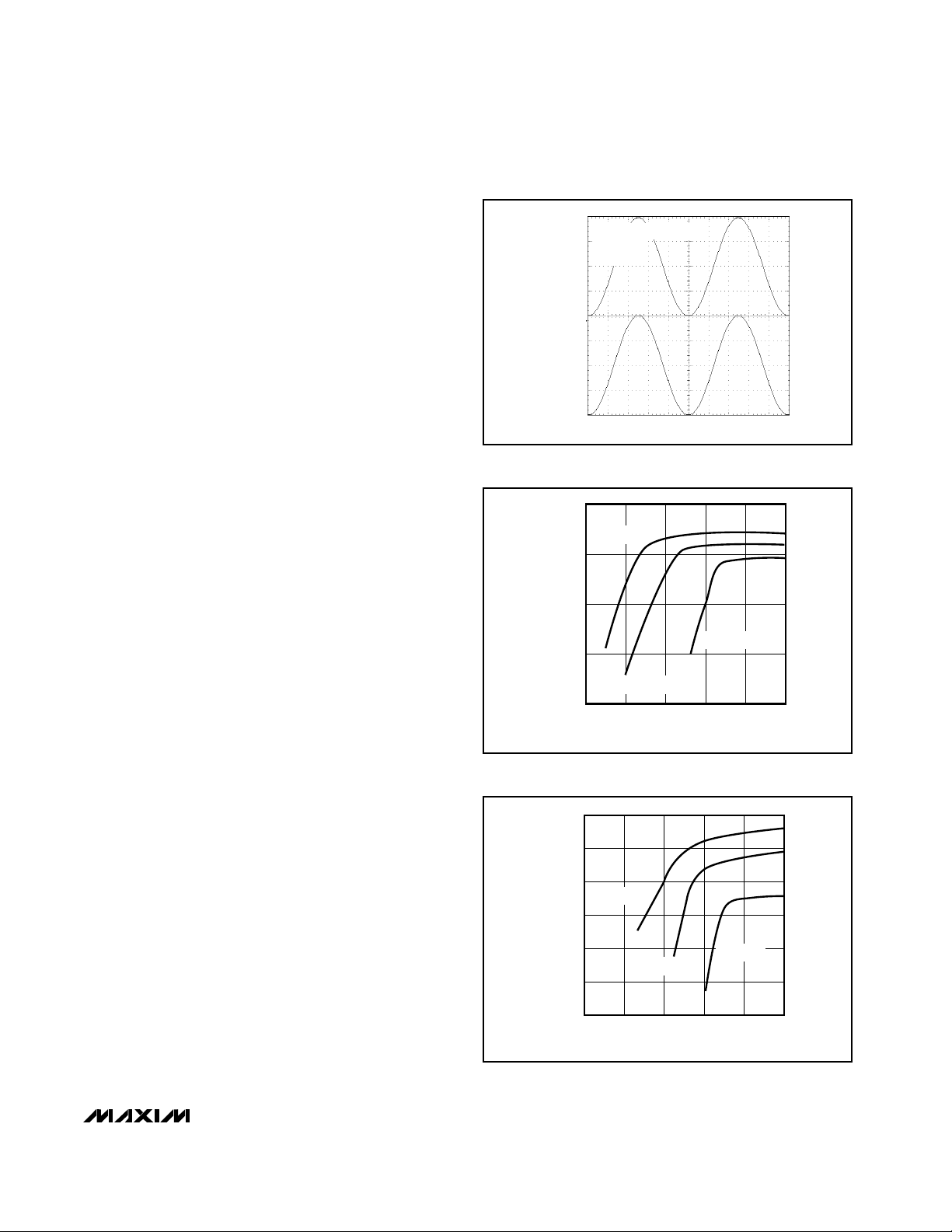
Load-Driving Capability
The MAX4240–MAX4244 are fully guaranteed over temperature and supply voltage to drive a maximum resistive load of 10kΩ to VCC/ 2, although heavier loads can
be driven in many applications. The rail-to-rail output
stage of the amplifier can be modeled as a current
source when driving the load toward VCC, and as a current sink when driving the load toward VEE. The magnitude of this current source/sink varies with supply
voltage, ambient temperature, and lot-to-lot variations
of the units.
Figures 7a and 7b show the typical current source and
sink capability of the MAX4240–MAX4244 family as a
function of supply voltage and ambient temperature.
The contours on the graph depict the output current
Single/Dual/Quad, +1.8V/10µA, SOT23,
Beyond-the-Rails Op Amps
12 ______________________________________________________________________________________
MAX4240-44 fig06
200µs/div
5V/div
1V/div
SHDN
OUT
VIN = 2V
R
L
= 100kΩ TIED TO V
EE
Figure 6. Shutdown Enable/Disable Output Voltage
1200
0
-60 -40 -20 100
200
400
1000
MAX4240-44 fig07a
TEMPERATURE (°C)
OUTPUT SOURCE CURRENT (µA)
0 4020
600
800
8060
VCC = 5.5V, VOH = 200mV
VCC = 5.5V, VOH = 100mV
VCC = 1.8V, VOH = 50mV
VCC = 5.5V, VOH = 50mV
VCC = 1.8V,
V
OH
= 200mV
V
CC
= 1.8V,
V
OH
= 100mV
Figure 7a. Output Source Current vs. Temperature
3000
0
-60 -40 -20 100
500
1000
2500
MAX4240-44 fig07b
TEMPERATURE (°C)
OUTPUT SINK CURRENT (µA)
0 4020
1500
2000
8060
VCC = 5.5V, VOL = 200mV
VCC = 1.8V, VOL = 200mV
VCC = 5.5V,
V
OL
= 100mV
VCC = 1.8V, VOL = 50mV
VCC = 5.5V, VOL = 50mV
VCC = 1.8V, VOL = 100mV
Figure 7b. Output Sink Current vs. Temperature
Table 1. MAX4240/MAX4241 Characteristics with Typical Battery Systems
RECHARGEABLE
V
END-OF-LIFE
(V)
Alkaline (2 Cells) No 3.0
Nickel-
Cadmium (2 Cells)
Yes
1.8
BATTERY TYPE
Lithium-Ion (1 Cell) Yes
2.4
Nickel-MetalHydride (2 Cells)
Yes
1.8
V
FRESH
(V)
3.5 2.7
2.4 1.8
CAPACITY,
AA SIZE
(mA-h)
2000
750
1000
1000
MAX4240/MAX4241
OPERATING TIME
IN NORMAL MODE
(Hours)
200,000
75,000
100,000
100,000
MAX4241
OPERATING TIME
IN SHUTDOWN
MODE (Hours)
2 x 10
6
0.75 x 10
6
10
6
10
6
Page 13

value, based on driving the output voltage to within
50mV, 100mV, and 200mV of either power-supply rail.
For example, a MAX4241 running from a single +1.8V
supply, operating at TA= +25°C, can source 240µA to
within 100mV of VCCand is capable of driving a 7kΩ
load resistor to VEE:
The same application can drive a 3.3kΩ load resistor
when terminated in VCC/ 2 (+0.9V in this case).
Driving Capacitive Loads
The MAX4240–MAX4244 are unity-gain stable for loads
up to 200pF (see Load Resistor vs. Capacitive Load
graph in
Typical Operating Characteristics
). Applications that require greater capacitive drive capability
should use an isolation resistor between the output and
the capacitive load (Figure 8). Note that this alternative
results in a loss of gain accuracy because R
ISO
forms a
voltage divider with the load resistor.
Power-Supply Bypassing and Layout
The MAX4240–MAX4244 family operates from either a
single +1.8V to +5.5V supply or dual ±0.9V to ±2.75V
supplies. For single-supply operation, bypass the
power supply with a 100nF capacitor to VEE(in this
case GND). For dual-supply operation, both the V
CC
and VEEsupplies should be bypassed to ground with
separate 100nF capacitors.
Good PC board layout techniques optimize performance by decreasing the amount of stray capacitance
at the op amp’s inputs and output. To decrease stray
capacitance, minimize trace lengths by placing external components as close as possible to the op amp.
Surface-mount components are an excellent choice.
R =
1.8V - 0.1V
240 A
7k to V
L EE
µ
= Ω
MAX4240–MAX4244
Single/Dual/Quad, +1.8V/10µA, SOT23,
Beyond-the-Rails Op Amps
______________________________________________________________________________________ 13
R
ISO
C
L
R
L
MAX4240
MAX4241
MAX4242
MAX4243
MAX4244
AV =
R
L
≈ 1
R
L
+ R
ISO
Figure 8a Using a Resistor to Isolate a Capacitive Load from
the Op Amp
50mV/div
IN
OUT
50mV/div
MAX4240-44 fig08b
100µs/div
R
ISO
= NONE, RL = 100kΩ, CL = 700pF
Figure 8b. Pulse Response without Isolating Resistor
50mV/div
IN
OUT
50mV/div
MAX4240-44 fig08c
100µs/div
R
ISO
= 1kΩ, RL = 100kΩ, CL = 700pF
Figure 8c. Pulse Response with Isolating Resistor
Page 14

MAX4240–MAX4244
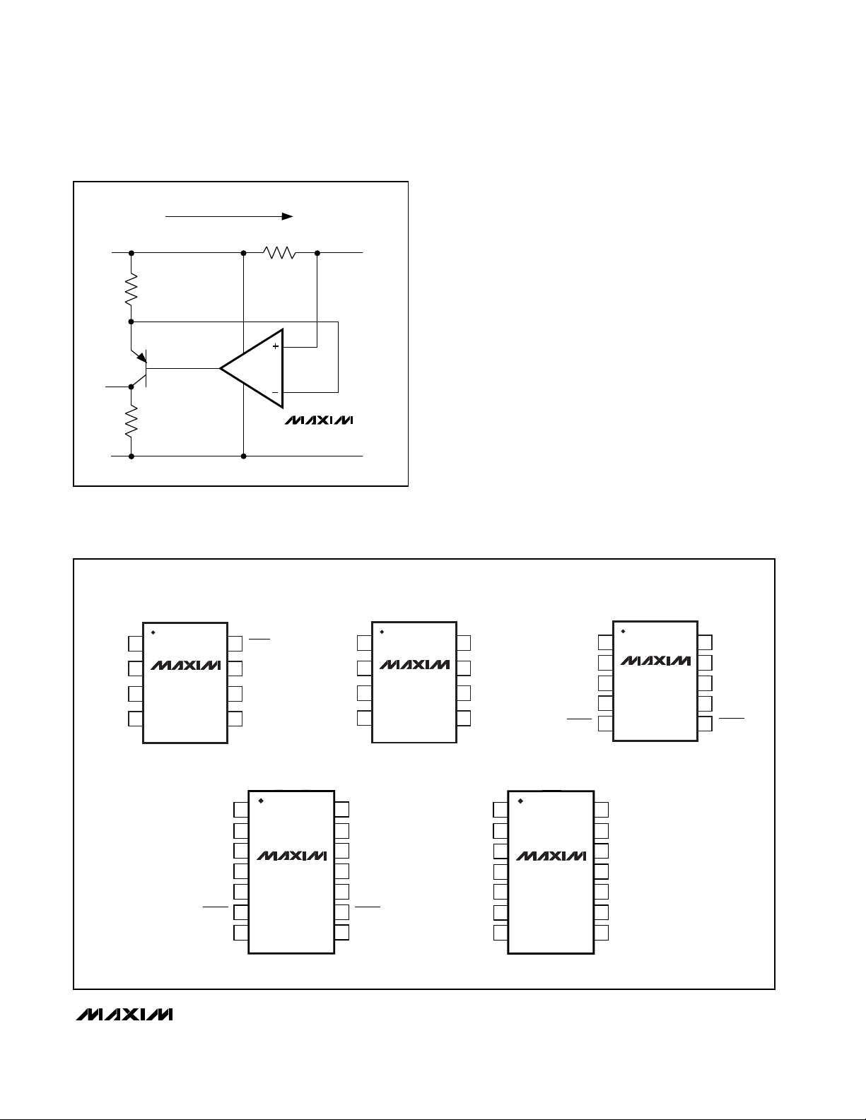
Using the MAX4240–MAX4244
as Comparators
Although optimized for use as operational amplifiers,
the MAX4240–MAX4244 can also be used as rail-to-rail
I/O comparators. Typical propagation delay depends
on the input overdrive voltage, as shown in Figure 9.
External hysteresis can be used to minimize the risk of
output oscillation. The positive feedback circuit, shown
in Figure 10, causes the input threshold to change
when the output voltage changes state. The two thresholds create a hysteresis band that can be calculated by
the following equations:
V
HYST
= VHI- V
LO
VLO= VINx R2 / (R1 + (R1 x R2 / R
HYST
) + R2)
VHI= [(R2 / R1 x VIN) + (R2 / R
HYST
) x VCC] /
(1 + R1 / R2 + R2 / R
HYST
)
The MAX4240–MAX4244 contain special circuitry to
boost internal drive currents to the amplifier output
stage. This maximizes the output voltage range over
which the amplifiers are linear. In an open-loop comparator application, the excursion of the output voltage
is so close to the supply rails that the output stage transistors will saturate, causing the quiescent current to
increase from the normal 10µA. Typical quiescent currents increase to 35µA for the output saturating at V
CC
and 28µA for the output at VEE.
Using the MAX4240–MAX4244
as Ultra-Low-Power Current Monitors
The MAX4240–MAX4244 are ideal for applications
powered from a 2-cell battery stack. Figure 11 shows
an application circuit in which the MAX4240 is used for
monitoring the current of a 2-cell battery stack. In this
circuit, a current load is applied, and the voltage drop
at the battery terminal is sensed.
The voltage on the load side of the battery stack is
equal to the voltage at the emitter of Q1, due to the
feedback loop containing the op amp. As the load current increases, the voltage drop across R1 and R2
increases. Thus, R2 provides a fraction of the load current (set by the ratio of R1 and R2) that flows into the
emitter of the PNP transistor. Neglecting PNP base current, this current flows into R3, producing a ground-referenced voltage proportional to the load current. Scale
R1 to give a voltage drop large enough in comparison
to VOSof the op amp, in order to minimize errors.
The output voltage of the application can be calculated
using the following equation:
V
OUT
= [I
LOAD
x (R1 / R2)] x R3
For a 1V output and a current load of 50mA, the choice
of resistors can be R1 = 2Ω, R2 = 100kΩ, R3 = 1MΩ.
The circuit consumes less power (but is more susceptible to noise) with higher values of R1, R2, and R3.
Single/Dual/Quad, +1.8V/10µA, SOT23,
Beyond-the-Rails Op Amps
14 ______________________________________________________________________________________
R2
R1
V
IN
OUTPUT
INPUT
V
OH
V
OL
V
EE
V
CC
V
OUT
R
HYST
V
EE
MAX4240
MAX4241
MAX4242
MAX4243
MAX4244
HYSTERESIS
V
LO
V
OH
V
HI
Figure 10. Hysteresis Comparator Circuit
10,000
10
0 20 3010 100
100
1000
MAX4240-44 fig09
V
OD
(mV)
t
PD
(µs)
40 50 60 70 80
90
tPD-; V
CC
= +5V
tPD+; V
CC
= +1.8V
tPD-; V
CC
= +1.8V
tPD+; V
CC
= +5V
Figure 9. Propagation Delay vs. Input Overdrive
Page 15
MAX4240–MAX4244
Single/Dual/Quad, +1.8V/10µA, SOT23,
Beyond-the-Rails Op Amps
______________________________________________________________________________________ 15
_____________________________________________Pin Configurations (continued)
OUT
N.C.V
EE
1
2
87SHDN
V
CC
IN-
IN+
N.C.
SO/µMAX
TOP VIEW
3
4
6
5
MAX4241
INB-
INB+V
EE
1
2
87V
CC
OUTBINA-
INA+
OUTA
SO/µMAX
3
4
6
5
MAX4242
1
2
3
4
5
10
9
8
7
6
V
CC
OUTB
INBINB+V
EE
INA+
INA-
OUTA
MAX4243
µMAX
SHDNBSHDNA
14
13
12
11
10
9
8
1
2
3
4
5
6
7
OUTD
INDIND+
V
EE
V
CC
INA+
INA-
OUTA
MAX4244
INC+
INCOUTCOUTB
INB-
INB+
SO
14
13
12
11
10
9
8
1
2
3
4
5
6
7
V
CC
OUTB
INBINB+V
EE
INA+
INA-
OUTA
MAX4243
N.C.
SHDNB
N.C.N.C.
SHDNA
N.C.
SO
Figure 11. Current Monitor for a 2-Cell Battery Stack
MAX4240/MAX4241
TRANSISTOR COUNT: 234
MAX4242/MAX4243
TRANSISTOR COUNT: 466
MAX4244
TRANSISTOR COUNT: 932
SUBSTRATE CONNECTED TO V
EE
___________________Chip Information
I
LOAD
R1
R2
V
CC
Q1
V
OUT
R3
MAX4240
V
EE
Page 16

MAX4240–MAX4244
Single/Dual/Quad, +1.8V/10µA, SOT23,
Beyond-the-Rails Op Amps
Maxim cannot assume responsibility for use of any circuitry other than circuitry entirely embodied in a Maxim product. No circuit patent licenses are
implied. Maxim reserves the right to change the circuitry and specifications without notice at any time.
16
____________________Maxim Integrated Products, 120 San Gabriel Drive, Sunnyvale, CA 94086 408-737-7600
© 1998 Maxim Integrated Products Printed USA is a registered trademark of Maxim Integrated Products.
P
D
E
F
W
P
2
P
0
D
1
A
0
B
0
K
0
t
±0.102
±0.102
A
0
B
0
D
D
1
3.200
3.099
1.499
0.991
±0.102
±0.051
±0.102
±0.102
1.753
3.505
1.397
3.988
E
F
K
0
P
+0.102
+0.000
NOTE: DIMENSIONS ARE IN MM.
AND FOLLOW EIA481-1 STANDARD.
+0.305
-0.102
+0.254
+0.000
P
0
3.988 ±0.102
P
0
10 40.005 ±0.203
P
2
2.007 ±0.051
t 0.254 ±0.127
W 8.001
5 SOT23-5
________________________________________________________Package Information
__________________________________________________Tape-and-Reel Information
SOT5L.EPS
 Loading...