

Page 1
MAX4198/MAX4199
Micropower, Single-Supply, Rail-to-Rail
Precision Differential Amplifiers
________________________________________________________________
Maxim Integrated Products
1
For free samples & the latest literature: http://www.maxim-ic.com, or phone 1-800-998-8800.
For small orders, phone 408-737-7600 ext. 3468.
General Description
The MAX4198/MAX4199 low-power, Rail-to-Rail®differential amplifiers are ideal for single-supply applications
that benefit from a low 0.01% gain error. The MAX4198
is factory trimmed to a fixed gain of +1V/V, and the
MAX4199 is trimmed to a fixed gain of +10V/V. Capable
of operating from a single +2.7V to +7.5V supply or
from dual ±1.35V to ±3.75V supplies, they consume
only 42µA while achieving -3dB bandwidths of 175kHz
(MAX4198) and 45kHz (MAX4199). These amplifiers
feature a shutdown mode that reduces the supply current to 6.5µA.
The MAX4198/MAX4199 can drive 5kΩ loads to within
100mV from each rail. The standard differential amplifier configurations provide common-mode rejection of
90dB for the MAX4198 and 110dB for the MAX4199.
The input common-mode voltage range for the
MAX4198 extends 100mV Beyond-the-Rails™.
The MAX4198/MAX4199 are offered in a space-saving
8-pin µMAX package. For complete micropower, rail-torail instrumentation amplifiers, see the MAX4194–
MAX4197 data sheet.
Applications
Instrumentation Amplifier Building Block
Differential Voltage Amplifiers
Data-Acquisition Systems
Portable/Battery-Powered Equipment
Transducer Interface
Current-Sense Amplifiers
Features
♦ Low 0.01% Gain Error
♦ High Common-Mode Rejection: 110dB (MAX4199)
♦ 10µV Input Offset Voltage (MAX4199)
30µV Input Offset Voltage (MAX4198)
♦ +2.7V to +7.5V Single-Supply Operation
♦ 42µA Supply Current
♦ 175kHz (MAX4198) and 45kHz (MAX4199)
-3dB Bandwidth
♦ 6.5µA Shutdown Current
♦ Rail-to-Rail Outputs Drive 5kΩ Loads
♦ Input Voltage Range Extends 100mV Beyond-the-
Rails (MAX4198)
♦ Available in Space-Saving 8-Pin µMAX Package
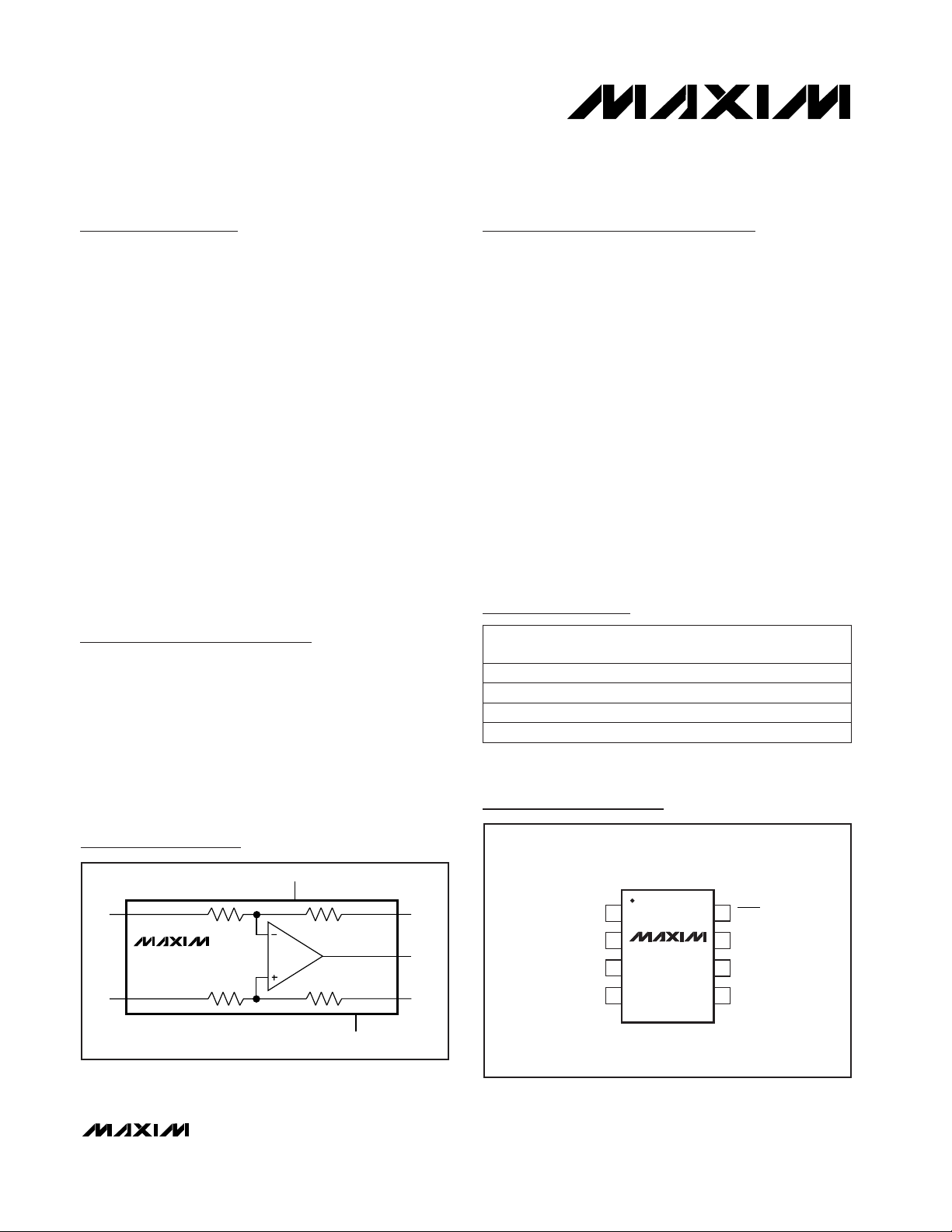
OUT
FBV
EE
1
2
87SHDN
V
CC
IN-
IN+
REF
µMAX/SO
TOP VIEW
3
4
6
5
MAX4198
MAX4199
19-1445; Rev 0; 4/99
PART
MAX4198EUA
MAX4198ESA -40°C to +85°C
-40°C to +85°C
TEMP. RANGE
PIN-
PACKAGE
8 µMAX
8 SO
Pin Configuration
Ordering Information
Rail-to-Rail is a registered trademark of Nippon Motorola, Ltd.
Beyond-the-Rails is a trademark of Maxim Integrated Products.
GAIN
(V/V)
1
1
MAX4199EUA
MAX4199ESA10-40°C to +85°C
-40°C to +85°C 8 µMAX
8 SO 10
MAX4198
MAX4199
V
CC
25k (250k)25k
25k (250k)25k
7
V
EE
( ) ARE FOR MAX4199 ONLY.
5
FB
IN-
IN+
2
3
OUT
REF
6
1
4
Functional Diagram
Page 2
MAX4198/MAX4199
Micropower, Single-Supply, Rail-to-Rail
Precision Differential Amplifiers
2 _______________________________________________________________________________________
ABSOLUTE MAXIMUM RATINGS
ELECTRICAL CHARACTERISTICS—MAX4198 (+5V Supply)
(VCC= +5V, VEE= 0V, RL= 25kΩ tied to VCC/ 2, V
REF
= VCC/ 2, V
SHDN
= VCC- 1.5V, typical values are at TA= +25°C,
T
A
= T
MIN
to T
MAX
, unless otherwise noted.) (Note 1)
Stresses beyond those listed under “Absolute Maximum Ratings” may cause permanent damage to the device. These are stress ratings only, and functional
operation of the device at these or any other conditions beyond those indicated in the operational sections of the specifications is not implied. Exposure to
absolute maximum rating conditions for extended periods may affect device reliability.
Supply Voltage (VCCto VEE)..................................................+8V
All Other Pins to GND ......................(V
EE
- 0.3V) to (VCC+ 0.3V)
Output Short Circuit Duration (to V
CC
or VEE)............Continuous
Continuous Power Dissipation (T
A
= +70°C)
SO (derate 9.09mW/°C above +70°C)..........................471mW
µMAX (derate 4.1mW/°C above +70°C) .......................330mW
Operating Temperature Range ...........................-40°C to +85°C
Junction Temperature......................................................+150°C
Storage Temperature Range............................ -65°C to +150°C
Lead Temperature (soldering, 10sec).............................+300°C
V
EE
+ 0.1V ≤
V
OUT
≤ VCC-
0.1V
Sink/source
RL= 5kΩ, ±10mV input overdrive
RL= 25kΩ, ±10mV input overdrive
f = 0.1Hz to 10Hz
f = 10kHz
VCM= VEE- 0.1V
to VCC+ 0.1V
f = 100Hz
f = 10Hz
Common-mode
IN- differential-mode
MAX4198ESA
MAX4198EUA
IN+ differential-mode
+2.7V ≤ VCC≤ +7.5V, VCM= +1.5V,
V
REF
= +1.5V, RL= 25kΩ to +1.5V
CONDITIONS
Gain Temperature Coefficient ppm/°C
±0.2 ±3
±0.01 ±0.1
mA±5.5Short-Circuit Current
V
EE
+ 0.2 V
EE
+ 0.1 to
to V
CC
- 0.2 V
CC
- 0.1
Output Voltage Swing V
V
EE
+ 0.1 V
EE
+ 0.03 to
to V
CC
- 0.1 V
CC
- 0.03
µV
RMS
7.8
Input Noise Voltage
nV√Hz
58
60
120
dB90 115PSRPower-Supply Rejection
±1.35 ±3.75
2.7 7.5
dB
74 90
CMR
DC
DC Common-Mode Rejection
kΩ
50
R
IN
25
Input Resistance
VV
CC
Supply Voltage Range
(Note 2)
±0.5 ±5
µV/°C
±1 ±20
TCOInput Offset Voltage Drift
50
UNITSMIN TYP MAXSYMBOLPARAMETER
Single supply
Dual supply
Guaranteed by CMR test VVEE- 0.1 VCC+ 0.1V
IN
Input Voltage Range
VCM= VEE- 0.1 to VCC+ 0.1V,
f = 60Hz, f = 120Hz
dB90CMR
AC
AC Common-Mode Rejection
RL= 25kΩ, VEE+ 0.1V ≤
V
OUT
≤ VCC- 0.1V
VCM= V
CC
/ 2,
TA= +25°C
RL= 5kΩ, VEE+ 0.2V ≤
V
OUT
≤ VCC- 0.2V
%
±0.01 ±0.1
Gain Error
MAX4198ESA
±0.65 ±6MAX4198EUA
VEE+ 0.1V ≤ V
OUT
≤ VCC- 0.1VNonlinearity %±0.0003
70 90MAX4198EUA
MAX4198ESA
TA= +25°C,
VCM= VCC/ 2
TA= T
MIN
to T
MAX
,
VCM= VCC/ 2
±750
±100 ±1000
±30 ±500
µV
±2300
V
OS
Input Offset Voltage
MAX4198ESA
MAX4198EUA
MAX4198ESA
MAX4198EUA
Page 3
MAX4198/MAX4199
Micropower, Single-Supply, Rail-to-Rail
Precision Differential Amplifiers
_______________________________________________________________________________________ 3
ELECTRICAL CHARACTERISTICS—MAX4198 (+5V Supply) (continued)
(VCC= +5V, VEE= 0V, RL= 25kΩ tied to VCC/ 2, V
REF
= VCC/ 2, V
SHDN
= VCC- 1.5V, typical values are at TA= +25°C,
T
A
= T
MIN
to T
MAX
, unless otherwise noted.) (Note 1)
ELECTRICAL CHARACTERISTICS—MAX4198 (+3V Supply)
(VCC= +3V, VEE= 0V, RL= 25kΩ tied to VCC/ 2, V
REF
= VCC/ 2, V
SHDN
= VCC- 1.5V, typical values are at TA= +25°C, TA= T
MIN
to T
MAX,
unless otherwise noted.) (Note 1)
V
OUT
= 3.5V, settled to within 0.1%
V
SHDN
= V
IL
V
SHDN
= VCC- 1.5V or V
SHDN
= V
EE
VCM= VCC/ 2, V
IN+
= V
IN-
V
OUT
= 2Vp-p, f = 1kHz
CONDITIONS
µs800Power-Up Delay
µA-0.1 0.1
SHDN Input Bias Current
VVCC- 2.5V
IL
Input Logic Voltage Low (Note 3)
VVCC- 1.5V
IH
Input Logic Voltage High (Note 3)
µA6.5 12I
SHDN
Shutdown Supply Current
µA45 55I
CC
Supply Current
pF690C
L
Capacitive Load Stability
%0.001THDTotal Harmonic Distortion
UNITSMIN TYP MAXSYMBOLPARAMETER
V
SHDN
= VCC- 2.5V to VCC- 1.5V,
V
OUT
= 3.5V, settled to within 0.1%
µs28t
ON/OFF
Enable/Disable Settling Time
±0.65 ±6
VEE+ 0.1V ≤
V
OUT
≤ VCC-
0.1V
MAX4198ESA
Guaranteed by CMR test
VCM= V
CC
/ 2,
TA= +25°C
Sink/source
V
RL= 5kΩ, ±10mV input overdrive
VEE- 0.1 VCC+ 0.1
RL= 25kΩ, ±10mV input overdrive
RL= 25kΩ, VEE+ 0.1V ≤
V
OUT
≤ VCC- 0.1V
VCM= VEE- 0.1
to VCC+ 0.1
TA= +25°C,
VCM= VCC/ 2
MAX4198ESA
MAX4198EUA
RL= 5kΩ, VEE+ 0.2V ≤
V
OUT
≤ VCC- 0.2V
CONDITIONS
MAX4198EUA
Gain Temperature Coefficient ppm/°C
±0.2 ±3
±0.01 ±0.1
%
±0.01 ±0.1
mA±4.5Short-Circuit Current
V
EE
+ 0.2 V
EE
+ 0.1 to
to V
CC
- 0.2 V
CC
- 0.1
Output Voltage Swing V
V
EE
+ 0.1 V
EE
+ 0.03 to
to V
CC
- 0.1 V
CC
- 0.03
Gain Error
±850
V
IN
Input Voltage Range
±100 ±1100
±35 ±600
dB
74 90
CMR
DC
DC Common-Mode Rejection
µV
±2400
V
OS
Input Offset Voltage
±0.5 ±5.0
µV/°C
±1.0 ±20
TCOInput Offset Voltage Drift
UNITSMIN TYP MAXSYMBOLPARAMETER
MAX4198ESA
MAX4198EUA
MAX4198ESA
MAX4198EUA
6.5
VCM= V
CC
/ 2, V
DIFF
= 0I
CC
Supply Current µA42
µAI
SHDN
Shutdown Supply Current
VCC- 2.5
V
IH
Input Logic High Voltage (Note 3) VVCC- 1.5
VV
IL
Input Logic Low Voltage (Note 3)
TA= T
MIN
to T
MAX
,
VCM= VCC/ 2
70 90MAX4198EUA
MAX4198ESA
V
OUT
= 2Vp-p step µs34t
s
Settling Time to 0.1%
V
OUT
= 2Vp-p step V/µs0.07SRSlew Rate
V
OUT
≤ 0.1Vp-p, VCM= VCC/ 2 kHz175BW
-3dB
-3dB Bandwidth
Page 4
MAX4199EUA
MAX4198/MAX4199
Micropower, Single-Supply, Rail-to-Rail
Precision Differential Amplifiers
4 _______________________________________________________________________________________
ELECTRICAL CHARACTERISTICS—MAX4199 (+5V Supply)
(VCC= +5V, VEE= 0V, RL= 25kΩ tied to VCC/ 2, V
REF
= VCC/ 2, V
SHDN
= VCC- 1.5V, typical values are at TA= +25°C,
T
A
= T
MIN
to T
MAX
, unless otherwise noted.) (Note 1)
±2 ±10
VEE+ 0.1V ≤
V
OUT
≤ VCC-
0.1V
MAX4199ESA
Guaranteed by CMR test
VCM= V
CC
/ 2,
TA= +25°C
Sink/source
V
RL= 5kΩ, ±10mV input overdrive
VEE- 0.1 VCC- 1.0
RL= 25kΩ, ±10mV input overdrive
f = 0.1Hz to 10Hz
f = 10kHz
RL= 25kΩ, VEE+ 0.1V ≤
V
OUT
≤ VCC- 0.1V
VCM= VEE- 0.1V
to VCC- 1.0V
f = 100Hz
f = 10Hz
Single supply
MAX4199ESA
MAX4199EUA
RL= 5kΩ, VEE+ 0.2V ≤
V
OUT
≤ VCC- 0.2V
+2.7V ≤ VCC≤ +7.5V, VCM= +1.5V,
V
REF
= +1.5V, RL= 25kΩ to +1.5V
CONDITIONS
MAX4199EUA
600
Gain Temperature Coefficient ppm/°C
±1 ±5
0.1
VEE+ 0.1V ≤ V
OUT
≤ VCC- 0.1VNonlinearity %±0.0003
±0.01 ±0.3
%
±0.01 ±0.3
mA±5.5Short-Circuit Current
V
OUT
= 2Vp-p
V
EE
+ 0.2 V
EE
+ 0.1 to
to V
CC
- 0.2 V
CC
- 0.1
Output Voltage Swing V
V
EE
+ 0.1 V
EE
+ 0.02 to
to V
CC
- 0.1 V
CC
- 0.02
Gain Error
µV
RMS
6.6
Input Noise Voltage
nV√Hz
38
C
L
Capacitive Load Stability pF
40
45V
OUT
≤ 0.1Vp-p, VCM= VCC/ 2
SR
60
BW
-3dB
-3dB Bandwidth kHz
Slew Rate V/µs
dB90 120PSRPower-Supply Rejection
V
IN
Input Voltage Range (Note 2)
±1.35 ±3.75
VCM= VEE- 0.1V to VCC- 1.0V, f = 60Hz
2.7 7.5
dB110CMR
AC
dB
84 110
CMR
DC
DC Common-Mode Rejection
kΩ
275
R
IN
AC Common-Mode Rejection
25Input Resistance
VV
CC
Supply Voltage Range (Note 2)
±0.25 ±3
µV/°C
±0.75 ±15
TCOInput Offset Voltage Drift
275
UNITSMIN TYP MAXSYMBOLPARAMETER
IN+ differential mode
IN- differential mode
Common-mode
37V
OUT
= 2Vp-p stept
s
Settling Time to 0.1% µs
0.001V
OUT
= 2Vp-p, f = 1kHzTHDTotal Harmonic Distortion %
6.5 12V
SHDN
= V
IL
45 55VCM= VCC/ 2, V
IN+
= V
IN-
I
CC
Supply Current µA
I
SHDN
Shutdown Supply Current µA
80 110MAX4199EUA
MAX4199ESA
TA= +25°C,
VCM= VCC/ 2
TA= T
MIN
to T
MAX
,
VCM= VCC/ 2
±500
±100 ±600
±10 ±300
µV
±1475
V
OS
Input Offset Voltage
MAX4199ESA
MAX4199EUA
MAX4199ESA
MAX4199EUA
Dual supply
Page 5

MAX4198/MAX4199
Micropower, Single-Supply, Rail-to-Rail
Precision Differential Amplifiers
_______________________________________________________________________________________ 5
Note 1: The MAX4198EUA and the MAX4199EUA are 100% production tested at +25°C. All temperature limits are guaranteed
by design.
Note 2: Guaranteed by PSR test.
Note 3: When shutdown input is at logic high, the part is active; when at logic low, the part is in shutdown.
ELECTRICAL CHARACTERISTICS—MAX4199 (+5V Supply) (continued)
(VCC= +5V, VEE= 0V, RL= 25kΩ tied to VCC/ 2, V
REF
= VCC/ 2, V
SHDN
= VCC- 1.5V, typical values are at TA= +25°C,
T
A
= T
MIN
to T
MAX
, unless otherwise noted.) (Note 1)
V
SHDN
= VCC- 2.5V to VCC- 1.5V,
V
OUT
= 3.5V, settled to within 0.1%
µs35t
ON/OFF
Enable/Disable Settling Time
V
OUT
= 3.5V, settled to within 0.1%
V
SHDN
= VCC- 1.5V or V
SHDN
= V
EE
CONDITIONS
µs800Power-Up Delay
µA-0.1 0.1
SHDN Input Bias Current
VVCC- 2.5V
IL
Input Logic Voltage Low
(Note 3)
VVCC- 1.5V
IH
Input Logic Voltage High
(Note 3)
UNITSMIN TYP MAXSYMBOLPARAMETER
ELECTRICAL CHARACTERISTICS—MAX4199 (+3V Supply)
(VCC= +3V, VEE= 0V, RL= 25kΩ tied to VCC/ 2, V
REF
= VCC/ 2, V
SHDN
= VCC- 1.5V, values are at TA= +25°C,
T
A
= T
MIN
to T
MAX
, unless otherwise noted.) (Note 1)
±2 ±10
VEE+ 0.1V ≤
V
OUT
≤ VCC-
0.1V
MAX4199ESA
Guaranteed by CMR test
VCM= V
CC
/ 2,
TA= +25°C
Sink/source
V
RL= 5kΩ, ±10mV input overdrive
VEE- 0.1 VCC- 1.1
RL= 25kΩ, ±10mV input overdrive
6.5
RL= 25kΩ, VEE+ 0.1V ≤
V
OUT
≤ VCC- 0.1V
VCM= VEE- 0.1
to VCC- 1.1
VCM= V
CC
/ 2, V
DIFF
= 0I
CC
Supply Current
TA= +25°C,
VCM= VCC/ 2
MAX4199ESA
MAX4199EUA
RL= 5kΩ, VEE+ 0.2V ≤
V
OUT
≤ VCC- 0.2V
µA42
CONDITIONS
MAX4199EUA
µA
Gain Temperature Coefficient ppm/°C
±1 ±5
I
SHDN
Shutdown Supply Current
VCC- 2.5
±0.01 ±0.3
%
±0.01 ±0.3
mA±4.5Short-Circuit Current
V
IH
V
EE
+ 0.2 V
EE
+ 0.1 to
to V
CC
- 0.2 V
CC
- 0.1
Output Voltage Swing V
V
EE
+ 0.1 V
EE
+ 0.02 to
to V
CC
- 0.1 V
CC
- 0.02
Gain Error
Input Logic High Voltage (Note 3) VVCC- 1.5
VV
IL
Input Logic Low Voltage (Note 3)
±600
V
IN
Input Voltage Range
±100 ±700
±15 ±400
dB
84 110
CMR
DC
DC Common-Mode Rejection
µV
±1675
V
OS
Input Offset Voltage
±0.25 ±5
µV/°C
±0.75 ±15
TCOInput Offset Voltage Drift
UNITSMIN TYP MAXSYMBOLPARAMETER
MAX4199ESA
MAX4199EUA
MAX4199ESA
MAX4199EUA
TA= T
MIN
to T
MAX
,
VCM= VCC/ 2
80 110MAX4199EUA
MAX4199ESA
Page 6

MAX4198/MAX4199
Micropower, Single-Supply, Rail-to-Rail
Precision Differential Amplifiers
6 _______________________________________________________________________________________
Typical Operating Characteristics
(VCC= +5V, VEE= 0V, RL= 25kΩ to VCC/ 2, V
SHDN
= VCC- 1.5V, small-signal V
OUT
= 100mVp-p, large-signal V
OUT
= 1Vp-p,
TA= +25°C, unless otherwise noted.)
35
37
36
39
38
41
40
42
44
43
45
SUPPLY CURRENT vs. TEMPERATURE
MAX4198toc01
TEMPERATURE (°C)
SUPPLY CURRENT (µA)
-40 10-15 35 60 85
MAX4198
MAX4199
100k 1M
0.1k
3
2
1
0
-1
-2
-3
-4
-5
-6
1k 10k
FREQUENCY (Hz)
MAX4198
SMALL-SIGNAL GAIN vs. FREQUENCY
MAX4198toc02
GAIN (dB)
100k 1M
0.1k 1k 10k
MAX4199
SMALL-SIGNAL GAIN vs. FREQUENCY
MAX4198toc03
FREQUENCY (Hz)
3
2
1
0
-1
-2
-3
-4
-5
-6
NORMALIZED GAIN (dB)
-10
-130
-110
1 10 100 1k 10k 100k
POWER-SUPPLY REJECTION vs.
FREQUENCY
-90
MAX4198toc04
FREQUENCY (Hz)
PSR (dB)
-70
-50
-30
MAX4199
MAX4198
-120
-110
-100
-90
-80
-70
-60
COMMON-MODE REJECTION vs.
TEMPERATURE
MAX4198toc07
TEMPERATURE (°C)
CMR (dB)
-40 10-15 35 60 85
MAX4198
MAX4199
0
-120
-100
10 100 1k 10k 100k 1M
COMMON-MODE REJECTION vs.
FREQUENCY
-80
MAX4198toc05
FREQUENCY (Hz)
CMR (dB)
-60
-40
-20
MAX4199
MAX4198
800
-1000
0.1 100101
OUTPUT VOLTAGE HIGH AND LOW vs.
LOAD RESISTANCE
-400
-800
400
0
1000
-200
-600
600
200
MAX4198toc06
LOAD (kΩ)
VOLTAGE (mV)
MAX4199
V
OH
- V
CC
V
OL
- V
EE
MAX4198
MAX4199
MAX4198
-40 10-15 35 60 85
-100
-50
0
50
100
INPUT OFFSET VOLTAGE
vs. TEMPERATURE
MAX4198toc08
TEMPERATURE (°C)
INPUT OFFSET VOLTAGE (µV)
MAX4199
MAX4198
-40 10-15 35 60 85
-0.014
-0.008
-0.010
-0.012
-0.006
0
-0.004
-0.002
0.004
0.002
0.008
0.006
GAIN ERROR vs. TEMPERATURE
MAX4198toc09
TEMPERATURE (°C)
GAIN ERROR (%)
MAX4199
MAX4198
Page 7

MAX4198/MAX4199
Micropower, Single-Supply, Rail-to-Rail
Precision Differential Amplifiers
_______________________________________________________________________________________
7
10k
10
1 1k 10k10010 100k
VOLTAGE NOISE DENSITY
vs. FREQUENCY
100
1k
MAX4198toc10
FREQUENCY (Hz)
VOLTAGE NOISE DENSITY (nV/
√
Hz)
MAX4198
MAX4199
1.000
0
100 1k 10k
TOTAL HARMONIC DISTORTION
VOLTAGE NOISE vs. FREQUENCY
0.010
0.001
0.100
MAX4198toc11
FREQUENCY (Hz)
THD + VOLTAGE NOISE (%)
MAX4199
MAX4198
50µs/div
SMALL-SIGNAL PULSE RESPONSE
INPUT
50mV/div
OUTPUT
50mV/div
MAX4198toc12
50µs/div
MAX4199
SMALL-SIGNAL PULSE RESPONSE
INPUT
5mV/div
OUTPUT
50mV/div
MAX4198toc13
50µs/div
MAX4198
LARGE-SIGNAL PULSE RESPONSE
INPUT
500mV/div
OUTPUT
500mV/div
MAX4198toc14
50µs/div
MAX4199
LARGE-SIGNAL PULSE RESPONSE
INPUT
50mV/div
OUTPUT
500mV/div
MAX4198toc15
Typical Operating Characteristics (continued)
(VCC= +5V, VEE= 0V, RL= 25kΩ to VCC/ 2, V
SHDN
= VCC- 1.5V, small-signal V
OUT
= 100mVp-p, large-signal V
OUT
= 1Vp-p,
TA= +25°C, unless otherwise noted.)
50µs/div
MAX4198
SMALL-SIGNAL PULSE RESPONSE
WITH CAPACITIVE LOAD
INPUT
50mV/div
OUTPUT
50mV/div
MAX4198toc16
CL = 690pF
50µs/div
MAX4198
SMALL-SIGNAL PULSE RESPONSE
WITH EXCESSIVE CAPACITIVE LOAD
INPUT
50mV/div
OUTPUT
50mV/div
MAX4198toc17
CL = 1060pF
R
ISO
= 0Ω
50µs/div
MAX4198
SMALL-SIGNAL PULSE RESPONSE WITH
EXCESSIVE CAPACITIVE LOAD
AND ISOLATION RESISTOR
INPUT
50mV/div
OUTPUT
50mV/div
MAX4198toc18
CL = 1060pF
R
ISO
= 50Ω
Page 8

MAX4198/MAX4199
Micropower, Single-Supply, Rail-to-Rail
Precision Differential Amplifiers
8 _______________________________________________________________________________________
Typical Operating Characteristics (continued)
(VCC= +5V, VEE= 0V, RL= 25kΩ to VCC/ 2, V
SHDN
= VCC- 1.5V, small-signal V
OUT
= 100mVp-p, large-signal V
OUT
= 1Vp-p,
TA= +25°C, unless otherwise noted.)
50µs/div
MAX4199
SMALL-SIGNAL PULSE RESPONSE
WITH CAPACITIVE LOAD
INPUT
5mV/div
OUTPUT
50mV/div
MAX4198toc19
CL = 590pF
50µs/div
MAX4199
SMALL-SIGNAL PULSE RESPONSE WITH
EXCESSIVE CAPACITIVE LOAD
INPUT
5mV/div
OUTPUT
50mV/div
MAX4198toc20
CL = 760pF
R
ISO
= 0Ω
50µs/div
MAX4199
SMALL-SIGNAL PULSE RESPONSE WITH
EXCESSIVE CAPACITIVE LOAD
AND ISOLATION RESISTOR
INPUT
5mV/div
OUTPUT
50mV/div
MAX4198toc21
CL = 760pF
R
ISO
= 75Ω
0
60
40
20
80
120
100
-300-240 -120-180 -60 0 12060 180 240 300
MAX4199 HISTOGRAM
(V
OS
BASED ON 280 UNITS)
MAX4198toc25
VOS (µV)
COUNT
0
30
40
20
10
70
60
50
100
90
80
-0.08 -0.06 -0.04 -0.02 0 0.02 0.04 0.06 0.08
MAX4198 HISTOGRAM
(GAIN ACCURACY BASED ON 200 UNITS)
MAX4198toc26
GAIN ERROR (%)
COUNT
0
40
20
100
80
60
160
140
120
-0.24 -0.18 -0.12 -0.06 0 -0.06 0.12 0.18 0.24
MAX4199 HISTOGRAM
(GAIN ACCURACY BASED ON 280 UNITS)
MAX4198toc27
GAIN ERROR (%)
COUNT
10µs/div
MAX4198
TIME EXITING SHUTDOWN
INPUT
(SHDN PIN)
500mV/div
OUTPUT
500mV/div
MAX4198toc22
10µs/div
MAX4199
TIME EXITING SHUTDOWN
INPUT
(SHDN PIN)
500mV/div
OUTPUT
500mV/div
MAX4198toc23
0
30
20
10
40
60
50
-300-240 -120-180 -60 0 12060 180 240 300
MAX4198 HISTOGRAM
(V
OS
BASED ON 200 UNITS)
MAX4198toc24
V
(µV)
COUNT
Page 9

_______________Detailed Description
The MAX4198/MAX4199 are precision low-power differential amplifiers with factory-trimmed internal gain-setting resistors. The MAX4198 is trimmed to a gain of
+1V/V and the MAX4199 is trimmed to a gain of +10V/V.
Input Stage
The
Functional Diagram
shows the internal structure of
the MAX4198/MAX4199. Although the resistors are precision matched, their absolute value varies by ±25%.
The typical input impedance for the MAX4198 is 50kΩ
for the noninverting input and 25kΩ for the inverting
input. The typical input impedance for the MAX4199 is
275kΩ for the noninverting input and 25k Ω for the
inverting input.
The common-mode inputs of the internal op amp can
range from V
EE
to (VCC- 1.1V). Although the inputs to
the internal op amp are not rail-to-rail, the internal resistors form a voltage divider that extends the input common-mode range beyond-the-rails for the MAX4198.
The overall input range of the MAX4198 extends 100mV
beyond-the-rails without adversely affecting commonmode rejection or undergoing phase reversal (VCC=
5V). The MAX4199 input common-mode range extends
from 100mV below the negative rail to (VCC- 1V) (see
the Input Common-Mode Voltage Range vs. Supply
Voltage graph in the
Typical Operating Characteristics
).
MAX4198/MAX4199
Micropower, Single-Supply, Rail-to-Rail
Precision Differential Amplifiers
_______________________________________________________________________________________ 9
-0.5
1.5
0.5
4.5
3.5
2.5
7.5
6.5
5.5
243 5678
MAX4199
INPUT COMMON-MODE RANGE vs.
SUPPLY VOLTAGE
MAX4198toc28
SUPPLY VOLTAGE (V)
INPUT COMMON-MODE VOLTAGE (V)
V
REF
= VCC/2
Typical Operating Characteristics (continued)
(VCC= +5V, VEE= 0V, RL= 25kΩ to VCC/ 2, V
SHDN
= VCC- 1.5V, small-signal V
OUT
= 100mVp-p, large-signal V
OUT
= 1Vp-p,
TA= +25°C, unless otherwise noted.)
-0.5
1.5
0.5
4.5
3.5
2.5
7.5
6.5
5.5
8.5
243 5678
MAX4198
INPUT COMMON-MODE RANGE vs.
SUPPLY VOLTAGE
MAX4198toc29
SUPPLY VOLTAGE (V)
INPUT COMMON-MODE VOLTAGE (V)
V
REF
= VCC/2
Pin Description
Feedback Resistor. Can be used as a sense input.FB5
Amplifier OutputOUT6
Positive Supply VoltageV
CC
7
Shutdown Control. Shutdown threshold is referenced to VCC. When pulled 2.5V below VCC, part
is in shutdown.
SHDN
8
Negative Supply VoltageV
EE
4
Noninverting InputIN+3
PIN
Inverting InputIN-2
Reference Voltage Input. Offsets output voltage.REF1
FUNCTIONNAME
Page 10

MAX4198/MAX4199
Rail-to-Rail Output Stage
The MAX4198/MAX4199 output stage incorporates a
common-source rail-to-rail structure which maximizes the
dynamic range of the differential amplifier. The output
can swing to within 100mV from each rail with a 5kΩ load
to VCC/ 2 (see
Typical Operating Characteristics
).
Shutdown Mode
The MAX4198/MAX4199 have an active-low shutdown
input. SHDN input logic thresholds are referenced to
VCC, not to GND. Pulling SHDN 2.5V below the positive
rail places the amplifiers in a 12µA (max) shutdown
mode. The MAX4198/MAX4199 exit or enter shutdown
in 35µs. In shutdown, the OUT pin is high-impedance.
Applications Information
Driving Capacitive Loads
The MAX4198/MAX4199 are relatively immune to oscillations caused when driving large capacitive loads.
Although heavy load capacitance increases transient ringing, sustained oscillations typically don’t occur for loads
under 600pF (see Pulse Response with Capacitive Load
in the
Typical Operating Characteristics
). Applications that
require driving higher capacitive loads can isolate the output capacitance using a 15Ω to 100Ω resistor between the
amplifier output and the load (Figure 1). Although adding
an isolation resistor dampens the response enough to prevent oscillations, it does so at the expense of bandwidth
and DC accuracy.
Power Supply Considerations
The MAX4198/MAX4199 operate from single +2.7V to
+7.5V supplies or from dual ±1.35V to ±3.75V supplies,
and they consume only 45µA of supply current.
Excellent power-supply rejection permits the amplifiers
to be operated directly from a decaying 3V cell without
excessive error. To maximize AC performance, the supply must be bypassed with a 0.1µF ceramic capacitor
to ground that must be as close as possible to the pin.
If dual supplies are used, bypass both supply pins with
0.1µF to ground.
Application Circuits
Differential amplifiers can be used in single-ended and
other amplifier applications. Figures 2 through 6 show
the MAX4198/MAX4199 in different configurations. The
internally trimmed and matched resistors offer convenience and have a distinct advantage over external
resistors. These amplifiers are not compensated for single-ended unity gain; therefore, IN- should not be connected to OUT or left unconnected.
Micropower, Single-Supply, Rail-to-Rail
Precision Differential Amplifiers
10 ______________________________________________________________________________________
MAX4198
MAX4199
R
ISO
FB
OUT
V
EE
V
CC
INPUT
IN+
IN-
REF
C
L
R
L
OUTPUT
Figure 1. Dual-Supply, Capacitive-Load Driving Circuit
MAX4198
MAX4199
FB
OUT
V
EE
V
CC
IN+
IN-
V
A
V
B
REF
V
OUT
V
OUT
= (VB - VA)
(MAX4198)
V
OUT
= 10 (VB - VA)
(MAX4199)
Figure 2. Standard Difference Amplifier
MAX4198
MAX4199
FB
OUT
V
EE
V
CC
IN+
IN-
V
A
REF
V
OUT
V
OUT
= -VA (MAX4198)
V
OUT
= -10VA (MAX4199)
Figure 3. Precision Inverting Buffer
Page 11

Instrumentation Amplifier Applications
For applications that require a complete low-power
instrumentation amplifier, refer to the MAX4194–
MAX4197 data sheet. Some differential to single-ended
voltage amplifier applications that don’t require a high
input impedance can use the MAX4198/MAX4199 for
gains of +1V/V or +10V/V. The MAX4198/MAX4199 can
also be used as an instrumentation amplifier building
block. The circuit of Figure 7 takes advantage of the
10pA (max), 0.1pA (typ) bias current of the MAX406A
to form an instrumentation amplifier similar to the
MAX4194 family, except with lower input bias currents.
The MAX406A's low 1.2µA supply current maintains a
low overall supply current.
MAX4198/MAX4199
Micropower, Single-Supply, Rail-to-Rail
Precision Differential Amplifiers
______________________________________________________________________________________ 11
MAX4198
5
FB
6
OUT
V
EE
V
CC
1
3
IN+
V
A
REF
2
IN-
V
OUT
V
OUT
= 2V
A
Figure 4. Precision Gain of Two Amplifiers
MAX4198
FB
IN+
V
CC
OUT
IN-
V
A
V
CC
REF
V
OUT
V
OUT
= -V
A
Figure 5. Single-Supply Inverting Amplifier Biased at VCC/ 2
MAX4198
5
2
IN-
3
IN+
5
COM
1
REF
1
4
NC
6
NO
IN
FB
6
OUT
V
EE
LOGIC
IN
V
OUT
0
1
-V
A
+V
A
NOTE: MAX4544 PINOUT FOR 6-PIN SOT23-6
V
CC
V
A
V
OUT
MAX4544
Figure 6. Digitally Controlled Precision Gain of ±1 Amplifier
MAX4198
FB
IN-
V
A
IN+
OUT
REF
A1, A2 = MAX406A
V
OUT
= (1 + 2R2 / R1) (VB - VA)
V
OUT
V
B
A2
A1
R
2
R
1
R
2
Figure 7. Ultra-Low Input Bias Current (0.1pA) Instrumentation
Amplifiers with 47µA Supply-Current Consumption
Page 12

MAX4198/MAX4199
Micropower, Single-Supply, Rail-to-Rail
Precision Differential Amplifiers
Maxim cannot assume responsibility for use of any circuitry other than circuitry entirely embodied in a Maxim product. No circuit patent licenses are
implied. Maxim reserves the right to change the circuitry and specifications without notice at any time.
12
____________________Maxim Integrated Products, 120 San Gabriel Drive, Sunnyvale, CA 94086 408-737-7600
© 1999 Maxim Integrated Products Printed USA is a registered trademark of Maxim Integrated Products.
Package Information
Chip Information
TRANSISTOR COUNT: 250
SUBSTRATE CONNECTED TO V
EE
8LUMAXD.EPS
 Loading...