

Page 1
General Description
The MAX4162/MAX4163/MAX4164 are single/dual/quad,
micropower operational amplifiers that combine an
exceptional bandwidth to power consumption ratio with
true rail-to-rail inputs and outputs. They consume a
mere 25µA quiescent current per amplifier, yet achieve
200kHz gain-bandwidth product and are unity-gain
stable while driving any capacitive load. The MAX4162/
MAX4163/MAX4164 operate from either a single supply
(2.7V to 10V) or dual supplies (±1.35V to ±5V), with an
input common-mode voltage range that extends 250mV
beyond either supply rail. These amplifiers use a proprietary architecture to achieve a very high input commonmode rejection ratio without the midswing nonlinearities
present in other Rail-to-Rail®op amps. This architecture also maintains high open-loop gain and output
swing while driving substantial loads.
The combination of excellent bandwidth/power performance, single-supply operation, and miniature footprint
makes these op amps ideal for portable equipment and
other low-power, single-supply applications. The single
MAX4162 is available in 8-pin SO and space-saving
5-pin SOT23 packages. The MAX4163 is available in an 8pin ultra chip-scale package (UCSP™) and an 8-pin µMAX
or SO package. The MAX4164 is available in a 14-pin SO
package.
________________________Applications
Battery-Powered Devices Medical Instruments
pH Probes Ionization Detectors
Portable Equipment Cellular Phones
Low-Power, Low-Voltage
Equipment
Features
♦ UCSP Package (MAX4163)
♦ 1.0pA Typical Input Bias Current
♦ Single-Supply Operation from 2.7V to 10V
♦ Input Common-Mode Voltage Range Extends
250mV Beyond Either Supply Rail
♦ Rail-to-Rail Output Swing
♦ 200kHz Gain-Bandwidth Product
♦ 25µA Quiescent Current per Amplifier
♦ Excellent CMRR, PSRR, and Gain Linearity
♦ No Phase Reversal for Overdriven Inputs
♦ Unity-Gain Stable
♦ Stable with Any Capacitive Load
♦ Internally Short-Circuit Protected to Either Rail
MAX4162/MAX4163/MAX4164
UCSP, Micropower, Single-Supply, 10V,
Rail-to-Rail I/O Op Amps
________________________________________________________________ Maxim Integrated Products 1
Typical Application Circuit
Pin Configurations
19-1195; Rev 1; 3/02
PART
MAX4162ESA
-40°C to +85°C
TEMP
RANGE
PINPACKAGE
8 SO
Ordering Information
For pricing, delivery, and ordering information, please contact Maxim/Dallas Direct! at
1-888-629-4642, or visit Maxim’s website at www.maxim-ic.com.
TOP
MARK
—
TOP VIEW TOP VIEW (BUMPS SIDE DOWN)
V
SS
IN-
IN+
1
5
V
DD
OUT
MAX4162
MAX4163
SOT23
2
3
4
A
B
C
12 3
OUTA
V
DD
OUTB
INA-
INB-
INB+V
SS
INA+
UCSP (B9-2)
MAX4162EUK-T -40°C to +85°C 5 SOT23-5 AABX
MAX4163EBL-T*
-40°C to +85°C 8 UCSP-8 AAX
MAX4163EUA -40°C to +85°C 8 µMAX —
Pin Configurations continued at end of data sheet.
*UCSP reliability is integrally linked to the user’s assembly
methods, circuit board material, and environment. Refer to the
UCSP Reliability Notice in the UCSP Reliability section of this
data sheet for more information.
MAX4164ESD
-40°C to +85°C 14 SO —
Rail-to-Rail is a registered trademark of Nippon Motorola Ltd.
UCSP is a trademark of Maxim Integrated Products, Inc.
MAX4163ESA -40°C to +85°C 8 SO —
IN+
V
IN
MAX6120
GND
1/2 MAX4163
V
OUT
IN-
R
IN-
1/2 MAX4163
IN+
MICROPOWER ±1.2V REFERENCE
R
3V
V
DD
V
SS
V
DD
V
SS
-3V
V
OUT
+1.2V
V
V
-1.2V
V
OUT
MAX152
REF+
REF-
V
DD
V
SS
Page 2
MAX4162/MAX4163/MAX4164
UCSP, Micropower, Single-Supply, 10V,
Rail-to-Rail I/O Op Amps
2 _______________________________________________________________________________________
ABSOLUTE MAXIMUM RATINGS
ELECTRICAL CHARACTERISTICS: 3V Operation
(VDD= 3V, VSS= 0, VCM= VDD/2, V
OUT
= VDD/2, RLtied to VDD/2, TA= -40°C to +85°C, unless otherwise noted. Typical values are
at T
A
= +25°C.) (Note 1)
Stresses beyond those listed under “Absolute Maximum Ratings” may cause permanent damage to the device. These are stress ratings only, and functional
operation of the device at these or any other conditions beyond those indicated in the operational sections of the specifications is not implied. Exposure to
absolute maximum rating conditions for extended periods may affect device reliability.
Supply Voltage (VDDto VSS)..................................................11V
IN+, IN-, OUT Voltage ......................(V
DD
+ 0.3V) to (V
SS
- 0.3V)
Short-Circuit Duration (to either rail)...........................Continuous
Continuous Power Dissipation (T
A
= +70°C)
5-Pin SOT23 (derate 7.1mW/°C above +70°C)..............571mW
8-Pin SO (derate 5.88mW/°C above +70°C)..................471mW
8-Pin UCSP (derate 4.7mW/°C above +70°C) ...............379mW
8-Pin µMAX (derate 4.1mW/°C above +70°C) ...............330mW
14-Pin SO (derate 8.00mW/°C above +70°C)................640mW
Operating Temperature Range ...........................-40°C to +85°C
Storage Temperature Range .............................-65°C to +150°C
Junction Temperature......................................................+150°C
Lead Temperature (soldering, 10s) .................................+300°C
To either supply rail
VOL- V
SS
VDD- V
OH
VOL- V
SS
VDD- V
OH
Inferred from PSRR test
RL= 10kΩ
Inferred from CMRR test
TA= +25°C
TA= -40°C to +85°C
TA= +25°C
TA= -40°C to +85°C
CONDITIONS
15I
SC
mV
325
RL= 100kΩ
V
OUT
325
30 180
RL= 10kΩ
30 180
dBA
V
85 120
dBCMRR 70 100
pA1.0 100
V2.7 10.0V
DD
I
B
TΩ
VSS- VDD+
0.25 0.25
V
CM
>10R
IN
±6
±0.5 ±5
MAX4164
±0.5 ±3
V
OS
±4
MAX4162
±0.5 ±4
mV
±5
MAX4163
UNITSMIN TYP MAXSYMBOL
AV= 1V/V
kHz200GBWP
VDD= 2.7V to 10VPSRR dB80 110
mA
0.1R
OUT
V
VCM= (VSS- 0.25V) to (VDD+ 0.25V)
Ω
µV/°CTCV
OS
2
TA= +25°C
TA= -40°C to +85°C
µA25 40I
DD
degrees60
φM
dB12GM
V
OUT
= 1V to 2V step µs50
VDD= 0 to 3V step, VIN= VDD/2, AV= 1V/V µs20t
ON
V/ms115SR
f = 1kHz, V
OUT
= 2V
P-P
, RL= 100kΩ, AV= 1V/VTHD %0.02
Phase Margin
Gain Margin
Output Short-Circuit Current
Output Voltage Swing
Input Offset Voltage Tempco
Settling Time to 0.1%
Large-Signal Voltage Gain
Supply Current (Per Amplifier)
Turn-On Time
Slew Rate
Total Harmonic Distortion
Common-Mode Rejection Ratio
Operating Voltage Range
Input Bias Current (Note 2)
Input Common-Mode Voltage
Range
Differential Input Resistance
Input Offset Voltage
PARAMETER
Gain-Bandwidth Product
Power-Supply Rejection Ratio
Closed-Loop Output Resistance
Page 3
MAX4162/MAX4163/MAX4164
UCSP, Micropower, Single-Supply, 10V,
Rail-to-Rail I/O Op Amps
_______________________________________________________________________________________ 3
ELECTRICAL CHARACTERISTICS: 3V Operation (continued)
(VDD= 3V, VSS= 0, VCM= VDD/2, V
OUT
= VDD/2, RLtied to VDD/2, TA= -40°C to +85°C, unless otherwise noted. Typical values are
at T
A
= +25°C.) (Note 1)
ELECTRICAL CHARACTERISTICS: 5V Operation
(VDD= 5V, VSS= 0, VCM= VDD/2, V
OUT
= VDD/2, RLtied to VDD/2, TA= -40°C to +85°C, unless otherwise noted. Typical
values are at T
A
= +25°C.) (Note 1)
pF
CONDITIONS
nV/√Hz
e
n
80f = 1kHzInput Voltage-Noise Density
Input Common-Mode
Capacitance
pF
1.5
Differential Input Capacitance 0.7
PARAMETER UNITSMIN TYP MAXSYMBOL
kHz
Internal Charge-Pump
Frequency
700
µV
P-P
Charge-Pump Output
Feedthrough
100
To either supply rail
VOL- V
SS
VDD- V
OH
V
VOL- V
SS
VDD- V
OH
VCM= (VSS- 0.25V) to (VDD+ 0.25V)
Inferred from PSRR test
degrees60
RL= 10kΩ
Inferred from CMRR test
φM
Ω
dB
TA= +25°C
TA= -40°C to +85°C
TA= +25°C
12
TA= -40°C to +85°C
GM
CONDITIONS
15I
SC
mV
540
RL= 100kΩ
V
OUT
µV/°C
540
µA
50 300
RL= 10kΩ
2
50 300
TA= +25°C
TA= -40°C to +85°C
dBA
V
25 45I
DD
85 120
dBCMRR
Phase Margin
Gain Margin
Output Short-Circuit Current
Output Voltage Swing
70 100
Input Offset Voltage Tempco
Large-Signal Voltage Gain
Supply Current (Per Amplifier)
Common-Mode Rejection Ratio
Operating Voltage Range
pA1.0 100Input Bias Current (Note 2)
V2.7 10.0
Input Common-Mode Voltage
Range
V
DD
I
B
TΩ
VSS- VDD+
0.25 0.25
Differential Input Resistance
V
CM
Input Offset Voltage
>10
PARAMETER
Gain-Bandwidth Product
±6
Power-Supply Rejection Ratio
Closed-Loop Output Resistance
±0.5 ±5
MAX4164
±0.5 ±3
V
OS
±4
MAX4162
±0.5 ±4
mV
±5
MAX4163
UNITSMIN TYP MAXSYMBOL
AV= 1V/V
kHz200GBWP
VDD= 2.7V to 10VPSRR dB80 110
mA
0.1R
OUT
Page 4
MAX4162/MAX4163/MAX4164
UCSP, Micropower, Single-Supply, 10V,
Rail-to-Rail I/O Op Amps
4 _______________________________________________________________________________________
ELECTRICAL CHARACTERISTICS: 5V Operation (continued)
(VDD= 5V, VSS= 0, VCM= VDD/2, V
OUT
= VDD/2, RLtied to VDD/2, TA= -40°C to +85°C, unless otherwise noted. Typical
values are at T
A
= +25°C.) (Note 1)
__________________________________________Typical Operating Characteristics
(VDD= 5V, VSS= 0, VCM= VDD/2, TA = +25°C, unless otherwise noted.)
Note 1: All device specifications are 100% tested at T
A
= +25°C. Limits over the extended temperature range are guaranteed by
design, not production tested.
Note 2: Input bias current guaranteed by design, not production tested.
pF
CONDITIONS
%THD 0.02f = 1kHz, V
OUT
= 2V
P-P
, RL= 100kΩ, AV= 1V/VTotal Harmonic Distortion
Input Common-Mode
Capacitance
V/ms
1.5
Slew Rate 115
PARAMETER
SR
kHz
Internal Charge-Pump
Frequency
700
µV
P-P
Charge-Pump Output
Feedthrough
100
UNITSMIN TYP MAXSYMBOL
V
OUT
= 1V to 2V step µsSettling Time to 0.1% 70
VDD= 0 to 3V step, VIN= VDD/2, AV= 1V/V µsTurn-On Time 40t
ON
f = 1kHz
nV/√Hz
Input Voltage-Noise Density 80e
n
pFDifferential Input Capacitance 0.7
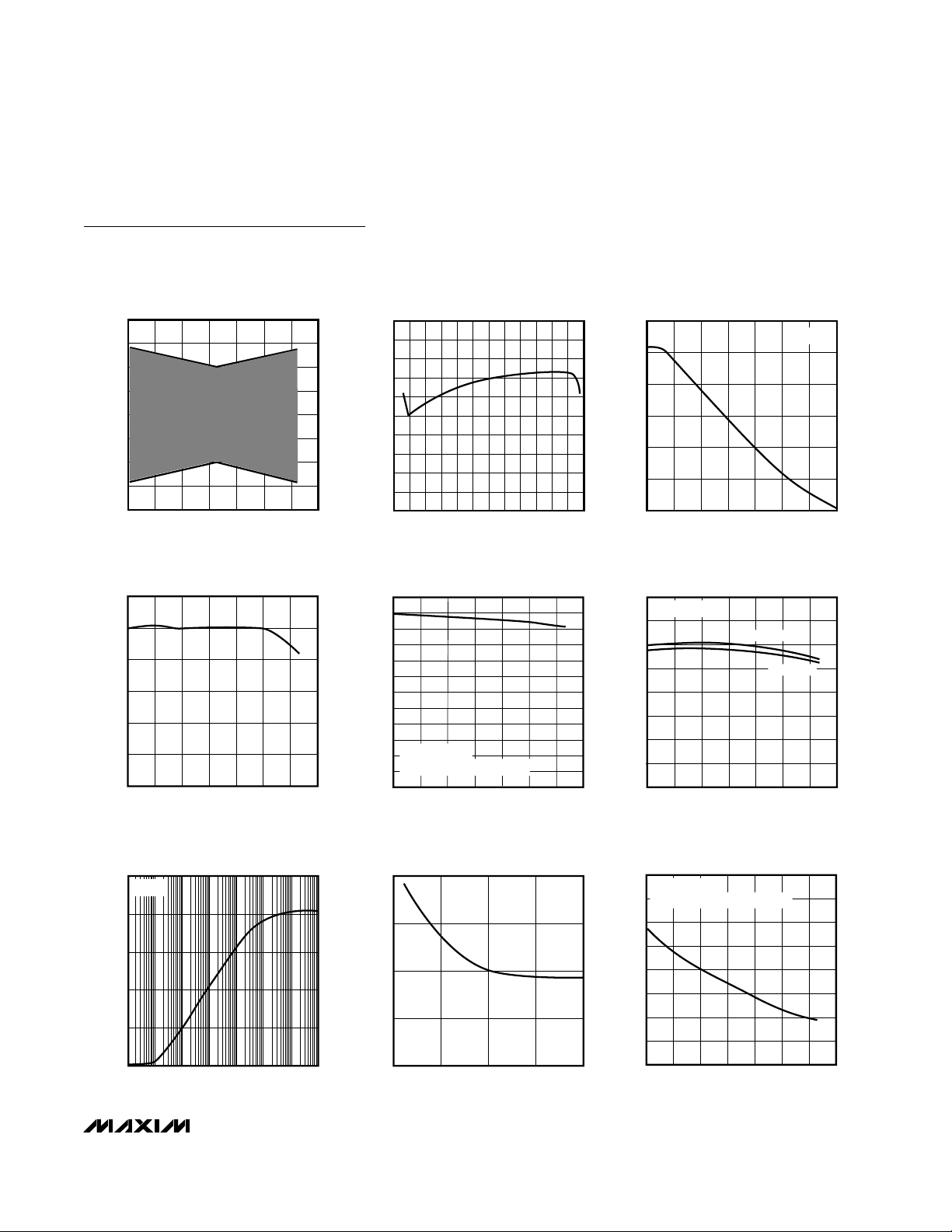
SUPPLY CURRENT
vs. SUPPLY VOLTAGE
30
25
20
15
10
SUPPLY CURRENT (µA)
5
0
123456789
SUPPLY VOLTAGE (V)
10
MAX4162-01
28
26
24
22
20
18
16
SUPPLY CURRENT (µA)
14
12
10
-40 -20 0 20
SUPPLY CURRENT
vs. TEMPERATURE
VCC = 3V
40
TEMPERATURE (°C)
MAX4162-02
VCC = 5V
60 80 100
INPUT OFFSET VOLTAGE VARIATION
vs. SUPPLY VOLTAGE
50
30
10
-10
-30
(µV)
-50
OS
V
-70
-90
-110
-130
-150
12345678910
SUPPLY VOLTAGE (V)
MAX4162-03
Page 5
MAX4162/MAX4163/MAX4164
UCSP, Micropower, Single-Supply, 10V,
Rail-to-Rail I/O Op Amps
_______________________________________________________________________________________ 5
Typical Operating Characteristics (continued)
(VDD= 5V, VSS= 0, VCM= VDD/2, TA = +25°C, unless otherwise noted.)
0
5
10
15
20
25
30
35
40
SHORT-CIRCUIT OUTPUT CURRENT
vs. TEMPERATURE
MAX4162-13
TEMPERATURE (°C)
SHORT-CIRCUIT OUTPUT CURRENT (mA)
-40 -20 0 20
40
60 80 100
VDD = 3V OR 5V
SHORT TO EITHER SUPPLY RAIL
1.00
1.25
1.50
1.75
2.00
0 2.50 3.751.25
5.00
COMMON-MODE INPUT CAPACITANCE
vs. COMMON-MODE VOLTAGE
MAX4162-12b
COMMON-MODE VOLTAGE (V)
COMMON-MODE INPUT CAPACITANCE (pF)
1000
750
500
250
(µV)
0
OS
V
-250
-500
-750
-1000
-40 -20 0
POWER-SUPPLY REJECTION RATIO
130
110
90
70
PSRR (dB)
50
30
10
-40 -20 0 20
INPUT OFFSET VOLTAGE
vs. TEMPERATURE
20
40 60 80 100
TEMPERATURE (°C)
vs. TEMPERATURE
40
60 80 100
TEMPERATURE (°C)
MAX4162-04
MAX4162-09
COMMON-MODE REJECTION (dB)
INPUT OFFSET VOLTAGE VARIATION
vs. COMMON-MODE VOLTAGE
6
4
2
0
-2
(µV)
-4
OS
V
-6
-8
-10
-12
-14
-0.5 0.5 1.5 2.5 3.5 4.5 5.5
COMMON-MODE VOLTAGE (V)
COMMON-MODE REJECTION
vs. TEMPERATURE
120
110
100
90
80
70
60
50
40
30
VDD = 3V OR 5V
20
VCM = -0.25V TO VDD + 0.25V
10
0
-40 -20 0 20
TEMPERATURE (°C)
40
60 80 100
POWER-SUPPLY REJECTION RATIO
130
MAX4162-05
110
90
70
PSRR (dB)
50
30
10
0.1 1 10 100 1k 10k 100k 1M
160
VDD = 3V OR 5V
140
MAX4162-10
120
100
80
60
OPEN-LOOP GAIN (dB)
40
20
0
-40 -20 0 20
vs. FREQUENCY
FREQUENCY (Hz)
OPEN-LOOP GAIN
vs. TEMPERATURE
RL = 100kΩ
RL = 10kΩ
40
TEMPERATURE (°C)
AV = 1
60 80 100
MAX4162-08
MAX4162-11
OUTPUT IMPEDANCE
10,000
AV = 1
1000
100
10
OUTPUT IMPEDANCE (Ω)
1
0.1
0.1 1
10
vs. FREQUENCY
MAX4162-12a
100 1k 10k 100k 1M
FREQUENCY (Hz)
Page 6

MAX4162/MAX4163/MAX4164
UCSP, Micropower, Single-Supply, 10V,
Rail-to-Rail I/O Op Amps
6 _______________________________________________________________________________________
Typical Operating Characteristics (continued)
(VDD= 5V, VSS= 0, VCM= VDD/2, TA = +25°C, unless otherwise noted.)
MAXIMUM OUTPUT VOLTAGE
vs. LOAD CURRENT
300
VDD = 3V OR 5V
LOAD TO VDD/2
250
200
(mV)
150
OUT(MAX)
- V
100
DD
V
50
0
0 0.4 0.8 1.2 1.6 2.0
LOAD CURRENT (mA)
MAX4162-14
300
250
200
(mV)
150
OUT(MIN)
V
100
MINIMUM OUTPUT VOLTAGE
vs. TEMPERATURE
= 5V)
(V
140
VDD = 5V
120
LOAD TO VDD/2
100
(mV)
80
60
OUT(MIN)
V
40
20
0
-40 -20 0 20
DD
RL = 5kΩ
RL = 100kΩ
40
TEMPERATURE (°C)
RL = 10kΩ
60 80 100
MAX4162-17
(mV)
OUT(MAX)
- V
DD
V
NOISE VOLTAGE DENSITY
vs. COMMON-MODE VOLTAGE
120
100
80
60
40
20
NOISE VOLTAGE DENSITY (nV/√Hz)
0
-0.5 0.5 1.5 2.5 3.5 4.5 5.5
100Hz
1kHz
COMMON-MODE VOLTAGE (V)
10kHz
100
MAX4162-20
NOISE VOLTAGE DENSITY (nV/√Hz )
MINIMUM OUTPUT VOLTAGE
vs. LOAD CURRENT
VDD = 3V OR 5V
LOAD TO VDD/2
50
0
0 0.4 0.8 1.2 1.6 2.0
LOAD CURRENT (mA)
MAXIMUM OUTPUT VOLTAGE
vs. TEMPERATURE
= 3V)
(V
60
VDD = 3V
LOAD TO VDD/2
50
40
30
20
10
0
-40 -20 0 20
DD
RL = 5kΩ
RL = 10kΩ
RL = 100kΩ
40
TEMPERATURE (°C)
60 80 100
NOISE VOLTAGE DENSITY
vs. FREQUENCY
90
80
70
60
50
40
30
20
10
0
10 100 1k 10k 1M100k
FREQUENCY (Hz)
MAX4162-15
MAX4162-18
MAX4162-21a
100
90
80
70
(mV)
60
50
OUT(MAX)
40
- V
DD
30
V
20
10
0
90
80
70
60
(mV)
50
40
OUT(MIN)
V
30
20
10
1
0.1
THD + N (%)
0.01
0.001
MAXIMUM OUTPUT VOLTAGE
vs. TEMPERATURE
= 5V)
(V
DD
VDD = 5V
LOAD TO VDD/2
-40 -20 0 20
TEMPERATURE (°C)
MINIMUM OUTPUT VOLTAGE
vs. TEMPERATURE
= 3V)
(V
DD
VDD = 3V
LOAD TO VDD/2
0
-40 -20 0 20
TEMPERATURE (°C)
TOTAL HARMONIC DISTORTION
PLUS NOISE vs. FREQUENCY
AV = 1
= 100kΩ
R
L
V
= 4.99V
P-P
V
= 1V
P-P
10 1k100
FREQUENCY (Hz)
RL = 5kΩ
RL = 10kΩ
RL = 100kΩ
40
60 80 100
RL = 5kΩ
RL = 10kΩ
RL = 100kΩ
40
60 80 100
MAX4162-16
MAX4162-19
MAX4162-21b
10k
Page 7

MAX4162/MAX4163/MAX4164
UCSP, Micropower, Single-Supply, 10V,
Rail-to-Rail I/O Op Amps
_______________________________________________________________________________________ 7
Typical Operating Characteristics (continued)
(VDD= 5V, VSS= 0, VCM= VDD/2, TA = +25°C, unless otherwise noted.)
IN
50mV/div
OUT
50mV/div
NONINVERTING
SMALL-SIGNAL PULSE RESPONSE
(V
DD
= 3V, CL = 0)
MAX4162-25
100µs/div
VDD = 3V, VIN = 100mV, RL = 100kΩ to VDD/2,
C
L
= 0
IN
50mV/div
OUT
50mV/div
NONINVERTING
SMALL-SIGNAL PULSE RESPONSE
(V
DD
= 3V, CL = 1500pF)
MAX4162-26
100µs/div
VDD = 3V, VIN = 100mV, RL = 100kΩ to VDD/2,
C
L
= 1500pF
TOTAL HARMONIC DISTORTION PLUS NOISE
vs. OUTPUT VOLTAGE SWING
1
AV = 1
= 100kΩ
R
L
0.1
THD + N (%)
0.01
1.0 1.5 2.0 2.5 3.0 3.5 4.0 4.5
PEAK-TO-PEAK OUTPUT VOLTAGE SWING (V)
f = 5kHz
f = 1kHz
MAX4162-21c
5.0
GAIN AND PHASE vs. FREQUENCY
= 0)
(C
60
40
20
GAIN (dB)
0
-20
-40
1 100 1k 10k 100k 1M
L
GAIN
PHASE
FREQUENCY (Hz)
MAX4162-22
RL = 100kΩ
= 0
C
L
= 1000
A
V
180
144
108
72
36
0
-36
PHASE (degrees)
-72
-108
-144
-180
GAIN AND PHASE vs. FREQUENCY
= 500pF)
(C
60
40
20
GAIN (dB)
0
-20
-40
1 100 1k 10k 100k 1M
L
GAIN
PHASE
FREQUENCY (Hz)
MAX4162-23
RL = 100kΩ
= 500pF
C
L
= 1000
A
V
180
144
108
72
36
0
-36
PHASE (degrees)
-72
-108
-144
-180
GAIN AND PHASE vs. FREQUENCY
= 0.01µF)
(C
60
40
20
GAIN (dB)
0
-20
-40
1 100 1k 10k 100k 1M
L
GAIN
PHASE
FREQUENCY (Hz)
MAX4162-24
RL = 100kΩ
= 0.01µF
C
L
= 1000
A
V
180
144
108
72
36
0
-36
PHASE (degrees)
-72
-108
-144
-180
Page 8

MAX4162/MAX4163/MAX4164
UCSP, Micropower, Single-Supply, 10V,
Rail-to-Rail I/O Op Amps
8 _______________________________________________________________________________________
Typical Operating Characteristics (continued)
(VDD= 5V, VSS= 0, VCM= VDD/2, TA = +25°C, unless otherwise noted.)
IN
50mV/div
OUT
50mV/div
NONINVERTING
SMALL-SIGNAL PULSE RESPONSE
(V
DD
= 5V, CL = 1500pF)
MAX4162-28
100µs/div
VDD = 5V, VIN = 100mV, RL = 100kΩ to VDD/2,
C
L
= 1500pF
IN
1V/div
OUT
1V/div
NONINVERTING
LARGE-SIGNAL PULSE RESPONSE
(V
DD
= 3V, CL = 0)
MAX4162-29
100µs/div
VDD = 3V, VIN = 2V, RL = 100kΩ to VDD/2,
C
L
= 0
IN
1V/div
OUT
1V/div
NONINVERTING
LARGE-SIGNAL PULSE RESPONSE
(V
DD
= 3V, CL = 1500pF)
MAX4162-30
100µs/div
VDD = 3V, VIN = 2V, RL = 100kΩ to VDD/2,
C
L
= 1500pF
IN
50mV/div
OUT
50mV/div
NONINVERTING
SMALL-SIGNAL PULSE RESPONSE
(V
DD
= 5V, CL = 0)
MAX4162-27
100µs/div
VDD = 5V, VIN = 100mV, RL = 100kΩ to VDD/2,
C
L
= 0
NONINVERTING
LARGE-SIGNAL PULSE RESPONSE
= 5V, CL = 0)
(V
DD
IN
2V/div
OUT
2V/div
100µs/div
VDD = 5V, VIN = 4V, RL = 100kΩ to VDD/2,
= 0
C
L
MAX4162-31
Page 9

MAX4162/MAX4163/MAX4164
UCSP, Micropower, Single-Supply, 10V,
Rail-to-Rail I/O Op Amps
_______________________________________________________________________________________ 9
Pin Description
SO
1, 5, 8
3
4
—
7
6
IN
2V/div
OUT
2V/div
NONINVERTING
LARGE-SIGNAL PULSE RESPONSE
(V
DD
= 5V, CL = 1500pF)
MAX4162-32
100µs/div
VDD = 5V, VIN = 4V, RL = 100kΩ to VDD/2,
C
L
= 1500pF
0
-160
0.1 1 10 100 1000
MAX4163/MAX4164
CROSSTALK vs. FREQUENCY
-140
MAX4162-33
FREQUENCY (kHz)
CROSSTALK (dB)
-100
-120
-60
-80
-20
-40
SOT23
—
3
2
—
5
1
Typical Operating Characteristics (continued)
(VDD= 5V, VSS= 0, VCM= VDD/2, TA = +25°C, unless otherwise noted.)
MAX4162
—
—
—
4
8
1
MAX4163
—
C2
—
A2
A1
No Connection. Not internally connected.
— Amplifier Noninverting Input
Negative Power Supply
Amplifier Output
Positive Power Supply
Amplifier A Output
N.C.
IN+
V
SS
OUT
V
DD
OUTA
INA-— Amplifier A Inverting Input— 2 B1
IN-2 Amplifier Inverting Input4 — —
INA+— Amplifier A Noninverting Input— 3 C1
INB+— Amplifier B Noninverting Input— 5 C3
INB-— Amplifier B Inverting Input— 6 B3
OUTB— Amplifier B Output— 7 A3
OUTC— Amplifier C Output— — —
INC-— Amplifier C Inverting Input— — —
INC+— Amplifier C Noninverting Input— — —
IND+— Amplifier D Noninverting Input— — —
IND-— Amplifier D Inverting Input— — —
OUTD— Amplifier D Output— — —
NAME FUNCTION
MAX4164
—
—
11
—
4
1
2
—
3
5
6
7
8
9
10
12
13
14
PIN
SOSO/µMAX UCSP
Page 10

__________Applications Information
Rail-to-Rail Inputs and Outputs
The MAX4162/MAX4163/MAX4164 input common-mode
range extends 250mV beyond each of the supply rails,
providing a substantial increase in dynamic range over
other op amps (even many of those referred to as rail-torail). Although the minimum operating voltage is specified at 2.7V, the devices typically provide full rail-to-rail
operation below 2.0V (Figure 1). These amplifiers do not
suffer from midswing common-mode-rejection degradation or crossover nonlinearity often encountered in other
rail-to-rail op amps. Extremely low, 1.0pA input bias current makes these devices ideal for applications such as
pH probes, electrometers, and ionization detectors.
They are also protected against phase reversal (inferred
from CMRR test) and latchup for input signals extending
beyond the supply rails. The output stage achieves a
lower output impedance than traditional rail-to-rail output stages, providing an output voltage range that typically swings within 150mV of the supply rails for 1mA
loads. This architecture also maintains high open-loop
gain and output swing while driving substantial loads.
Output Loading and Stability
These devices drive 1mA loads to within 150mV of the
supply rails while consuming only 25µA of quiescent
current. Internal compensation allows these amplifiers to
remain unity-gain stable while driving any capacitive
load (Figure 2).
Internal Charge Pump
An internal charge pump provides two internal supplies
typically 2V beyond each rail. These internal rails allow
the MAX4162/MAX4163/MAX4164 to achieve true railto-rail inputs and outputs, while providing excellent
common-mode rejection, power-supply rejection ratios,
and gain linearity.
These charge pumps require no external components,
and in most applications are entirely transparent to the
user. Two characteristics may be visible to the user,
depending on the application:
MAX4162/MAX4163/MAX4164
UCSP, Micropower, Single-Supply, 10V,
Rail-to-Rail I/O Op Amps
10 ______________________________________________________________________________________
Figure 2. Large Capacitive-Load Drive
Figure 1. Rail-to-Rail I/O: a) VDD= 3V; b) VDD= 2V
a)
b)
RAIL-TO-RAIL
1V/div
OUT
1V/div
INPUT/OUTPUT VOLTAGE RANGE
IN
VDD = 3V, V
= 3V)
(V
DD
200µs/div
= 3V, f = 1kHz, RL = 10kΩ
P-P
MAX4162-35
3V
0
3V
0
200mV/div
LARGE CAPACITIVE-LOAD DRIVE
IN
MAX4162-36
500mV
0
500mV
OUT
200mV/div
0
AV = 1, CL = 1µF, RL = 100kΩ
5µs/div
0.667V/div
OUT
0.667V/div
RAIL-TO-RAIL
INPUT/OUTPUT VOLTAGE RANGE
IN
VDD = 2V, V
= 2V)
(V
DD
200µs/div
= 2V, f = 1kHz, RL = 10kΩ
P-P
MAX4162-34
2V
0
2V
0
Page 11

MAX4162/MAX4163/MAX4164
UCSP, Micropower, Single-Supply, 10V,
Rail-to-Rail I/O Op Amps
______________________________________________________________________________________ 11
1) The on-board charge pumps generate a small
amount of 700kHz switching noise at the op amp’s
output. The amplitude of this noise is typically
100µV
P-P
. The noise is not referred to the input, and
is independent of amplifier gain. The charge-pump
switching frequency is well beyond the amplifier’s
200kHz bandwidth, and is therefore unnoticeable in
most applications.
2) The charge pumps typically require up to 20µs on
power-up to fully energize the internal supply rails
(Figure 3).
Power Supplies and Layout
The MAX4162/MAX4163/MAX4164 are guaranteed to
operate from a single 2.7V to 10.0V power supply, but
full rail-to-rail operation typically extends below 2V. For
single-supply operation, bypass the power supply with a
1µF capacitor in parallel with a 0.1µF ceramic capacitor.
If operating from dual supplies, bypass each supply to
ground.
Good layout improves performance by decreasing the
amount of stray capacitance at the op amp’s inputs and
output. To decrease stray capacitance, minimize both
trace and external component lead lengths, and place
external components close to the op amp’s pins.
UCSP Package Consideration
For general UCSP package information and PC layout
considerations, please refer to the Maxim Application
Note (Wafer-Level Ultra-Chip-Board-Scale-Package).
UCSP Reliability
The UCSP represents a unique packaging form factor
that may not perform equally to a packaged product
through traditional mechanical reliability tests. UCSP
reliability is integrally linked to the user’s assembly
methods, circuit board material, and usage environment. The user should closely review these areas when
considering use of a UCSP. Performance through operating life test and moisture resistance remains uncompromised as it is primarily determined by the
wafer-fabrication process. Mechanical stress performance is a greater consideration for a UCSP package.
UCSPs are attached through direct solder contact to
the user’s PC board, foregoing the inherent stress relief
of a packaged product lead frame. Solder joint contact
integrity must be considered.
Table 1 shows the testing done to characterize the
UCSP reliability performance. In conclusion, the UCSP
is capable of performing reliably through environmental
stresses as indicated by the results in the table.
Additional usage data and recommendations are
detailed in the UCSP application note, which can be
found on Maxim’s website at www.maxim-ic.com.
Table 1. Reliability Test Data
TEST CONDITIONS DURATION
Temperature Cycle -35°C to +85°C, -40°C to +100°C 150 cycles, 900 cycles 0/10, 0/200
T
Operating Life
Moisture Resistance -20°C to +60°C, 90% RH 240h 0/10
Low-Temperature Storage -20°C 240h 0/10
Low-Temperature Operational -10°C 24h 0/10
Solderability 8h steam age — 0/15
ESD ±2000V, Human Body Model — 0/5
High-Temperature Operating
Life
= +70°C
A
= +150°C
T
J
240h 0/10
168h 0/45
NO. OF FAILURES PER
SAMPLE SIZE
Page 12

MAX4162/MAX4163/MAX4164
UCSP, Micropower, Single-Supply, 10V,
Rail-to-Rail I/O Op Amps
12 ______________________________________________________________________________________
_____________________________________________Pin Configurations (continued)
TOP VIEW
INB-
INB+
V
SS
1
2
8
7
V
DD
OUTB
INA-
INA+
OUTA
SO/µMAX
3
4
6
5
MAX4163
14
13
12
11
10
9
8
1
2
3
4
5
6
7
OUTD
IND-
IND+
V
SS
V
DD
INA+
INA-
OUTA
MAX4164
INC+
INC-
OUTC
OUTB
INB-
INB+
SO
OUT
N.C.
V
SS
1
2
87N.C.
V
DD
IN-
IN+
N.C.
SO
3
4
6
5
MAX4162
___________________Chip Information
MAX4162 TRANSISTOR COUNT: 291
MAX4163 TRANSISTOR COUNT: 496
MAX4164 TRANSISTOR COUNT: 992
Figure 3. Power-Up Transient: a) VDD= 3V; b) VDD= 5V
a)
b)
1.5V/div
OUT
750mV/div
POWER-UP TRANSIENT
IN
VDD = 3V, VIN = VDD/2, RL = 10kΩ, CL = 1500pF
= 3V)
(V
DD
100µs/div
MAX4162-38
3V
0
1.5V
0
2V/div
OUT
1V/div
IN
POWER-UP TRANSIENT
VDD = 5V, VIN = VDD/2, RL = 10kΩ, CL = 1500pF
= 5V)
(V
DD
100µs/div
MAX4162-39
5V
0
2.5V
0
Page 13

MAX4162/MAX4163/MAX4164
UCSP, Micropower, Single-Supply, 10V,
Rail-to-Rail I/O Op Amps
______________________________________________________________________________________ 13
Package Information
(The package drawing(s) in this data sheet may not reflect the most current specifications. For the latest package outline information,
go to www.maxim-ic.com/packages.)
SOT5L.EPS
Page 14

Maxim cannot assume responsibility for use of any circuitry other than circuitry entirely embodied in a Maxim product. No circuit patent licenses are
implied. Maxim reserves the right to change the circuitry and specifications without notice at any time.
14 __________________Maxim Integrated Products, 120 San Gabriel Drive, Sunnyvale, CA 94086 (408) 737-7600
© 2002 Maxim Integrated Products Printed USA is a registered trademark of Maxim Integrated Products.
MAX4162/MAX4163/MAX4164
UCSP, Micropower, Single-Supply, 10V,
Rail-to-Rail I/O Op Amps
Package Information (continued)
(The package drawing(s) in this data sheet may not reflect the most current specifications. For the latest package outline information,
go to www.maxim-ic.com/packages.)
9LUCSP, 3x3.EPS
 Loading...