

Page 1
For free samples & the latest literature: http://www.maxim-ic.com, or phone 1-800-998-8800.
For small orders, phone 1-800-835-8769.
General Description
The MAX4074–MAX4078 GainAmp™ op amp family
combines low-cost Rail-to-Rail®op amps with precision
internal gain-setting resistors. Factory-trimmed on-chip
resistors decrease design size, cost, and layout, and
provide 0.1% gain accuracy. Fixed inverting gains from
-0.25V/V to -100V/V or noninverting gains from +1.25V/V
to +101V/V are available. These devices operate from a
single +2.5V to +5.5V supply and consume just 34µA.
GainAmp amplifiers are optimally compensated for each
gain version, achieving gain bandwidth (GBW) products
up to 4MHz (AV= +25V/V to +101V/V). High-voltage
fault protection withstands ±17V at either input without
damage or excessive current draw (MAX4074/MAX4075
only).
Two versions are available in this amplifier family. The
MAX4076/MAX4077/MAX4078 are single/dual/quad
open-loop, unity-gain-stable op amps, and the
MAX4074/MAX4075 are single/dual fixed-gain op
amps. The input common-mode voltage range of the
open-loop amplifiers extends from 150mV below the
negative supply to within 1.2V of the positive supply.
The GainAmp outputs can swing rail-to-rail and drive a
1kΩ load while maintaining excellent DC accuracy
(MAX4074/MAX4075 only). The amplifiers are stable for
capacitive loads up to 100pF.
For space-critical applications, the MAX4074/MAX4076
are available in space-saving SOT23-5 packages.
Applications
Portable Battery-Powered Equipment
Instruments, Terminals, and Bar-Code Readers
Keyless Entry
Photodiode Preamps
Smart-Card Readers
Infrared Receivers for Remote Controls
Low-Side Current-Sense Amplifiers
Features
♦ Internal Gain-Setting Resistors in SOT23
Packages (MAX4074)
♦ 0.1% Gain Accuracy (R
F/RG
) (MAX4074/75)
♦ 54 Standard Gains Available (MAX4074/75)
♦ Open-Loop, Unity-Gain-Stable Op Amps
(MAX4076/77/78)
♦ Rail-to-Rail Outputs Drive 1kΩ Load (MAX4074/75)
♦ +2.5V to +5.5V Single Supply
♦ 34µA Supply Current (MAX4074/75)
♦ Up to 4MHz GBW Product
♦ Fault-Protected Inputs Withstand ±17V
(MAX4074/75)
♦ 200pA max Input Bias Current (MAX4076/77/78)
♦ Stable with Capacitive Loads up to 100pF
with No Isolation Resistor
MAX4074–MAX4078
†
Micropower, SOT23, Rail-to-Rail,
Fixed-Gain, GainAmp/Open-Loop Op Amps
________________________________________________________________ Maxim Integrated Products 1
19-1526; Rev 1; 10/99
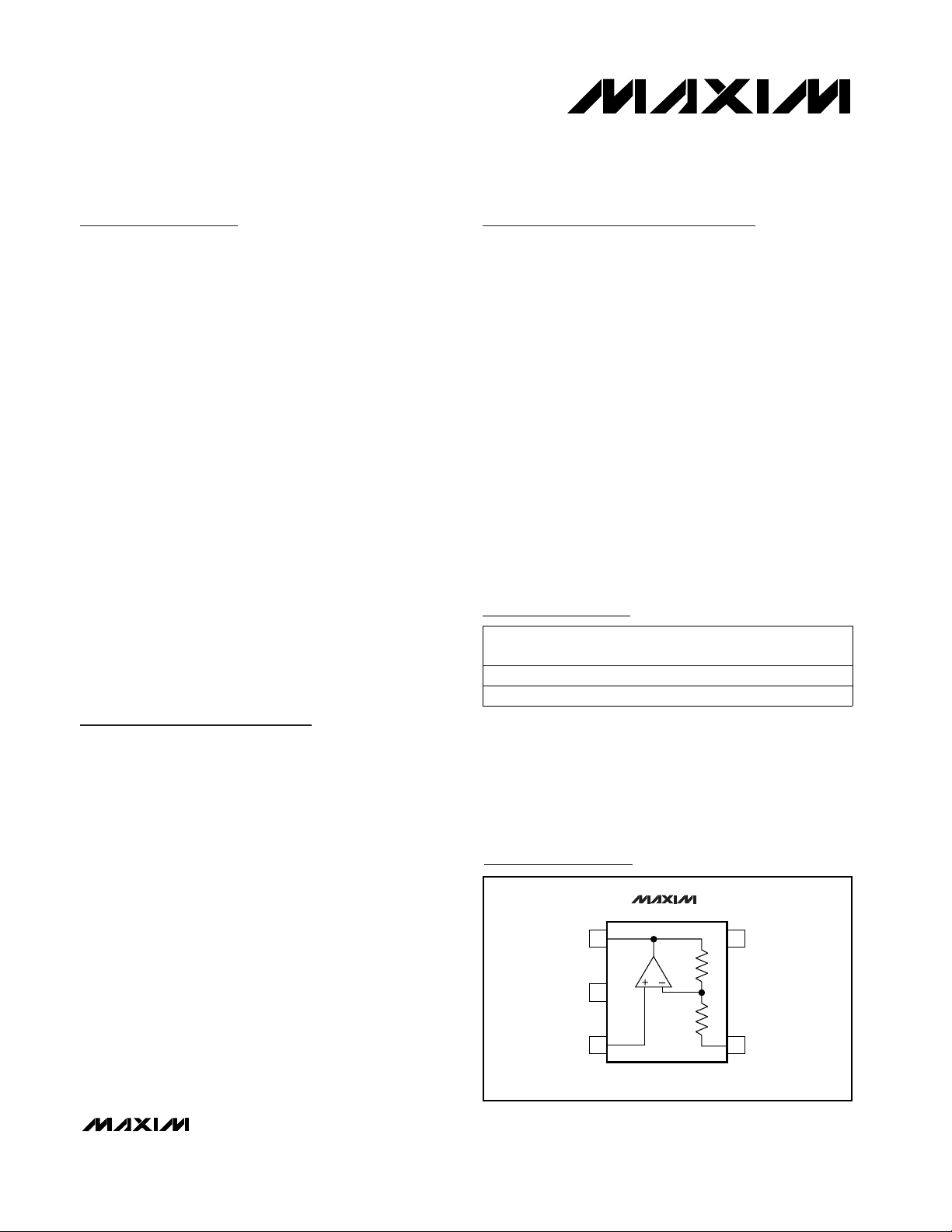
Pin Configurations/
Functional Diagrams
†
Patent pending.
GainAmp is a trademark of Maxim Integrated Products.
Rail-to-Rail is a registered trademark of Nippon Motorola, Ltd.
Ordering Information
Pin Configurations continued at end of data sheet.
Ordering Information continued at end of data sheet.
Note: Insert the desired gain code in the blank to complete the
part number (see the Gain Selector Guide).
**See the Gain Selector Guide for a list of preferred gains and
top marks.
8 SO
5 SOT23-5
PIN-
PACKAGE
TEMP. RANGE
-40°C to +70°C
-40°C to +70°CMAX4074__ESA
MAX4074__EUK-T
PART
—
**
TOP
MARK
Typical Operating Circuit appears at end of data sheet.
Gain Selector Guide appears at end of data sheet.
TOP VIEW
MAX4074
1
OUT
2
V
EE
3
IN+
SOT23-5
5
V
CC
R
F
R
G
4
IN-
Page 2
MAX4074–MAX4078
Micropower, SOT23, Rail-to-Rail,
Fixed-Gain, GainAmp/Open-Loop Op Amps
2 _______________________________________________________________________________________
ABSOLUTE MAXIMUM RATINGS
ELECTRICAL CHARACTERISTICS—MAX4074/MAX4075
(VCC= +2.5V to +5.5V, VEE= 0, V
IN+
= V
IN-
= VCC/2, RL= ∞ to VCC/2, TA= T
MIN
to T
MAX
, unless otherwise noted. Typical values
are at V
CC
= +5V and TA= +25°C.) (Note 1)
Stresses beyond those listed under “Absolute Maximum Ratings” may cause permanent damage to the device. These are stress ratings only, and functional
operation of the device at these or any other conditions beyond those indicated in the operational sections of the specifications is not implied. Exposure to
absolute maximum rating conditions for extended periods may affect device reliability.
Supply Voltages (VCCto VEE) ..................................-0.3V to +6V
Voltage Inputs (IN_)
MAX4076/MAX4077/MAX4078 .....(V
CC
+ 0.3V) to (VEE- 0.3V)
MAX4074/MAX4075..........................................................±17V
Output Short-Circuit Duration to Either Supply (OUT_). . . . Continuous
Continuous Power Dissipation (T
A
= +70°C)
5-Pin SOT23 (derate 7.1mW/°C above +70°C) ............571mW
14-Pin TSSOP (derate 6.3mW/°C above +70°C) ..........500mW
8-Pin µMAX (derate 4.1mW/°C above +70°C) ..............330mW
8-Pin SO (derate 5.88mW/°C above +70°C).................471mW
14-Pin SO (derate 8.33mW/°C above +70°C)...............667mW
Operating Temperature Range ...........................-40°C to +85°C
Junction Temperature......................................................+150°C
Storage Temperature Range .............................-65°C to +150°C
Lead Temperature (soldering, 10sec) .............................+300°C
Supply Current (per amplifier) I
CC
34 50
µA
VCC= 3V
PARAMETER SYMBOL MIN TYP MAX UNITS
Inverting Input Resistance R
IN_
80
kΩ
VCC- V
OH
300
Input Bias Current (Note 2) I
IN+_
0.8 1000 pA
Input Offset Voltage Drift 0.3 µV/°C
Noninverting Input Resistance R
IN_+
1000 MΩ
Negative Input Voltage Range IN_- ±1 5 V
Power-Supply Rejection Ratio PSRR 70 96 dB
Supply Voltage Range V
CC
2.5 5.5 V
300 1000
37 55
Input Offset Voltage V
OS
0.2 3.5 mV
Closed-Loop Output Impedance R
OUT
0.2 Ω
VCC- V
OH
5
Output Short-Circuit Current
-22
mA
0.5 2.5
VOL- V
EE
Output Voltage Swing (Note 4)
100 600
mV
RL= 1kΩ
VCC- V
OH
25 150
VOL- V
EE
Positive Input Voltage Range IN_+
11 80
RL= 10kΩ
VOL- V
EE
CONDITIONS
AV≥ +25V/V
Shorted to V
CC
AV< +25V/V
Shorted to V
EE
VEE-V
CC
-
0.15 1.2
Guaranteed by functional test (Note 3)
VCC= 2.5V to 5.5V
VGuaranteed by functional test (Note 3)
0.4 2.5
Guaranteed by PSRR test
VCC= 5V
RL= 1MΩ
RL= 1MΩ
Page 3
MAX4074–MAX4078
Micropower, SOT23, Rail-to-Rail,
Fixed-Gain, GainAmp/Open-Loop Op Amps
_______________________________________________________________________________________ 3
ELECTRICAL CHARACTERISTICS—MAX4076/MAX4077/MAX4078
(VCC= +2.5V to +5.5V, VEE= 0, V
IN+
= V
IN-
= VCC/2, RL= ∞ to VCC/2, TA= T
MIN
to T
MAX
, unless otherwise noted. Typical values
are at V
CC
= +5V and TA= +25°C.) (Note 1)
ELECTRICAL CHARACTERISTICS—MAX4074/MAX4075 (continued)
(VCC= +2.5V to +5.5V, VEE= 0, V
IN+
= V
IN-
= VCC/2, RL= ∞ to VCC/2, TA= T
MIN
to T
MAX
, unless otherwise noted. Typical values
are at V
CC
= +5V and TA= +25°C.) (Note 1)
90
80
90
-3dB Bandwidth BW (-3dB)
120
kHz
AV= +3V/V
AV= +5V/V
AV= +10V/V
AV= +25V/V
200AV= +1.25V/V
Input Noise Current Density 500
fA/√Hz
Capacitive Load Stability C
LOAD
500 pF
DC Gain Accuracy
0.01 1.0
%
f = 5kHz
No sustained oscillations
PARAMETER SYMBOL MIN TYP MAX UNITS
Power-Up Time 9 ms
Slew Rate SR 100 V/ms
Settling Time (to 0.01%) 60 µs
Input Voltage Noise Density e
n
150
nV/√Hz
CONDITIONS
Output settling to 1%
V
OUT
= 4V step
V
OUT
= 4V step
f = 5kHz (Note 5)
1.2
TA= +25°C
(VEE+ 25mV) < V
OUT
< (VCC- 25mV),
RL= 1MΩ (Note 6)
TA= T
MIN
to T
MAX
Supply Current (per amplifier) I
CC
40 55
µA
VCC= 3V
PARAMETER SYMBOL MIN TYP MAX UNITS
Input Bias Current (Note 2) I
IBIAS
1200pA
Input Offset Voltage Drift 1.5µV µV/°C
Power-Supply Rejection Ratio PSRR 70 95 dB
Supply Voltage Range V
CC
2.5 5.5 V
80 93
45 60
Input Offset Voltage V
OS
1.2 3.5mV mV
Closed-Loop Output Impedance R
OUT
0.2 Ω
4.5
Output Short-Circuit Current
20
mA
80 117
Large-Signal Voltage Gain A
VOL
dB
0.25V < V
OUT
< (VCC- 0.3V), RL= 5kΩ
80 95
Common-Mode Input Voltage
Range
I
VR
0.25V < V
OUT
< (VCC- 0.3V), RL= 10kΩ
CONDITIONS
AV= +1V/V
Shorted to V
CC
Shorted to V
EE
0.15 V
CC -
1.2
VCC= 2.5V to 5.5V
VGuaranteed by CMRR
Guaranteed by PSRR test
VCC= 5V
0.05V < V
OUT
< (VCC- 0.1V), RL= 1MΩ
RL= 1MΩ
Input Offset Current I
OS
±0.4 pA
Common-Mode Rejection Ratio CMRR 70 95 dB(VCC- 1.2V) ≥ VCM≥ -0.15V
Page 4
MAX4074–MAX4078
Micropower, SOT23, Rail-to-Rail,
Fixed-Gain, GainAmp/Open-Loop Op Amps
4 _______________________________________________________________________________________
ELECTRICAL CHARACTERISTICS—MAX4076/MAX4077/MAX4078 (continued)
(VCC= +2.5V to +5.5V, VEE= 0, V
IN+
= V
IN-
= VCC/2, RL= ∞ to VCC/2, TA= T
MIN
to T
MAX
, unless otherwise noted. Typical values
are at V
CC
= +5V and TA= +25°C.) (Note 1)
RL= 1MΩ
0.22 2.5
CONDITIONS
VOL- V
EE
RL= 10kΩ
750VOL- V
EE
12 50VCC- V
OH
RL= 5kΩ
mV
100 100
VOH/V
OL
Output Voltage Swing
VOL- V
EE
0.23 2.5
VCC- V
OH
100 100VCC- V
OH
kHzGBWGain-Bandwidth Product
UNITSMIN TYP MAXSYMBOLPARAMETER
230
V
OUT
= 4V step V/msSRSlew Rate 90
V
OUT
= 4V step µsSettling Time (to 0.01%) 69
f = 5kHz
nV/√Hz
e
n
Input Voltage Noise Density 110
f = 5kHz
fA/√Hz
Input Noise Current Density 1.1
No sustained oscillations, AV= +1V/V pFC
LOAD
Capacitive Load Stability 100
Note 1: All devices are 100% production tested at TA= +25°C. All temperature limits are guaranteed by design.
Note 2: Guaranteed by design.
Note 3: The input common-mode range for IN_+ is guaranteed by a functional test. A similar test is done on the IN_- input. See the
Applications Information section for more information on the input voltage range of the GainAmps.
Note 4: For A
V
= -0.5V/V and AV= -0.25V/V, the output voltage swing may be limited by the input voltage range.
Note 5: Includes noise from on-chip resistors.
Note 6: The gain accuracy test is performed with the GainAmps in the noninverting configuration. The output voltage swing is limit-
ed by the input voltage range for certain gains and supply voltage conditions. For situations where the output voltage swing
is limited by the valid input range, the output limits are adjusted accordingly.
Output settling to 1% msPower-Up Time 10
3
-6
1k 1M100k10k
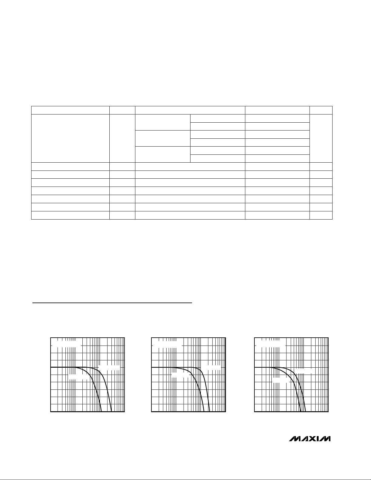
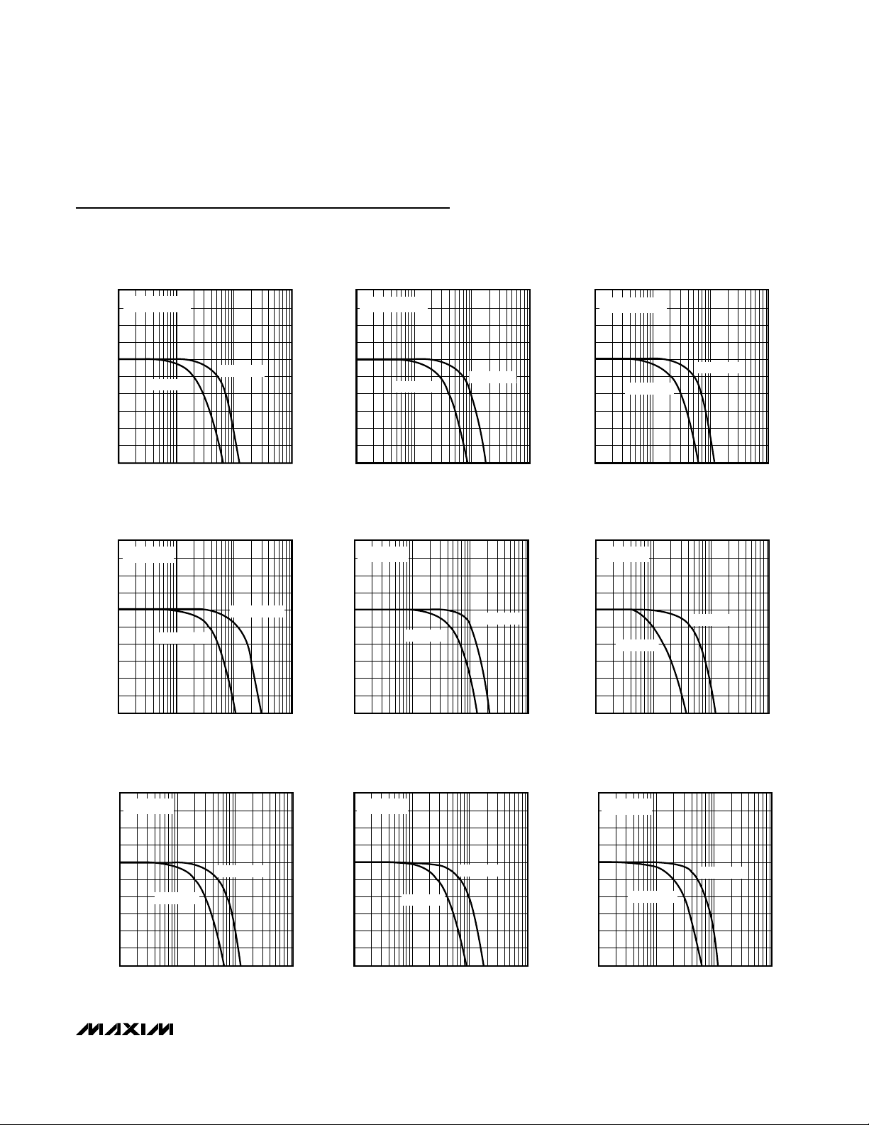
SMALL-SIGNAL GAIN vs. FREQUENCY
-3
-5
1
-1
4
-2
-4
2
0
MAX4074-8 tocc1-2
FREQUENCY (Hz)
GAIN (dB)
AV = +2.25V/V
AV = +1.25V/V
V
OUT
= 100mVp-p
3
-6
1k 1M10k 100k
SMALL-SIGNAL GAIN vs. FREQUENCY
-3
-5
1
-1
4
-2
-4
2
0
MAX4074-8 tocc3-4
FREQUENCY (Hz)
GAIN (dB)
AV = +4V/V
AV = +2.5V/V
V
OUT
= 100mVp-p
3
-6
1k 1M10k 100k
SMALL-SIGNAL GAIN vs. FREQUENCY
-3
-5
1
-1
4
-2
-4
2
0
MAX4074-8 tocc5-6
FREQUENCY (Hz)
GAIN (dB)
AV = +9V/V
AV = +5V/V
V
OUT
= 100mVp-p
Typical Operating Characteristics
(VCC= +5.0V, RL= 100kΩ to VCC/2, TA= +25°C, unless otherwise noted.)
MAX4074/MAX4075
Page 5
MAX4074–MAX4078
Micropower, SOT23, Rail-to-Rail,
Fixed-Gain, GainAmp/Open-Loop Op Amps
_______________________________________________________________________________________ 5
Typical Operating Characteristics
(VCC= +5.0V, RL= 100kΩ to VCC/2, TA= +25°C, unless otherwise noted.)
MAX4074/MAX4075
3
-6
1k 1M100k10k
LARGE-SIGNAL GAIN vs. FREQUENCY
-3
-5
1
-1
4
-2
-4
2
0
MAX4074-8 toc10
FREQUENCY (Hz)
GAIN (dB)
AV = +10V/V
AV = +21V/V
V
OUT
= 1Vp-p
3
-6
1k 1M100k10k
LARGE-SIGNAL GAIN vs. FREQUENCY
-3
-5
1
-1
4
-2
-4
2
0
MAX4074-8 toc11
FREQUENCY (Hz)
GAIN (dB)
AV = +25V/V
AV = +50V/V
V
OUT
= 1Vp-p
3
-6
1k 1M100k10k
LARGE-SIGNAL GAIN vs. FREQUENCY
-3
-5
1
-1
4
-2
-4
2
0
MAX4074-8 toc12
FREQUENCY (Hz)
GAIN (dB)
AV = +51V/V
AV = +101V/V
V
OUT
= 1Vp-p
SMALL-SIGNAL GAIN vs. FREQUENCY
4
V
= 100mVp-p
OUT
3
2
1
0
-1
GAIN (dB)
-2
-3
-4
-5
-6
AV = +21V/V
1k 1M100k10k
FREQUENCY (Hz)
LARGE-SIGNAL GAIN vs. FREQUENCY
4
V
= 1Vp-p
OUT
3
2
1
0
-1
GAIN (dB)
-2
-3
-4
-5
-6
1k 1M100k10k
AV = +2.25V/V
FREQUENCY (Hz)
MAX4074-8 toc04
AV = +10V/V
GAIN (dB)
MAX4074-8 toc07
AV = +1.25V/V
GAIN (dB)
SMALL-SIGNAL GAIN vs. FREQUENCY
4
V
= 100mVp-p
OUT
3
2
1
0
-1
-2
-3
-4
-5
-6
1k 1M100k10k
AV = +50V/V
FREQUENCY (Hz)
LARGE-SIGNAL GAIN vs. FREQUENCY
4
V
= 1Vp-p
OUT
3
2
1
0
-1
-2
-3
-4
-5
-6
1k 1M100k10k
AV = +4V/V
FREQUENCY (Hz)
AV = +25V/V
AV = +2.5V/V
MAX4074-8 toc05
GAIN (dB)
MAX4074-8 toc08
GAIN (dB)
SMALL-SIGNAL GAIN vs. FREQUENCY
4
V
= 100mVp-p
OUT
3
2
1
0
-1
-2
-3
-4
-5
-6
1k 1M100k10k
AV = +101V/V
FREQUENCY (Hz)
AV = +51V/V
LARGE-SIGNAL GAIN vs. FREQUENCY
4
V
= 1Vp-p
OUT
3
2
1
0
-1
-2
-3
-4
-5
-6
1k 1M100k10k
AV = +9V/V
AV = +5V/V
FREQUENCY (Hz)
MAX4074-8 toc06
MAX4074-8 toc09
Page 6
MAX4074–MAX4078
Micropower, SOT23, Rail-to-Rail,
Fixed-Gain, GainAmp/Open-Loop Op Amps
6 _______________________________________________________________________________________
Typical Operating Characteristics (continued)
(VCC= +5.0V, RL= 100kΩ to VCC/2, TA= +25°C, unless otherwise noted.)
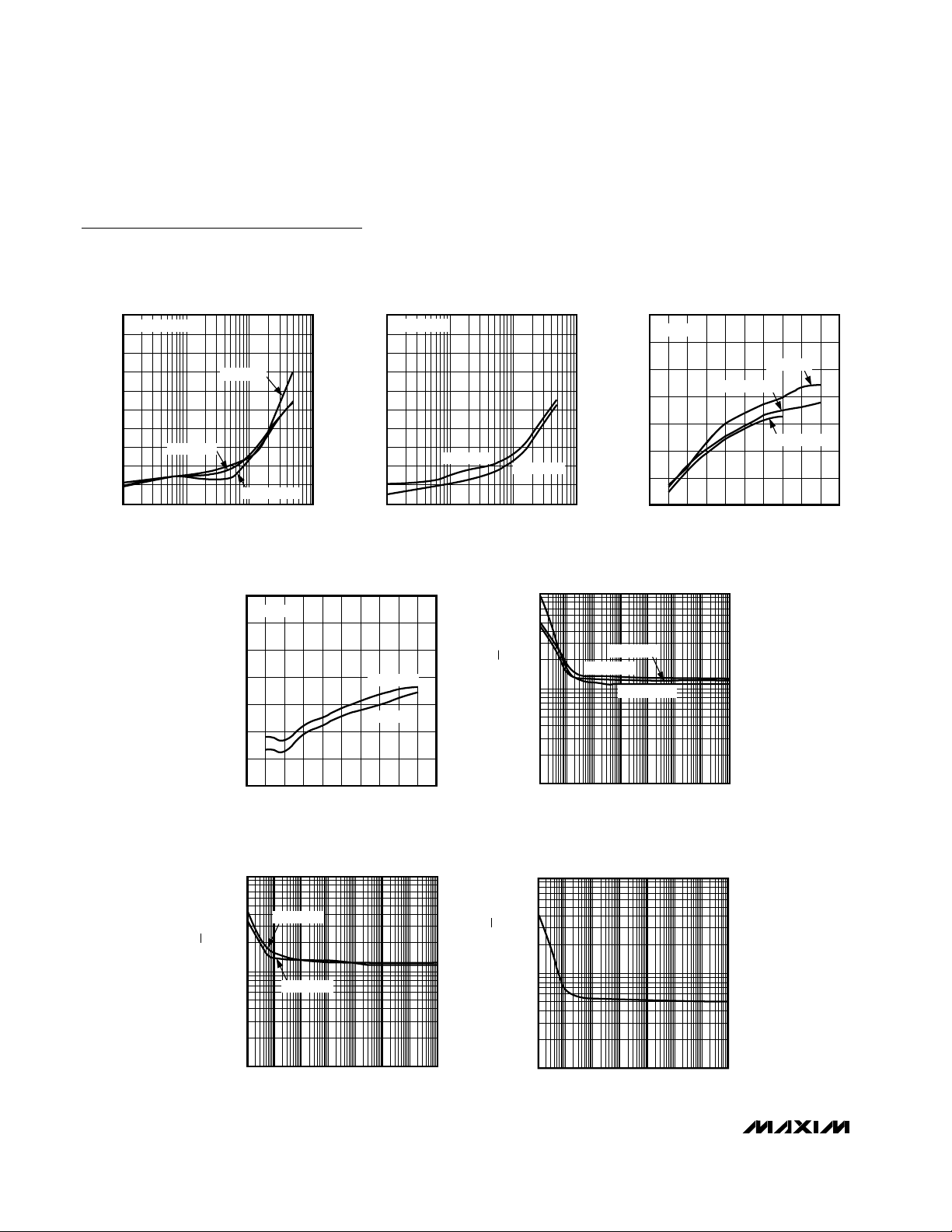
MAX4074/MAX4075
10
0.1
1 1k 10k 100k10 100 10M1M
CURRENT NOISE DENSITY
vs. FREQUENCY
1
MAX4074 TOC31
FREQUENCY (Hz)
CURRENT NOISE DENSITY (fA/√Hz)
TOTAL HARMONIC DISTORTION
0
V
= 1Vp-p
OUT
-10
-20
-30
-40
-50
-60
-70
-80
-90
-100
100 100k10k1k
vs. FREQUENCY
AV = +51V/V
FREQUENCY (Hz)
AV = +25V/V
MAX4074-8 toc26
TOTAL HARMONIC DISTORTION
vs. OUTPUT VOLTAGE SWING
-20
f = 10kHz
-30
-40
-50
THD (dB)
-60
-70
-80
-90
0 2.01.0 3.0 4.00.5 2.51.5 3.5 4.5 5.0
0
-10
-20
-30
-40
-50
THD (dB)
-60
-70
-80
-90
-100
100 100k10k1k
TOTAL HARMONIC DISTORTION
vs. FREQUENCY
V
= 1Vp-p
OUT
AV = +3V/V
AV = +10V/V
AV = +1.25V/V
FREQUENCY (Hz)
MAX4074-8 toc25
THD (dB)
TOTAL HARMONIC DISTORTION
vs. OUTPUT VOLTAGE SWING
-20
f = 10kHz
-30
-40
-50
THD (dB)
-60
-70
-80
-90
0 2.01.0 3.0 4.00.5 2.51.5 3.5 4.5 5.0
VOLTAGE SWING (Vp-p)
AV = +51V/V
AV = +25V/V
1000
MAX4074-8 toc28
100
VOLTAGE NOISE (nV/√Hz)
10
VOLTAGE NOISE DENSITY
vs. FREQUENCY
AV = +3V/V
AV = +10V/V
AV = +1.25V/V
1 1k 10k 100k10 100 1M 10M
FREQUENCY (Hz)
AV = +3V/V
AV = +10V/V
AV = +1.25V/V
VOLTAGE SWING (Vp-p)
MAX4074-8 toc29
MAX4074-8 toc27
VOLTAGE NOISE DENSITY
vs. FREQUENCY
1000
AV = +25V/V
100
VOLTAGE NOISE (nV/√Hz)
10
AV = +51V/V
1 1k 10k 100k10 100 1M 10M
FREQUENCY (Hz)
MAX4074-8 toc30
Page 7

MAX4074–MAX4078
Micropower, SOT23, Rail-to-Rail,
Fixed-Gain, GainAmp/Open-Loop Op Amps
_______________________________________________________________________________________ 7
Typical Operating Characteristics (continued)
(VCC= +5.0V, RL= 100kΩ to VCC/2, TA= +25°C, unless otherwise noted.)
MAX4074/MAX4075
MAX4074 TOC36
= +1.25V/V
A
V
50mV/div
= +1.25V/V
A
V
50mV/div
A
V
50mV/div
A
V
SMALL-SIGNAL PULSE RESPONSE
INPUT
OUTPUT
OUTPUT
= +3V/V
OUTPUT
= +5V/V
INPUT
OUTPUT
500mV/div
OUTPUT
500mV/div
= +3V/V
A
V
OUTPUT
500mV/div
= +5V/V
A
V
LARGE-SIGNAL PULSE RESPONSE
MAX4074 TOC35
OUTPUT
50mV/div
= +10V/V
A
V
OUTPUT
50mV/div
= +25V/V
A
V
OUTPUT
50mV/div
= +51V/V
A
V
OUTPUT
500mV/div
= +10V/V
A
V
OUTPUT
500mV/div
= +25V/V
A
V
OUTPUT
500mV/div
= +51V/V
A
V
10µs/div
10µs/div
Page 8

MAX4074–MAX4078
Micropower, SOT23, Rail-to-Rail,
Fixed-Gain, GainAmp/Open-Loop Op Amps
8 _______________________________________________________________________________________
Typical Operating Characteristics (continued)
(VCC= +5.0V, RL= 100kΩ to VCC/2, TA= +25°C, unless otherwise noted.)
300
0
1 10 100
OUTPUT VOLTAGE SWING
vs. R
LOAD
50
200
100
150
250
MAX4074 TOC34
R
LOAD
(kΩ)
OUTPUT SWING (mV)
V
CC
- V
OH
V
OL
- V
EE
100 1k 10k 100k 1M
OUTPUT IMPEDANCE
vs. FREQUENCY
MAX4074TOC33
FREQUENCY (Hz)
OUTPUT IMPEDANCE (Ω)
1k
0.1
1
10
100
-10
-100
100 100k10k1k
POWER-SUPPLY REJECTION
vs. FREQUENCY
-70
-90
-30
-50
0
-60
-80
-20
-40
MAX4074 TOC32
FREQUENCY (Hz)
PSR (dB)
VOH AND VOL vs. TEMPERATURE
175
150
125
100
75
50
25
VOLTAGE (mV)
0
-25
-50
-75
-100
-50 -5 10-35 -20 25 40 55 70 85
VOH, RL = 10kΩ
VOL, RL = 10kΩ
INPUT OFFSET VOLTAGE vs. TEMPERATURE
100
75
50
25
0
-25
-50
INPUT OFFSET VOLTAGE (µV)
-75
-100
- VEE = 2.5V)
(V
CC
VOH, RL = 1kΩ
VOL, RL = 1kΩ
TEMPERATURE (°C)
V
- V
= 5.5V
CC
EE
V
- V
= 2.5V
CC
EE
-50 -5 10-35 -20 25 40 55 70 85
TEMPERATURE (°C)
VOH AND VOL vs. TEMPERATURE
450
400
350
MAX4074/5-toc37
300
250
VOH, RL = 100kΩ
VOL, RL = 100kΩ
200
150
100
VOLTAGE (mV)
50
0
-50
-100
-150
-50 -5 10-35 -20 25 40 55 70 85
MAX4074/5-toc35
- VEE = 5.5V)
(V
CC
VOH, RL = 10kΩ
VOL, RL = 10kΩ
VOL, RL = 1kΩ
TEMPERATURE (°C)
INPUT BIAS CURRENT vs. TEMPERATURE
600
500
400
300
200
100
INPUT BIAS CURRENT (pA)
0
-100
-200
-45 0 15-30 -15 30 45 60 75 90
VOH, RL = 1kΩ
VOH, RL = 100kΩ
VOL, RL = 100kΩ
MAX4074/4075
V
- V
CC
MAX4076/77/78
TEMPERATURE (°C)
40.0
MAX4074/5-toc38
37.5
35.0
SUPPLY CURRENT (µA)
32.5
30.0
V
- V
= 5.5V
CC
EE
MAX4074/5-toc36
= 2.5V
EE
V
- V
= 5.5V
CC
EE
V
- V
= 2.5V
CC
EE
SUPPLY CURRENT vs. TEMPERATURE
V
- V
= 5.5V
CC
EE
V
- V
= 4.0V
CC
EE
V
- V
= 3.0V
CC
EE
V
- V
= 2.5V
CC
EE
-50 -5 10-35 -20 25 40 55 70 85
TEMPERATURE (°C)
MAX4074/5-toc39
Page 9

MAX4074–MAX4078
Micropower, SOT23, Rail-to-Rail,
Fixed-Gain, GainAmp/Open-Loop Op Amps
_______________________________________________________________________________________ 9
Typical Operating Characteristics (continued)
(VCC= +5.0V, RL= 100kΩ to VCC/2, TA= +25°C, unless otherwise noted.)
MAX4076/MAX4077/MAX4078
SMALL-SIGNAL GAIN vs. FREQUENCY
4
3
2
1
0
-1
GAIN (dB)
-2
-3
-4
-5
-6
1k 1M 10M100k10k
FREQUENCY (Hz)
CURRENT NOISE vs. FREQUENCY
100
10
1
CURRENT NOISE (pA/√Hz)
0.1
1 1k 10k 100k10 100 1M 10M
FREQUENCY (Hz)
MAX4078
ALL HOSTILE CROSSTALK vs. FREQUENCY
-60
THREE AMPLIFIERS DRIVEN,
-65
ONE OUTPUT MEASURED.
-70
-75
-80
-85
-90
CROSSTALK (dB)
-95
-100
-105
-110
1k 1M10k 100k
FREQUENCY (Hz)
MAX4076/7/8 toc1
MAX4076-8 toc4
MAX4076-8 toc7
LARGE-SIGNAL GAIN vs. FREQUENCY
4
3
2
1
0
-1
GAIN (dB)
-2
-3
-4
-5
-6
1k 1M 10M100k10k
FREQUENCY (Hz)
TOTAL HARMONIC DISTORTION
vs. FREQUENCY
-40
AV = +1V/V
-50
-60
THD (dB)
-70
-80
-90
100 100k10k1k
FREQUENCY (Hz)
GAIN AND PHASE
vs. FREQUENCY
120
80
40
0
-40
GAIN (dB)
-80
-120
-160
-200
PHASE
1 1k 10k 100k10 100 10M1M
FREQUENCY (Hz)
GAIN
MAX4076-8 toc8
MAX4076- 8 toc2
MAX4076-8 toc5
270
180
90
0
-90
-180
-270
-360
-450
VOLTAGE NOISE vs. FREQUENCY
1k
100
VOLTAGE NOISE (nV/√Hz)
10
1 1k 10k 100k10 100 1M 10M
FREQUENCY (Hz)
MAX4077
CROSSTALK vs. FREQUENCY
-80
-85
-90
-95
-100
-105
-110
CROSSTALK (dB)
-115
-120
-125
-130
1k 1M10k 100k
FREQUENCY (Hz)
COMMON-MODE REJECTION
vs. FREQUENCY
-10
-20
-30
-40
-50
-60
CMR (dB)
-70
PHASE (degrees)
-80
-90
-100
1 1k 10k 100k10 100 10M1M
FREQUENCY (Hz)
MAX4076-8 toc3
MAX4076-8 toc6
MAX4076-8 toc9
Page 10

MAX4074–MAX4078
Micropower, SOT23, Rail-to-Rail,
Fixed-Gain, GainAmp/Open-Loop Op Amps
10 ______________________________________________________________________________________
Pin Description
_______________Detailed Description
Maxim’s GainAmp fixed-gain amplifiers combine a lowcost rail-to-rail op amp with internal gain-setting resistors. Factory-trimmed on-chip resistors provide 0.1%
gain accuracy while decreasing design size, cost, and
layout. There are two versions in this amplifier family:
single/dual/quad open-loop, unity-gain-stable devices
(MAX4076/MAX4077/MAX4078), and single/dual fixedgain devices (MAX4074/MAX4075). All amplifiers feature rail-to-rail outputs and drive a 10kΩ load while
maintaining excellent DC accuracy.
Open-Loop Op Amps
The single/dual/quad MAX4076/MAX4077/MAX4078 are
low-power, open-loop op amps with rail-to-rail outputs.
These devices are compensated for unity-gain stability
and feature a GBW product of 230kHz. The commonmode range extends from 150mV below the negative
rail to within 1.2V of the positive rail. These high-performance op amps serve as the core for this family of
GainAmp fixed-gain amplifiers. Although the -3dB bandwidth will not correspond to that of a fixed-gain amplifier
in higher gain configurations, these open-loop op amps
can be used to prototype designs.
Internal Gain-Setting Resistors
Maxim’s proprietary laser trimming techniques allow
RF/RGvalues (Figure 1) that produce many different
gain configurations. These GainAmp fixed-gain amplifiers feature a negative-feedback resistor network that
is laser trimmed to provide a gain-setting feedback
ratio (RF/RG) with 0.1% typical accuracy. The standard
op amp pinouts allow the GainAmp fixed-gain amplifiers to plug directly into existing board designs, easily
replacing op amps-plus-resistor gain blocks.
Figure 1. Internal Gain-Setting Resistors
FUNCTION
Positive SupplyV
CC
5
No Connection. Not internally connected.N.C.—
Inverting Amplifier InputIN_-4
Noninverting Amplifier InputIN_+3
Negative Supply or GroundV
EE
2
Amplifier OutputOUT_1
7
1, 5, 8
2
3
4
6
8
—
2, 6
3, 5
4
1, 7
4
—
2, 6, 9, 13
3, 5, 10, 12
11
1, 7, 8, 14
MAX4075
MAX4077
MAX4078
µMAX/SO SO/TSSOPSOT23
NAME
SO
PIN
MAX4074/MAX4076
IN-
IN+
V
CC
R
G
V
EE
R
F
-R
F
A
=
V
R
G
AV = 1 +
R
R
F
G
OUT
Page 11

MAX4074–MAX4078
Micropower, SOT23, Rail-to-Rail,
Fixed-Gain, GainAmp/Open-Loop Op Amps
______________________________________________________________________________________ 11
GainAmp Bandwidth
GainAmp fixed-gain amplifiers feature factory-trimmed
precision resistors to provide fixed inverting gains from
-0.25V/V to -100V/V or noninverting gains from +1.25V/V
to +101V/V. The op amp core is decompensated strategically over the gain-set options to maximize bandwidth. Open-loop decompensation increases GBW
product, ensuring that usable bandwidth is maintained
with increasing closed-loop gains. A GainAmp with a
fixed gain of AV= +25V/V has a -3dB bandwidth of
120kHz. By comparison, a unity-gain-stable op amp configured for AV= +25V/V would yield a -3dB bandwidth
of only 8kHz. Decompensation is performed at five intermediate gain sets, as shown in the Gain Selector
Guide.
High-Voltage (±17V)
Input Fault Protection
The MAX4074/MAX4075 family includes ±17V input
fault protection. For normal operation, see the input
voltage range specification in the Electrical Character-
istics. Overdriven inputs up to ±17V will not cause output phase reversal. A back-to-back SCR structure at
the input pins allows either input to safely swing ±17V
relative to VEE(Figure 2). Additionally, the internal op
amp inputs are diode clamped to both supply rails for
the protection of sensitive input stage circuitry. Current
through the clamp diodes is limited by a 5kΩ resistor at
the noninverting input, and by RGat the inverting input.
An IN+ or IN- fault voltage as high as ±17V causes less
than 3.5mA to flow through the input pin, protecting
both the GainAmp and the signal source from damage.
Applications Information
GainAmp fixed-gain amplifiers offer a precision, fixedgain amplifier in a small package that can be used in a
variety of circuit board designs. GainAmp fixed-gain
amplifiers can be used in many op amp circuits that
use resistive negative feedback to set gain, and do not
require other connections to the op amp inverting input.
Both inverting and noninverting op amp configurations
can be implemented easily using a GainAmp.
GainAmp Input Voltage Range
The MAX4074/MAX4075 combine both an op amp and
gain-setting feedback resistors on the same IC. The
inverting input voltage range is different from the noninverting input voltage range because the inverting input
pin is connected to the RGinput series resistor. Just as
with a discrete design, take care not to saturate the
inputs/output of the core op amp to avoid signal distortions or clipping.
Figure 2. Input Protection
IN-
IN+
17V
SCR
V
17V
SCR
V
R
F
R
G
OUT
EE
EE
V
CC
5k
V
EE
NOTE: INPUT STAGE PROTECTION INCLUDES TWO 17V SCRs
AND TWO DIODES AT THE INPUT STAGE.
MAX4074
MAX4075
Page 12

MAX4074–MAX4078
Micropower, SOT23, Rail-to-Rail,
Fixed-Gain, GainAmp/Open-Loop Op Amps
12 ______________________________________________________________________________________
GainAmp Signal Coupling
and Configurations
Common op amp configurations include both noninverting and inverting amplifiers. Figures 3–6 show various
single- and dual-supply circuit configurations. In singlesupply systems, use a resistor-divider to bias the noninverting input. A lowpass filter capacitor from the op amp
input to ground (Figure 5) prevents high-frequency
power-supply noise from coupling into the op amp input.
Dual-supply systems can have ground-referenced signals DC-coupled into the inverting or noninverting inputs.
Supply Bypassing and Board Layout
All devices in this GainAmp family operate from a +2.5V
to +5.5V single supply or from ±1.25V to ±2.75V dual
supplies. For single-supply operation, bypass the power
supply with a 0.1µF capacitor to ground. For dual supplies, bypass each supply to ground. Bypass with
capacitors as close to the device as possible to minimize lead inductance and noise. A printed circuit board
with a low-inductance ground plane is recommended.
Capacitive-Load Stability
Driving large capacitive loads can cause instability in
most low-power, rail-to-rail output amplifiers. The fixedgain amplifiers of this GainAmp family are stable with
capacitive loads up to 100pF. Stability with higher
capacitive loads can be improved by adding an isolation resistor in series with the op amp output, as shown
in Figure 7. This resistor improves the circuit’s phase
margin by isolating the load capacitor from the amplifier’s output. In Figure 8, a 220pF capacitor is driven with
a 100Ω isolation resistor exhibiting some overshoot but
no oscillation. Figures 9 and 10 show the typical smallsignal pulse responses of GainAmp fixed-gain amplifiers with 47pF and 100pF capacitive loads and no
isolation resistor
Figure 3. Single-Supply, DC-Coupled Inverting Amplifier with
Negative Input Voltage
Figure 4. Dual-Supply, DC-Coupled Inverting Amplifier
Figure 5. Single-Supply, AC-Coupled Inverting Amplifier
Figure 6. Dual-Supply, DC-Coupled Noninverting Amplifier
V
CC
MAX4074
V
IN
R
G
V
CC
0.1µF
V
IN
R
G
V
IN
V
CC
MAX4074
V
CC
V
EE
R
F
MAX4074
V
CC
R
F
MAX4074
=
= V
= - V
V
IN
CC
(1+
RF
IN
(
- VIN
R
G
(
F
G
V
OUT
R
V
OUT
2 R
V
OUT
R
)
RF
)
)
G
V
EE
V
CC
R
V
IN
R
G
R
F
V
=
OUT
R
-R
F
)
(V
IN
G
R
G
F
Page 13

MAX4074–MAX4078
Micropower, SOT23, Rail-to-Rail,
Fixed-Gain, GainAmp/Open-Loop Op Amps
______________________________________________________________________________________ 13
Figure 7. Dual-Supply, Capacitive-Load-Driving Circuit
Figure 8. Small-Signal/Large-Signal Transient Response with
Excessive Capacitive Load and Isolation Resistor
MAX4074
INPUT
R
G
R
F
V
CC
R
ISO
C
V
EE
L
OUTPUT
R
L
INPUT
AV = +5V/V
50mV/div
A
= +5V/V
V
500mV/div
OUTPUT
OUTPUT
Page 14

MAX4074–MAX4078
Micropower, SOT23, Rail-to-Rail,
Fixed-Gain, GainAmp/Open-Loop Op Amps
14 ______________________________________________________________________________________
Figure 9. GainAmp Small-Signal Pulse Response (CL= 340pF,
R
L
= 100kΩ)
Figure 10. GainAmp Small-Signal Pulse Response (CL= 940pF,
R
L
= 100kΩ)
INPUT
OUTPUT
50mV/div
= +1.25V/V
A
V
OUTPUT
50mV/div
= +3V/V
A
V
OUTPUT
50mV/div
= +5V/V
A
V
OUTPUT
50mV/div
= +10V/V
A
V
50mV/div
= +1.25V/V
A
V
50mV/div
A
V
50mV/div
A
V
50mV/div
= +10V/V
A
V
INPUT
OUTPUT
OUTPUT
= +3V/V
OUTPUT
= +5V/V
OUTPUT
OUTPUT
50mV/div
= +25V/V
A
V
OUTPUT
50mV/div
= +51V/V
A
V
10µs/div
OUTPUT
50mV/div
= +25V/V
A
V
OUTPUT
50mV/div
= +51V/V
A
V
10µs/div
Page 15

MAX4074–MAX4078
Micropower, SOT23, Rail-to-Rail,
Fixed-Gain, GainAmp/Open-Loop Op Amps
______________________________________________________________________________________ 15
Gain Selector Guide
Note: Bold indicates preferred gains. These gain versions are available as samples and in small quantities.
1.25 200
NONINVERTING
GAIN (V/V)
ADJBAB
-3dB BW
(kHz)
GAIN
CODE
TOP MARK
INVERTING
GAIN (V/V)
0.25
1.5 136 ADJCAC 0.5
2.25 70 ADJEAE 1.25
2 102 ADJD
AD
1
3 135 ADJG
AG
2
4
2.5
90 ADJIAJ 3
3.5 116
180
ADJHAH 2.5
ADJFAF 1.5
6 71 ADJKAL 5
9
5
50 ADJMAN 8
7 61
80
ADJLAM 6
11 79 ADJO
BA
10
16
10
54 ADJQBC 15
13.5 64
90
ADJPBB 12.5
ADJN
AO
9
ADJJ
AK
4
25 120 ADJS
BE
24
21 40 ADJRBD 20
31 89 ADJUBG 30
50
26
50 ADJW
BJ
49
41 67
106
ADJVBH 40
ADJTBF 25
61 66 ADJYBL 60
100
51
40 ADKA
BN
99
80 50
82
ADJZBM 79
101 38 ADKB
CA
100
ADJX
BK
50
Page 16

MAX4074–MAX4078
Micropower, SOT23, Rail-to-Rail,
Fixed-Gain, GainAmp/Open-Loop Op Amps
16 ______________________________________________________________________________________
Pin Configurations/Functional Diagrams
TOP VIEW
N.C.
IN-
MAX4074
N.C.
1
2
-
8
V
7
CC
+
6
IN+
V
3
4
EE
OUT
N.C.
5
SO
MAX4075
OUTA
1
R
F
-
INA-
2
+
R
G
+
INA+
3
V
4
EE
8
V
CC
7
OUTB
R
F
-
6
INB-
R
G
INB+
5
µMAX/SO
OUT
OUTA
INA-
INA+
V
MAX4076
N.C.
1
2
-
8
V
7
CC
+
6
3
4
OUT
N.C.
5
SO
MAX4078
1
-
+
2
3
4
5
6
+
-
14
OUTD
-
+
13
IND-
12
IND+
V
11
EE
INC+
10
INC-
9
+
-
V
IN+
MAX4076
1
2
EE
3
+
5
V
-
4
IN-
N.C.
CC
IN-
IN+
SOT23-5
V
EE
MAX4077
1
-
2
+
+
3
4
EE
µMAX/SO
8
V
OUTA
CC
OUTB
INB-
INB+
INA-
INA+
V
INB+
INB-
CC
7
-
6
5
OUTB
7
SO/TSSOP
8
OUTC
Page 17

MAX4074–MAX4078
Micropower, SOT23, Rail-to-Rail,
Fixed-Gain, GainAmp/Open-Loop Op Amps
______________________________________________________________________________________ 17
___________________Chip Information
TRANSISTOR COUNTS
MAX4074: 180 MAX4077: 340
MAX4075: 360 MAX4078: 332
MAX4076: 180
Note: Insert the desired gain code in the blank to complete the
part number (see the Gain Selector Guide).
**See the Gain Selector Guide for a list of preferred gains and
top marks.
Ordering Information (continued)
MAX4074
INPUT
IN-
IN+
+5V
OUT
V
CC
V
CC
V
EE
V
CC
R
G
0.1µF
R
F
0.1µF
0.1µF
Typical Operating Circuit
MAX4075__ESA -40°C to +70°C 8 SO
MAX4075__EUA
-40°C to +70°C 8 µMAX
MAX4078ESD -40°C to +70°C 14 SO
MAX4078EUD
-40°C to +70°C 14 TSSOP
PART
MAX4076EUK-T
MAX4076ESA -40°C to +70°C
-40°C to +70°C
TEMP. RANGE
PIN-
PACKAGE
5 SOT23-5
8 SO
MAX4077EUA
MAX4077ESA -40°C to +70°C
-40°C to +70°C 8 µMAX
8 SO
—
—
—
—
TOP
MARK
**
—
—
—
Page 18

MAX4074–MAX4078
Micropower, SOT23, Rail-to-Rail,
Fixed-Gain, GainAmp/Open-Loop Op Amps
18 ______________________________________________________________________________________
Package Information
SOT5L.EPS
Page 19

MAX4074–MAX4078
Micropower, SOT23, Rail-to-Rail,
Fixed-Gain, GainAmp/Open-Loop Op Amps
______________________________________________________________________________________ 19
Package Information (continued)
TSSOP.EPS
Page 20

MAX4074–MAX4078
Micropower, SOT23, Rail-to-Rail,
Fixed-Gain, GainAmp/Open-Loop Op Amps
Maxim cannot assume responsibility for use of any circuitry other than circuitry entirely embodied in a Maxim product. No circuit patent licenses are
implied. Maxim reserves the right to change the circuitry and specifications without notice at any time.
20 ____________________Maxim Integrated Products, 120 San Gabriel Drive, Sunnyvale, CA 94086 408-737-7600
© 1999 Maxim Integrated Products Printed USA is a registered trademark of Maxim Integrated Products.
Package Information (continued)
8LUMAXD.EPS
SOICN.EPS
 Loading...