

Page 1
General Description
The single MAX4036/MAX4037 and dual MAX4038/
MAX4039 operational amplifiers operate from a single
+1.4V to +3.6V (without reference) or +1.8V to +3.6V (with
reference) supply and consume only 800nA of supply
current per amplifier, and 1.1µA for the optional reference. The MAX4036/MAX4038 feature a common-mode
input voltage range from 0V to VDD- 0.4V at VDD= 1.4V.
The MAX4037/MAX4039 feature a 1.232V voltage reference capable of sourcing 100µA and sinking 20µA.
The MAX4036–MAX4039s’ Rail-to-Rail®outputs drive
5kΩ loads to within 25mV of the rails. Ultra-low supply
current, low operating voltage, and rail-to-rail outputs
make the MAX4036–MAX4039 ideal for use in singlecell lithium-ion (Li+), or two-cell NiCd/NiMH/alkaline
battery-powered applications.
The MAX4036 is available in an SC70 package, the
MAX4037 in a SOT23 package, and the MAX4038/
MAX4039 in µMAX and TDFN packages. All devices
are specified over the -40°C to +85°C extended temperature range.
Applications
Battery-Powered/Solar-Powered Systems
Portable Medical Instrumentation
Pagers and Cell Phones
Micropower Thermostats and Potentiostats
Electrometer Amplifiers
Remote Sensor Amplifiers
Active Badges
pH Meters
Features
♦ Ultra-Low 800nA per Amplifier Supply Current
♦ Ultra-Low 1.4V Supply Voltage Operation (1.8V for
MAX4037/MAX4039)
♦ Rail-to-Rail Outputs Drive 5kΩ and 5000pF Load
♦ 1.232V ±0.5%, 80ppm/°C (max) Reference
(MAX4037/MAX4039)
♦ No External Reference Bypass Capacitor
Required
♦ No Phase Reversal for Overdriven Inputs
♦ Low 1.0pA (typ) Input Bias Current
♦ Low 200µV Input Offset Voltage
♦ Unity-Gain Stable
♦ Available in Tiny SC70, SOT23, TDFN, and µMAX
Packages
MAX4036–MAX4039
Low I
BIAS
, +1.4V/800nA, Rail-to-Rail Op Amps
with +1.2V Buffered Reference
________________________________________________________________ Maxim Integrated Products 1
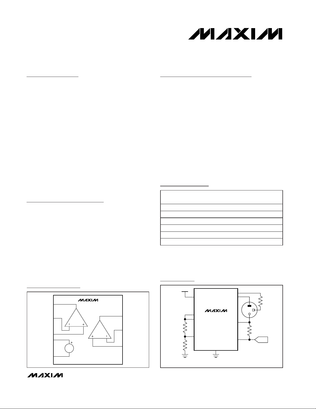
INA+
SENSOR
REF
THREE-ELECTRODE POTENTIOSTAT APPLICATION
INB+
OUTA
INB-
OUTB
INA-
V
DD
V
SS
MAX4039
3V
ADC
Typical Operating Circuit
Ordering Information
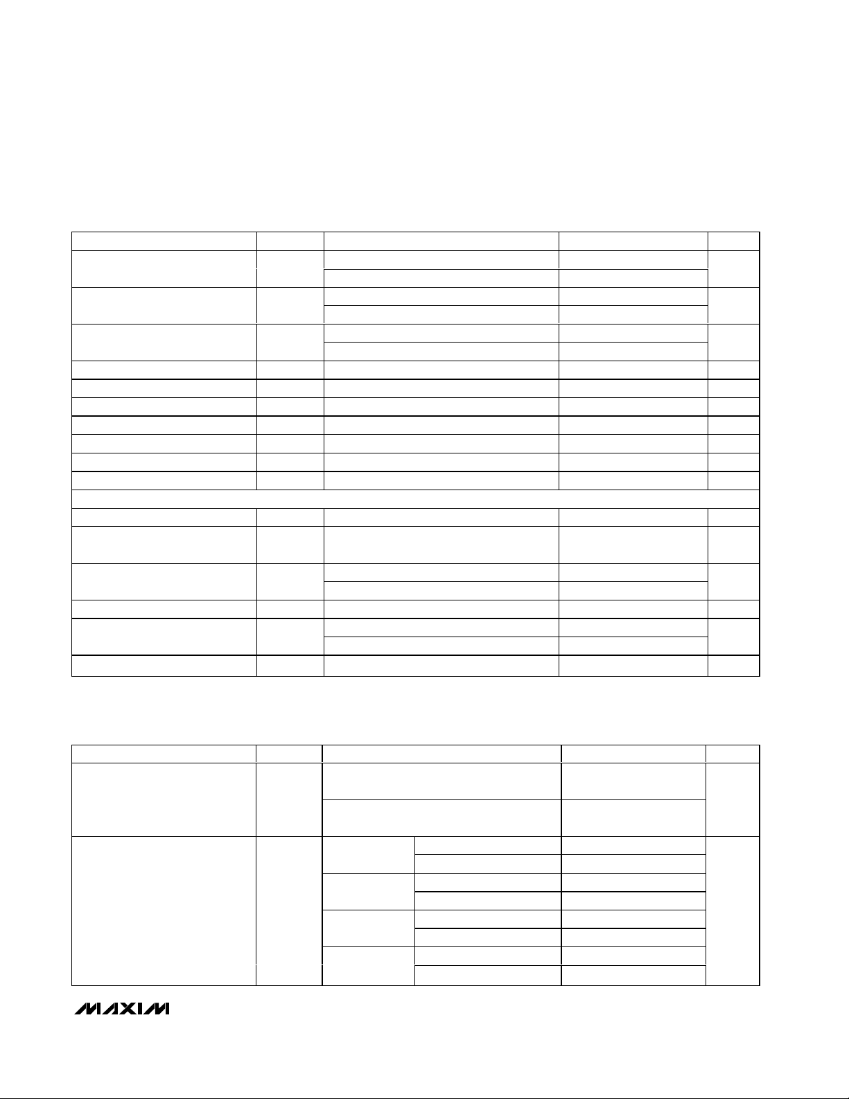
MAX4039
OUTA
REF
INA-
INA+
V
SS
OUTB
INB-
INB+
V
DD
REF
Functional Diagram
19-3142; Rev 0; 1/04
For pricing, delivery, and ordering information, please contact Maxim/Dallas Direct! at
1-888-629-4642, or visit Maxim’s website at www.maxim-ic.com.
*Future product—contact factory for availability.
**EP = Exposed paddle.
Rail-to-Rail is a registered trademark of Nippon Motorola, Ltd.
PART
TEMP RANGE
PINPACKAGE
TOP
MARK
MAX4036EXK-T*
5 SC70-5
AFR
MAX4037EUT-T
6 SOT23-6
ABRX
MAX4038ETA
AGO
MAX4038EUA
8 µMAX —
MAX4039ETB*
AAN
MAX4039EUB
10 µMAX —
Pin Configurations and Selector Guide appear at end of
data sheet.
-40°C to +85°C
-40°C to +85°C
-40°C to +85°C 8 TDFN-EP**
-40°C to +85°C
-40°C to +85°C 10 TDFN-EP**
-40°C to +85°C
Page 2
MAX4036–MAX4039
Low I
BIAS
, +1.4V/800nA, Rail-to-Rail Op Amps
with +1.2V Buffered Reference
2 _______________________________________________________________________________________
ABSOLUTE MAXIMUM RATINGS
ELECTRICAL CHARACTERISTICS
(VDD= +3V, VSS= VCM= 0V, V
OUT_
= VDD/2, RLto VDD/2, CL= 15pF, TA= +25°C, unless otherwise specified.)
Stresses beyond those listed under “Absolute Maximum Ratings” may cause permanent damage to the device. These are stress ratings only, and functional
operation of the device at these or any other conditions beyond those indicated in the operational sections of the specifications is not implied. Exposure to
absolute maximum rating conditions for extended periods may affect device reliability.
VDDto VSS.............................................................-0.3V to +4.0V
INA+, INB+, INA-, INB-, IN+, IN-, OUTA,
OUTB, OUT, REF .........................(V
SS
- 0.3V) to (VDD+ 0.3V)
OUTA, OUTB, OUT, REF Shorted to V
SS
or VDD.......Continuous
Maximum Continuous Power Dissipation (T
A
= +70°C)
5-Pin SC70 (derate 3.1mW/°C above +70°C)..............247mW
6-Pin SOT23 (derate 8.7mW/°C above +70°C)............696mW
8-Pin µMAX (derate 4.5mW/°C above +70°C) .............362mW
8-Pin TDFN (derate 24.4mW/°C above +70°C) .........1951mW
10-Pin µMAX (derate 5.6mW/°C above +70°C) ...........444mW
10-Pin TDFN (derate 24.4mW/°C above +70°C) .......1951mW
Operating Temperature Range ...........................-40°C to +85°C
Junction Temperature .....................................................+150°C
Storage Temperature Range .............................-65°C to +150°C
Lead Temperature (soldering, 10s) .................................+300°C
PARAMETER
CONDITIONS
UNITS
MAX4036/MAX4038, guaranteed by PSRR
tests
1.4 3.6
Supply Voltage Range V
DD
MAX4037/MAX4039, guaranteed by PSRR
and line regulation tests
1.8 3.6
V
VDD = 1.4V 0.8 1.2
MAX4036
V
DD
= 3.6V 0.9 1.3
VDD = 1.8V 1.9 2.4
MAX4037
V
DD
= 3.6V 2.0 2.5
VDD = 1.4V 1.7 2.3
MAX4038
V
DD
= 3.6V 1.9 2.5
VDD = 1.8V 2.8 4.0
Supply Current I
DD
MAX4039
V
DD
= 3.6V 3.0 4.1
µA
OPERATIONAL AMPLIFIERS
Input Offset Voltage V
OS
mV
Input Bias Current I
B
(Note 1)
±10 pA
Input Offset Current I
OS
(Note 1)
±20 pA
V
D D
= 1.4V
VDD -
0.4
VDD = 1.8V
VDD -
0.3
Input Common-Mode Voltage
Range
V
CM
Guaranteed by
CMRR test
V
DD
= 3.3V
VDD -
0.2
V
VDD = 1.4V, VSS † VCM † (VDD - 0.4V)
(MAX4036/MAX4038 only)
50 70
VDD = 1.8V, VSS † VCM † (VDD - 0.3V) 50 70
Common-Mode Rejection Ratio CMRR
V
DD
= 3.3V, VSS † VCM † (VDD - 0.2V) 56 76
dB
1.4V † VDD † 3.6V (MAX4036/MAX4038
only)
62 82
Power-Supply Rejection Ratio PSRR
1.8V † V
DD
† 3.6V 62 84
dB
SYMBOL
MIN TYP MAX
( M AX 4036/M AX 4038 onl y)
V
SS
V
SS
V
SS
±0.2 ±2.0
±1.0
±0.3
Page 3
MAX4036–MAX4039
Low I
BIAS
, +1.4V/800nA, Rail-to-Rail Op Amps
with +1.2V Buffered Reference
_______________________________________________________________________________________ 3
ELECTRICAL CHARACTERISTICS (continued)
(VDD= +3V, VSS= VCM= 0V, V
OUT_
= VDD/2, RLto VDD/2, CL= 15pF, TA= +25°C, unless otherwise specified.)
PARAMETER
SYMBOL
CONDITIONS
MIN
TYP
MAX
UNITS
80 108
Large-Signal Voltage Gain A
VOL
78 105
dB
RL = 100kΩ 25
Output Voltage Swing High
RL = 5kΩ 25 50
mV
RL = 100kΩ 25
Output Voltage Swing Low
RL = 5kΩ 25 50
mV
Output Short-Circuit Current I
SCO
To VDD or V
SS
mA
Gain-Bandwidth Product GBW 4 kHz
Phase Margin θ
M
90
Degrees
Slew Rate SR 0.4
V/ms
Power-On Time t
ON
(Note 3)
ms
Input Noise-Voltage Density e
n
f = 1kHz 500
nV/√Hz
Capacitive-Load Stability C
LOADAVCL
= 1V/V, no sustained oscillations
pF
REFERENCE (MAX4037/MAX4039)
Reference Voltage V
REF
V
Line Regulation
∆V
REF
/
∆V
DD
VDD = +1.8V to +3.6V 0.3 %/V
0 † I
LOAD
† 100µA, sourcing
Load Regulation
∆V
REF
/
∆I
LOAD -20µA † I
LOAD
† 0, sinking
%/µA
Reference Output Voltage Noise
e
n
0.1Hz to 10Hz 60
µV
P-P
Short to V
DD
Output Short-Circuit Current I
SCR
Short to V
SS
1.9
mA
Capacitive-Load Stability Range
C
LOAD
(Note 1) 0 250 pF
ELECTRICAL CHARACTERISTICS
(VDD= +3V, VSS= VCM= 0V, V
OUT_
= VDD/2, RLto VDD/2, CL= 15pF, TA= T
MIN
to T
MAX
, unless otherwise specified.) (Note 2)
PARAMETER
SYMBOL
CONDITIONS
MIN
TYP
MAX
UNITS
MAX4036/MAX4038, guaranteed by PSRR
test
1.4 3.6
Supply Voltage Range V
DD
MAX4037/MAX4039, guaranteed by PSRR
and line regulation tests
1.8 3.6
V
VDD = 1.4V 1.7
MAX4036
V
DD
= 3.6V 1.8
VDD = 1.8V 3.1
MAX4037
V
DD
= 3.6V 3.2
VDD = 1.4V 2.9
MAX4038
V
DD
= 3.6V 3.2
VDD = 1.8V 5.2
Supply Current I
DD
MAX4039
V
DD
= 3.6V 5.3
µA
RL = 100kΩ, 50mV † V
RL = 5kΩ, 150mV † V
VDD - V
OH
VOL - V
SS
† (VDD - 50mV)
OUT
† (VDD - 150mV)
OUT
±13
0.25
5000
1.226 1.232 1.238
0.0015
0.0075
0.25
Page 4
ELECTRICAL CHARACTERISTICS (continued)
(VDD= +3V, VSS= VCM= 0V, V
OUT_
= VDD/2, RLto VDD/2, CL= 15pF, TA= T
MIN
to T
MAX
, unless otherwise specified.) (Note 2)
PARAMETER
CONDITIONS
UNITS
OPERATIONAL AMPLIFIERS
Input Offset Voltage V
OS
±8 mV
Input Offset Voltage Temperature
Coefficient
TCV
OS
±1
µV/°C
Input Bias Current I
B
pA
Input Offset Current I
OS
pA
VDD = 1.4V
VDD -
0.4
VDD = 1.8V
VDD -
0.4
Input Common-Mode Voltage
Range
V
CM
Guaranteed by
CMRR test
V
DD
= 3.3V
VDD -
0.2
V
VDD = 1.4V, VSS ≤ VCM ≤ (VDD - 0.4V)
(MAX4036/MAX4038 only)
44
VDD = 1.8V, VSS ≤ VCM ≤ (VDD - 0.4V) 50
Common-Mode Rejection Ratio CMRR
V
DD
= 3.3V, VSS ≤ VCM ≤ (VDD - 0.2V) 52
dB
1.4V ≤ VDD ≤ 3.6V
(MAX4036/MAX4038 only)
60
Power-Supply Rejection Ratio PSRR
1.8V ≤ V
DD
≤ 3.6V 60
dB
RL = 100kΩ, 50mV ≤ V
OUT
≤ (VDD - 50mV) 75
Large-Signal Voltage Gain A
VOL
RL = 5kΩ, 150mV ≤ V
OUT
≤ (VDD - 150mV) 73
dB
RL = 100kΩ 10
Output Voltage Swing High
RL = 5kΩ
mV
RL = 100kΩ 10
Output Voltage Swing Low
RL = 5kΩ
mV
REFERENCE (MAX4037/MAX4039)
Reference Voltage Temperature
Coefficient
(Note 1) 20 80
ppm/°C
Line Regulation
∆V
REF
/
∆V
DD
VDD = 1.8V to 3.6V 0.6 %/V
0 ≤ I
LOAD
≤ 100µA, sourcing
Load Regulation
∆V
REF
/
-20µA ≤ I
LOAD
≤ 0, sinking
%/µA
Capacitive-Load Stability Range
C
LOAD
(Note 1) 0
pF
Note 1: Guaranteed by design.
Note 2: All devices are production tested at T
A
= +25°C. All temperature limits are guaranteed by design.
Note 3: Output settles within 1% of final value.
MAX4036–MAX4039
Low I
BIAS
, +1.4V/800nA, Rail-to-Rail Op Amps
with +1.2V Buffered Reference
4 _______________________________________________________________________________________
SYMBOL
V
- V
DD
OH
VOL - V
SS
TCV
REF
∆I
LOAD
(MAX4036/MAX4038 only)
MIN TYP MAX
V
SS
V
SS
V
SS
±100
±200
100
100
0.003
0.015
250
Page 5
MAX4036–MAX4039
Low I
BIAS
, +1.4V/800nA, Rail-to-Rail Op Amps
with +1.2V Buffered Reference
_______________________________________________________________________________________ 5
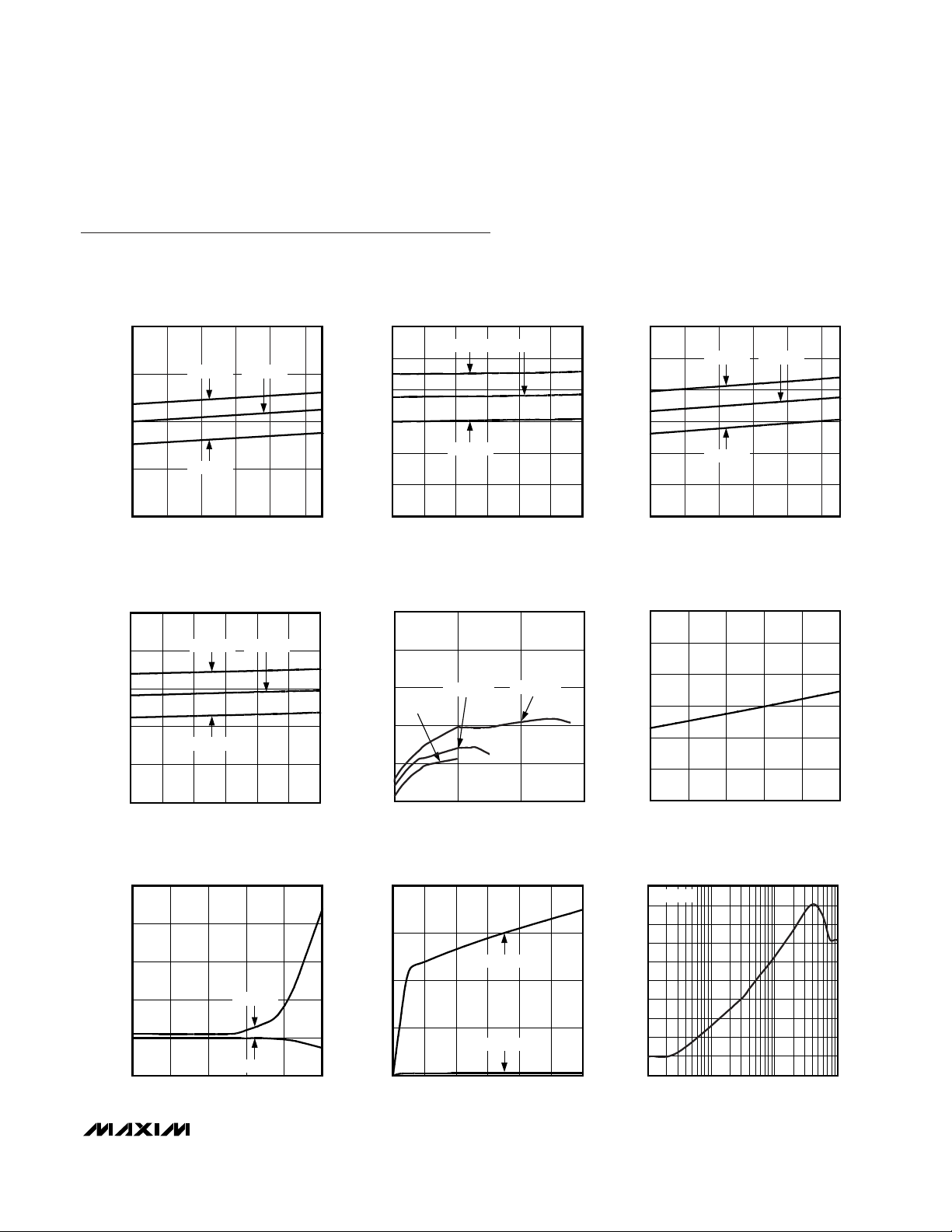
MAX4036
SUPPLY CURRENT
vs. SUPPLY VOLTAGE AND TEMPERATURE
MAX4036 toc01
SUPPLY VOLTAGE (V)
SUPPLY CURRENT (µA)
3.02.62.21.8
0.4
0.8
1.2
1.6
0
1.4 3.4
TA = +85°C
TA = -40°C
TA = +25°C
MAX4037
SUPPLY CURRENT
vs. SUPPLY VOLTAGE AND TEMPERATURE
MAX4036 toc02
SUPPLY VOLTAGE (V)
SUPPLY CURRENT (µA)
3.33.02.72.42.1
0.5
1.0
1.5
2.0
2.5
3.0
0
1.8 3.6
TA = +85°C
TA = -40°C
TA = +25°C
MAX4038
SUPPLY CURRENT
vs. SUPPLY VOLTAGE AND TEMPERATURE
MAX4036 toc03
SUPPLY VOLTAGE (V)
SUPPLY CURRENT (µA)
3.02.62.21.8
0.5
1.5
1.0
2.0
2.5
3.0
0
1.4 3.4
TA = +85°C
TA = -40°C
TA = +25°C
MAX4039
SUPPLY CURRENT
vs. SUPPLY VOLTAGE AND TEMPERATURE
MAX4036 toc04
SUPPLY VOLTAGE (V)
SUPPLY CURRENT (µA)
3.33.02.72.42.1
1
2
4
3
5
0
1.8 3.6
TA = +85°C
TA = -40°C
TA = +25°C
OFFSET VOLTAGE
vs. COMMON-MODE VOLTAGE
MAX4036 toc05
COMMON-MODE VOLTAGE (V)
OFFSET VOLTAGE (mV)
21
0.2
0.4
0.6
0.8
1.0
0
03
VDD = 1.4V
VDD = 1.8V
VDD = 3.0V
OFFSET VOLTAGE
vs. TEMPERATURE
MAX4036 toc06
TEMPERATURE (°C)
OFFSET VOLTAGE (mV)
603510-15
-0.20
-0.10
0
0.10
0.20
0.30
-0.30
-40 85
INPUT BIAS CURRENT
vs. TEMPERATURE
MAX4036 toc07
TEMPERATURE (°C)
INPUT BIAS CURRENT (pA)
603510-15
0
10
20
30
40
-10
-40 85
VCM = 3V
VCM = 0V
INPUT BIAS CURRENT
vs. COMMON-MODE VOLTAGE
MAX4036 toc08
COMMON-MODE VOLTAGE (V)
INPUT BIAS CURRENT (pA)
2.52.01.51.00.5
10
20
30
40
0
03.0
TA = +25°C
TA = +85°C
-10
-100
10 10k1k100
OP AMP POWER-SUPPLY REJECTION RATIO
vs. FREQUENCY
-70
-90
-30
-50
0
-60
-80
-20
-40
MAX4036 toc09
FREQUENCY (Hz)
PSRR (dB)
AV = 1V/V
Typical Operating Characteristics
(VDD= 3V, VSS= VCM= 0V, RLto VDD/2, TA= +25°C, unless otherwise noted.)
Page 6
MAX4036–MAX4039
Low I
BIAS
, +1.4V/800nA, Rail-to-Rail Op Amps
with +1.2V Buffered Reference
6 _______________________________________________________________________________________
OUTPUT VOLTAGE SWING HIGH
vs. TEMPERATURE
MAX4036 toc10
TEMPERATURE (°C)
V
DD
- V
OH
(mV)
603510-15
5
10
15
20
25
30
0
-40 85
RL = 5k
Ω
RL = 100k
Ω
OUTPUT VOLTAGE SWING LOW
vs. TEMPERATURE
MAX4036 toc11
TEMPERATURE (°C)
V
OL
- V
SS
(mV)
603510-15
5
10
15
20
25
30
35
0
-40 85
RL = 100k
Ω
RL = 5k
Ω
AV
vs. OUTPUT SWING LOW
MAX4036 toc12
VOL (mV)
A
V
(dB)
400300100 200
60
80
100
120
140
40
0 500
RL = 5k
Ω
RL = 100k
Ω
AV
vs. OUTPUT SWING HIGH
MAX4036 toc13
VDD - VOH (mV)
A
V
(dB)
400300100 200
60
80
100
120
140
40
0 500
RL = 5k
Ω
RL = 100k
Ω
AV
vs. TEMPERATURE
MAX4036 toc14
TEMPERATURE (°C)
A
VOL
(dB)
603510-15
20
40
60
80
100
120
140
0
-40 85
RL = 100k
Ω
RL = 5k
Ω
0
-100
00.1 10k 100k
CROSSTALK
vs. FREQUENCY
-60
-80
-40
-20
MAX4036 toc15
FREQUENCY (Hz)
CROSSTALK (dB)
1k
RL = 5k
Ω
RL = 100k
Ω
AV = 1V/V
MAX4038/MAX4039
100
0.01
0.01 0.1 10 100
TOTAL HARMONIC DISTORTION PLUS NOISE
vs. FREQUENCY
0.1
1
10
MAX4036 toc16
FREQUENCY (kHz)
THD+N (%)
1
AV = 1V/V
V
IN_
= VDD/2
V
OUT
= 2.5V
P-P
RL = 100kΩ TO V
SS
V
OUT
= 2.5V
P-P
RL = 5kΩ TO V
SS
100,000
100
10k 100k 1M
OP AMP STABILITY
vs. CAPACITIVE AND RESISTIVE LOADS
MAX4036 toc17
RESISTIVE LOAD (Ω)
CAPACITIVE LOAD (pF)
1000
10,000
STABLE
REGION
RL TO V
SS
UNSTABLE
REGION
OP AMP SINK CURRENT
vs. OUTPUT VOLTAGE
MAX4036 toc18
V
OUT_
(V)
SINK CURRENT (mA)
2.41.81.20.6
2
4
6
8
10
12
14
0
03.0
VDD = 3.0V
VDD = 1.8V
VID = -100mV
Typical Operating Characteristics (continued)
(VDD= 3V, VSS= VCM= 0V, RLto VDD/2, TA= +25°C, unless otherwise noted.)
Page 7
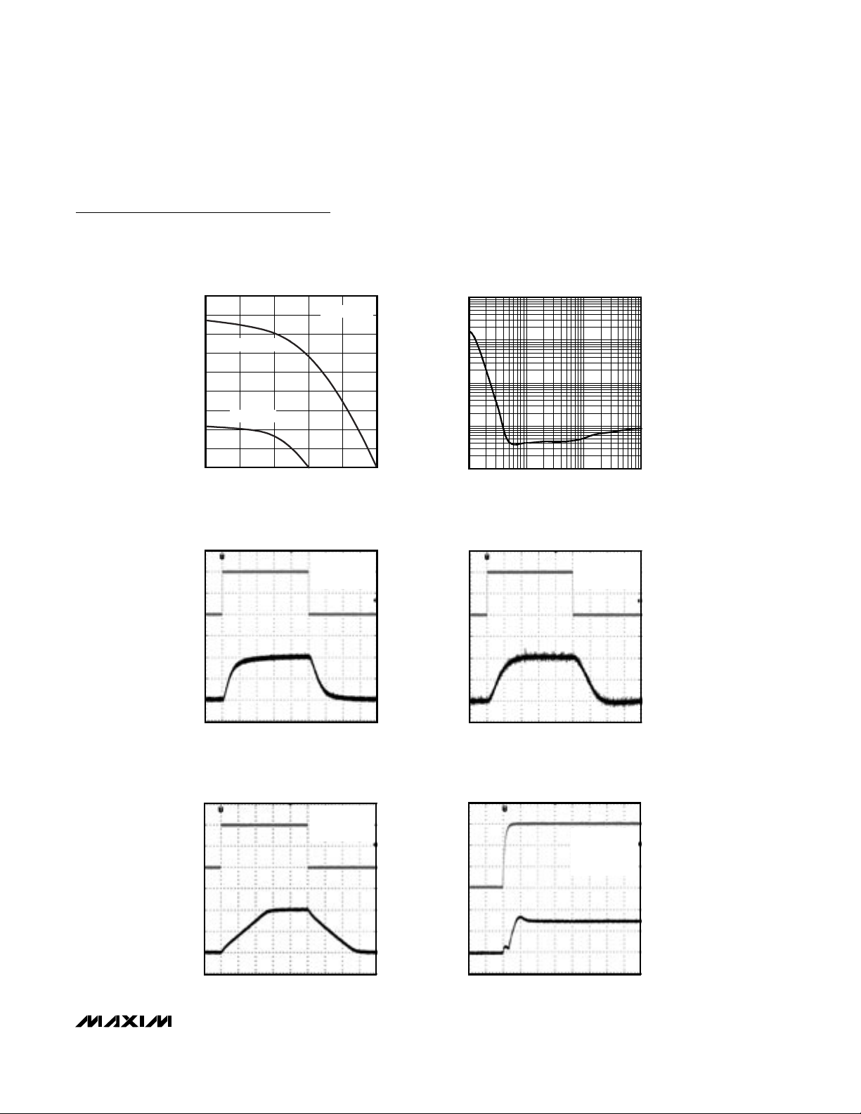
MAX4036–MAX4039
Low I
BIAS
, +1.4V/800nA, Rail-to-Rail Op Amps
with +1.2V Buffered Reference
________________________________________________________________________________________ 7
OP AMP SOURCE CURRENT
vs. OUTPUT VOLTAGE
MAX4036 toc19
V
OUT_
(V)
SOURCE CURRENT (mA)
2.41.81.20.6
2
4
6
8
10
12
14
16
18
0
03.0
VDD = 3.0V
VDD = 1.8V
VID = +100mV
1000
0.1
10 1k 10k
OP AMP VOLTAGE NOISE DENSITY
vs. FREQUENCY
1
10
100
MAX4036 toc20
FREQUENCY (Hz)
NOISE (µV/√Hz)
100
OP AMP
SMALL-SIGNAL TRANSIENT RESPONSE
MAX4036 toc21
2.55V
2.45V
2.55V
2.45V
V
IN
+
V
OUT_
AV = 1V/V
C
L
= 12pF TO V
SS
RL = 1MΩ TO V
SS
OP AMP
SMALL-SIGNAL TRANSIENT RESPONSE
MAX4036 toc22
40µs/div
AV = 1V/V
C
L
= 250pF TO V
SS
RL = 1MΩ TO V
SS
VIN+
V
OUT_
2.55V
2.45V
2.55V
2.45V
OP AMP
LARGE-SIGNAL TRANSIENT RESPONSE
MAX4036 toc23
100µs/div
AV = 1V/V
C
L
= 12pF TO V
SS
RL = 1MΩ TO V
SS
VIN+
V
OUT_
500mV/div
2.5V
1.5V
OP AMP
TURN-ON TRANSIENT RESPONSE
MAX4036 toc24
100µs/div
3.0V
0V
V
OUT_
50mV/div
AV = 1V/V
C
L
= 12pF TO GND
R
L
= 1MΩ TO GND
V
IN
+ = VDD / 2
V
DD
Typical Operating Characteristics (continued)
(VDD= 3V, VSS= VCM= 0V, RLto VDD/2, TA= +25°C, unless otherwise noted.)
Page 8
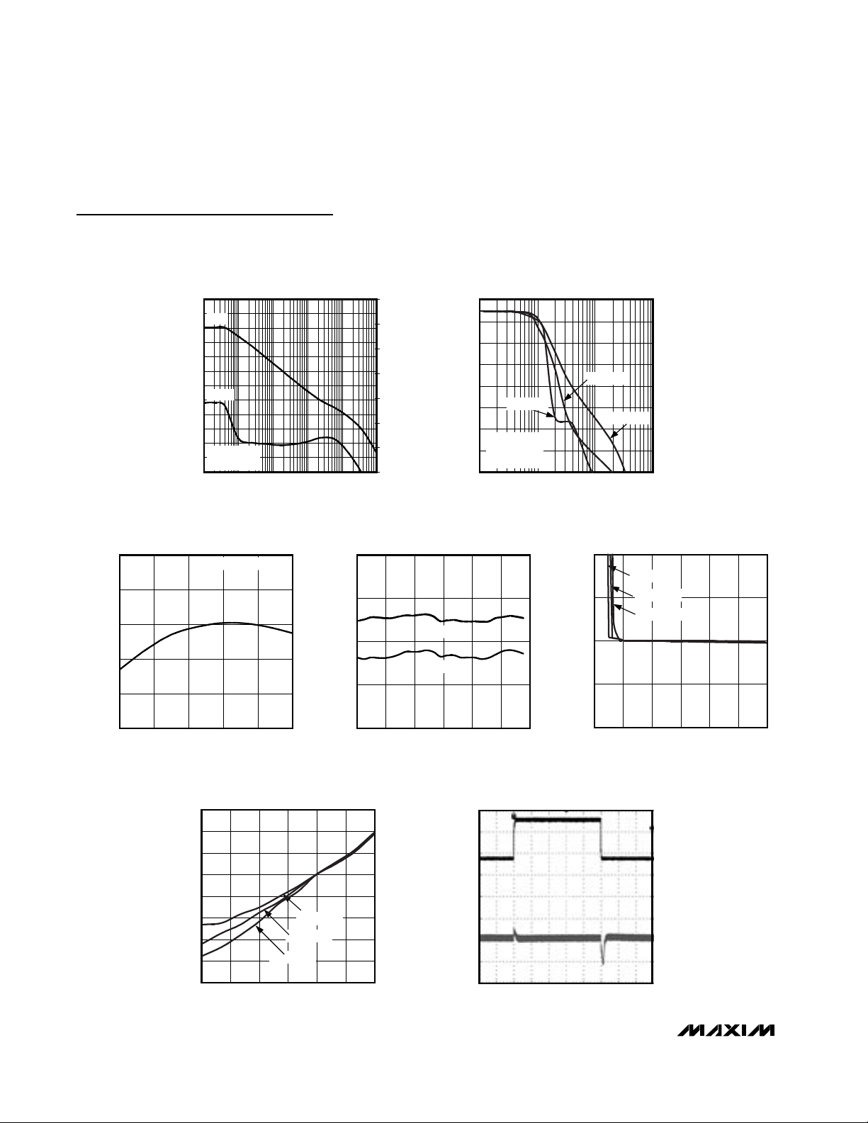
MAX4036–MAX4039
Low I
BIAS
, +1.4V/800nA, Rail-to-Rail Op Amps
with +1.2V Buffered Reference
8 _______________________________________________________________________________________
80
70
60
50
40
30
20
10
0
-10
-20
-30
-40
110100 1k 10k 100k
GAIN AND PHASE
vs. FREQUENCY
MAX4036 toc25
FREQUENCY (Hz)
GAIN (dB)
180
135
90
45
0
-45
-90
-135
PHASE (DEGREES)
AV = 1000V/V
V
IN_
= 1mV
P-P
GAIN
PHASE
2
-30
100 10k 100k
LARGE-SIGNAL GAIN
vs. FREQUENCY
-22
-26
-18
-14
-10
-6
-2
MAX4036 toc26
FREQUENCY (Hz)
GAIN (dB)
1k
RL = 1MΩ
AV = 1
V
OUT_
= 1V
P-P
CL = 12pF
RL = 100kΩ
RL = 5kΩ
REFERENCE VOLTAGE
vs. TEMPERATURE
MAX4036 toc27
TEMPERATURE (°C)
V
REF
(V)
603510-15
1.228
1.230
1.232
1.234
1.236
1.226
-40 85
MAX4037/MAX4039
REFERENCE VOLTAGE CHANGE
vs. TIME
MAX4036 toc28
TIME (HR)
V
REF
(V)
500400300200100
1.231
1.232
1.233
1.234
1.230
0600
MAX4037
MAX4039
REFERENCE VOLTAGE CHANGE
vs. LOAD CURRENT
MAX4036 toc29
LOAD CURRENT (µA)
NORMALIZED V
REF
4003002001000
0.99
1.00
1.01
1.02
0.98
-100 500
TA = +85°C
TA = +25°C
TA = -40°C
REFERENCE VOLTAGE CHANGE
vs. SUPPLY VOLTAGE
MAX4036 toc30
VDD (V)
NORMALIZED V
REF
3.33.02.1 2.4 2.7
0.9996
0.9997
0.9998
0.9999
1.0000
1.0001
1.0002
1.0003
0.9995
1.8 3.6
TA = +85°C
TA = +25°C
TA = -40°C
Typical Operating Characteristics (continued)
(VDD= 3V, VSS= VCM= 0V, RLto VDD/2, TA= +25°C, unless otherwise noted.)
REFERENCE LINE-TRANSIENT RESPONSE
MAX4036 toc31
1ms/div
V
DD
V
REF
AC-COUPLED
50mV/div
0V
1.8V
3.6V
Page 9

MAX4036–MAX4039
Low I
BIAS
, +1.4V/800nA, Rail-to-Rail Op Amps
with +1.2V Buffered Reference
_______________________________________________________________________________________ 9
REFERENCE LOAD-TRANSIENT RESPONSE
(SINKING CURRENT)
MAX4036 toc32
2.5ms/div
0
V
REF
500mV/div
0
2µA
I
REF
MAX4036 toc33
2.5ms/div
0
0
20µA
I
REF
V
REF
500mV/div
REFERENCE LOAD-TRANSIENT RESPONSE
(SINKING CURRENT)
REFERENCE LOAD-TRANSIENT RESPONSE
(SOURCING CURRENT)
MAX4036 toc34
1ms/div
0
0
I
REF
10µA
V
REF
500mV/div
MAX4036 toc35
1ms/div
0
0
I
REF
100µA
V
REF
500mV/div
REFERENCE LOAD-TRANSIENT RESPONSE
(SOURCING CURRENT)
REFERENCE TURN-ON
TRANSIENT RESPONSE
MAX4036 toc36
1ms/div
V
DD
0V
3V
0V
V
REF
0.1Hz TO 10Hz REFERENCE NOISE
MAX4036 toc37
1s/div
20µV/div
Typical Operating Characteristics (continued)
(VDD= 3V, VSS= VCM= 0V, RLto VDD/2, TA= +25°C, unless otherwise noted.)
Page 10

MAX4036–MAX4039
Low I
BIAS
, +1.4V/800nA, Rail-to-Rail Op Amps
with +1.2V Buffered Reference
10 ______________________________________________________________________________________
Detailed Description
The MAX4036–MAX4039 consume an ultra-low supply
current and have rail-to-rail output stages specifically
designed for low-voltage operation. The input commonmode voltage range extends from V
DD
- 0.4V to VSS,
although full rail-to-rail input range is possible with
degraded performance when operating from a supply
voltage above 3.0V. The input offset voltage is typically
200µV. Low-operating supply voltage, low supply current,
and rail-to-rail outputs make the MAX4036–MAX4039 an
excellent choice for precision or general-purpose lowvoltage, battery-powered systems.
Rail-to-Rail Outputs
The MAX4036–MAX4039 output stages can drive a 5kΩ
load and still swing to within 40mV of the rails. Figure 1
shows the output voltage swing of the MAX4036–
MAX4039 configured as a unity-gain buffer, powered
from a single 2.4V supply. The output for this setup typically swings from 5mV to VDD- 5mV with a 100kΩ load.
Pin Description
PIN
MAX4036
NAME FUNCTION
13——IN+ Noninverting Amplifier Input
2 245VSSNegative Power-Supply Voltage
34——IN- Inverting Amplifier Input
41——OUT Amplifier Output
56810VDDPositive Power-Supply Voltage
—5—6REF Reference Voltage Output
—— 11OUTA Amplifier Output (Channel A)
—— 22INA- Inverting Amplifier Input (Channel A)
—— 33INA+ Noninverting Amplifier Input (Channel A)
—— 57INB+ Noninverting Amplifier Input (Channel B)
—— 68INB- Inverting Amplifier Input (Channel B)
—— 79OUTB Amplifier Output (Channel B)
———4N.C. No Connection. Not internally connected.
— ———
EP
Exposed Paddle. Solder EP to VSS or leave unconnected
(TDFN packages only).
Figure 1. Rail-to-Rail Input/Output Voltage Range
MAX4037 MAX4038 MAX4039
(TDFN only)
V
V
OUT+
IN_+
AV = 1V/V
1.5V
1.5V
2ms/div
1V/div
Page 11
MAX4036–MAX4039
Low I
BIAS
, +1.4V/800nA, Rail-to-Rail Op Amps
with +1.2V Buffered Reference
______________________________________________________________________________________ 11
Applications Information
Power-Supply Considerations
The MAX4036–MAX4039 operate from a single 1.4V
(MAX4036/MAX4038) or 1.8V (MAX4037/MAX4039) to
3.6V supply. A high amplifier power-supply rejection
ratio of 82dB and the excellent reference line regulation
allow the devices to be powered directly from a decaying battery voltage, simplifying design and extending
battery life. The MAX4036–MAX4039 are ideally suited
for low-voltage battery-powered systems. The Typical
Operating Characteristics show the changes in supply
current and reference output as a function of supply
voltage.
Power-Up Settling Time
The MAX4036–MAX4039 typically require 0.25ms to
power-up. During this startup time, the output is indeterminate. The application circuit should allow for this
initial delay. See the Typical Operating Characteristics
for amplifier and reference settling time curves.
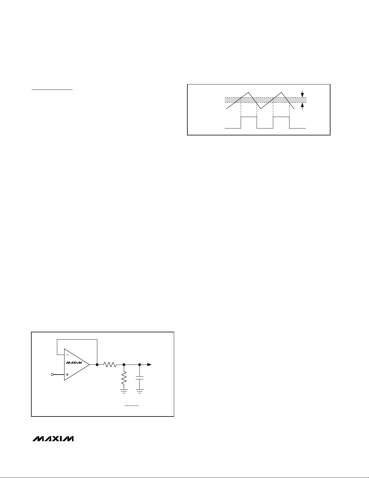
Driving Capacitive Loads: Op Amps
The MAX4036–MAX4039 amplifier(s) require no output
capacitor for stability, and are unity-gain stable for
loads up to 5000pF. Applications that require greater
capacitive-drive capability should use an isolation
resistor between the output and the capacitive load
(Figure 2). Note that this solution reduces the gain and
output voltage swing because R
ISO
forms a voltage-
divider with the load resistor.
Crossover Distortion
The MAX4036–MAX4039 output stages are capable of
sourcing and sinking currents with orders of magnitude
greater than the stages’ quiescent current, which is
less than 1µA. This ability to drive heavy loads with
such a small quiescent current introduces crossover
distortion as the output stage passes between sinking
and sourcing. In the crossover regions, the output
impedance of the MAX4036–MAX4039 increases substantially, thereby changing the load-driving characteristics. The distortion can be greatly reduced by
increasing the load resistance. For applications where
low load resistance is required, bias the load such that
the output current is always in one direction, to avoid
crossover distortion.
Reference Bypassing
The MAX4037/MAX4039 reference requires no external
capacitors.
Using the MAX4036–MAX4039 as a
Comparator
Although optimized for use as an operational amplifier,
the MAX4036–MAX4039 can be used as a rail-to-rail
I/O comparator (Figures 3, 4). External hysteresis can
be used to minimize the risk of output oscillation. The
positive feedback circuit, shown in Figure 4, causes the
input threshold to change when the output voltage
changes state.
Battery Monitoring Using the
MAX4037/MAX4039 and Hysteresis
The internal reference and low operating voltage of the
MAX4037/MAX4039 make the devices ideal for batterymonitoring applications. Hysteresis can be set using
resistors as shown in Figure 4, and the following design
procedure:
1) Choose R3. The input bias current of IN_+ is under
100pA over temperature, so a current through R3
around 100nA maintains accuracy. The current
through R3 at the trip point is V
REF
/ R3, or 100nA
for R3 = 12MΩ. 10MΩ is a good practical value.
2) Choose the hysteresis voltage (VHB), the voltage
between the upper and lower thresholds. In this
example, choose VHB= 50mV (see Figure 3).
MAX4038
R
ISO
R
L
C
L
R
L
RL + R
ISO
AV = = 1
Figure 2. Using a Resistor to Isolate a Capacitive Load from
the Op Amp
V
HB
V
OH
V
OL
V
THR
V
THF
INPUT
OUTPUT
Figure 3. Hysteresis
Page 12

MAX4036–MAX4039
Low I
BIAS
, +1.4V/800nA, Rail-to-Rail Op Amps
with +1.2V Buffered Reference
12 ______________________________________________________________________________________
3) Calculate R1:
4) Choose the threshold voltage for V
IN
rising (V
THR
).
In this example, choose V
THR
= 2.0V.
5) Calculate R2:
6) Verify the threshold voltages with these formulas:
VINrising:
VINfalling:
In this application, the MAX4036–MAX4039 supply current will vary, depending on the output state of the
comparator.
Power Supplies and Layout
The MAX4036–MAX4039 operate from a single 1.4V
(MAX4036/MAX4038) or 1.8V (MAX4037/MAX4039) to
3.6V power supply. Bypass VDDwith a 0.1µF capacitor
to ground to minimize noise.
Good layout techniques optimize performance by
decreasing the amount of stray capacitance to the op
amp’s inputs and outputs. To decrease stray capacitance, minimize trace lengths by placing external components close to the device.
The exposed paddle (EP) on the TDFN packages of the
MAX4038 and MAX4039 is internally connected to the
device substrate, V
SS
. Connect the exposed paddle to
VSSor leave EP unconnected. Running traces below the
exposed paddle is not recommended.
Chip Information
MAX4036 TRANSISTOR COUNT: 49
MAX4037 TRANSISTOR COUNT: 119
MAX4038 TRANSISTOR COUNT: 146
MAX4039 TRANSISTOR COUNT: 146
PROCESS: BiCMOS
VV
RV
R
THF THR
DD
= −
×
1
3
VVR
RR R
THR REF
=××++
1
1
1
1
2
1
3
R
V
VRRR
V
Vk k M
k
THR
REF
2
1
1
1
1
1
3
1
20
12 210
1
210
1
10
325
.
.
=
×
−−
=
×
−−
=
ΩΩΩ
Ω
RR
V
V
M
V
V
k
HB
DD
13
10
05
24
210
.
.
=×
=×
=
Ω
Ω
V
REF
R3
R1
R2
V
BATT
V
BGOOD
V
SS
V
SS
V
DD
V
DD
IN+
REF
IN-
OUT
MAX4037
Figure 4. Battery Monitoring
Selector Guide
PART
REFERENCE
MAX4036 1 —
MAX4037 1 √
MAX4038 2 —
MAX4039 2 √
NO. OF AMPLIFIERS
Page 13

MAX4036–MAX4039
Low I
BIAS
, +1.4V/800nA, Rail-to-Rail Op Amps
with +1.2V Buffered Reference
______________________________________________________________________________________ 13
Pin Configurations
INB-
OUTB
INB+V
SS
1
2
8
7
V
DD
INA-
INA+
OUTA
µMAX
3
4
6
5
1
2
3
4
5
10
9
8
7
6
V
DD
OUTB
INB-
INB+N.C.
INA+
INA-
OUTA
µMAX
REF
V
SS
TDFN EXPOSED PAD CONNECTED TO VSS.
OUT
IN+
1
2
3
6
4
IN-
V
SS
V
SS
V
SS
V
DD
V
DD
V
DD
SOT23
5
REF
IN+
IN-
1
2
3
5
4
OUT
V
SS
V
DD
SC70
TOP VIEW
OUTA
INA-
INA+
N.C.
OUTB
INB-
INB+
REF
3mm x 3mm x 0.8mm TDFN
OUTA
INA-
INA+
1
2
3
4
1
2
3
4
5
OUTB
INB-
INB+
8
7
6
5
8
7
6
9
10
3mm x 3mm x 0.8mm TDFN
MAX4036 MAX4037
MAX4038
MAX4038
MAX4039
MAX4039
Page 14

MAX4036–MAX4039
Low I
BIAS
, +1.4V/800nA, Rail-to-Rail Op Amps
with +1.2V Buffered Reference
14 ______________________________________________________________________________________
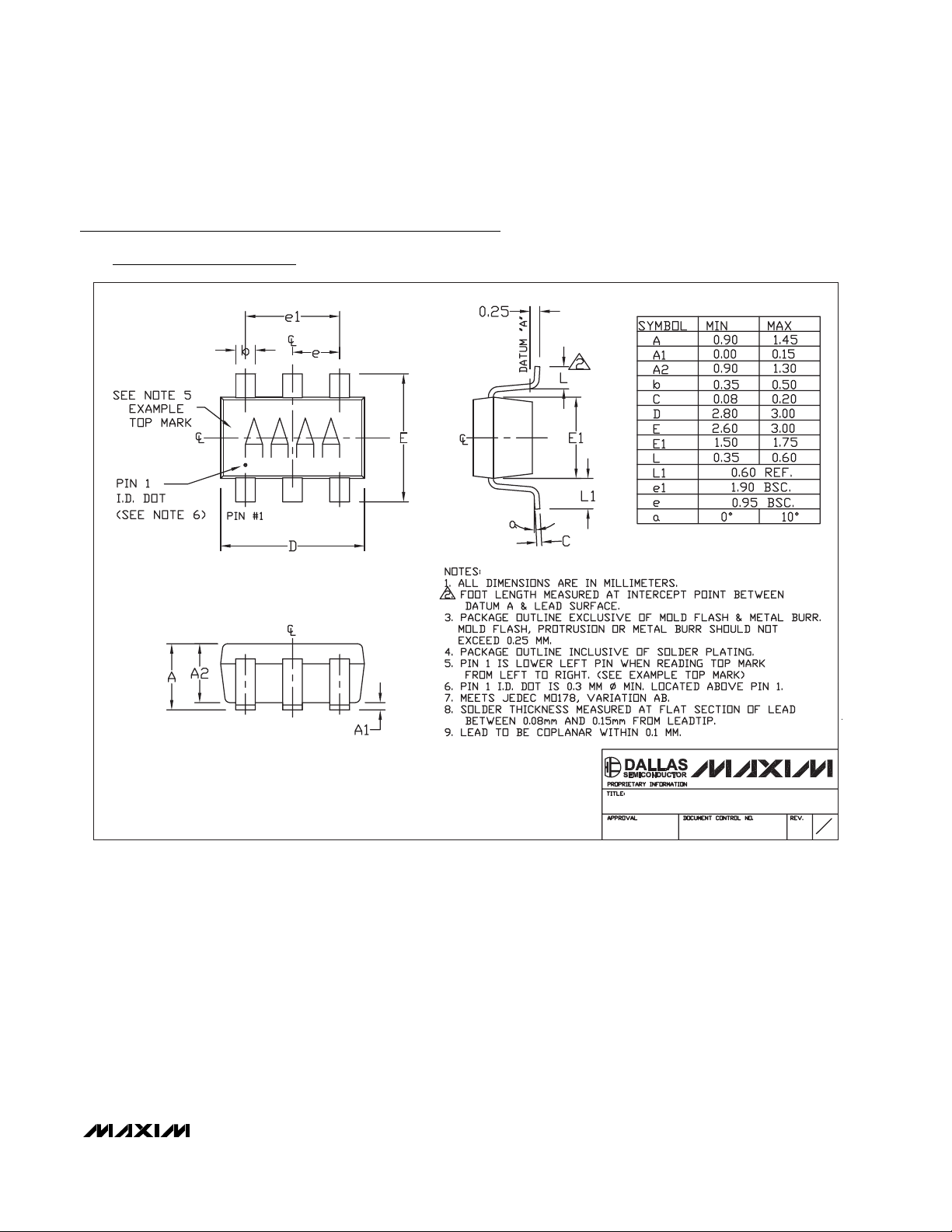
SC70 5L EPS
Package Information
(The package drawing(s) in this data sheet may not reflect the most current specifications. For the latest package outline information,
go to www.maxim-ic.com/packages
.)
Page 15
MAX4036–MAX4039
Low I
BIAS
, +1.4V/800nA, Rail-to-Rail Op Amps
with +1.2V Buffered Reference
______________________________________________________________________________________ 15
6LSOT.EPS
F
1
1
21-0058
PACKAGE OUTLINE, SOT-23, 6L
Package Information (continued)
(The package drawing(s) in this data sheet may not reflect the most current specifications. For the latest package outline information,
go to www.maxim-ic.com/packages
.)
Page 16

MAX4036–MAX4039
Low I
BIAS
, +1.4V/800nA, Rail-to-Rail Op Amps
with +1.2V Buffered Reference
16 ______________________________________________________________________________________
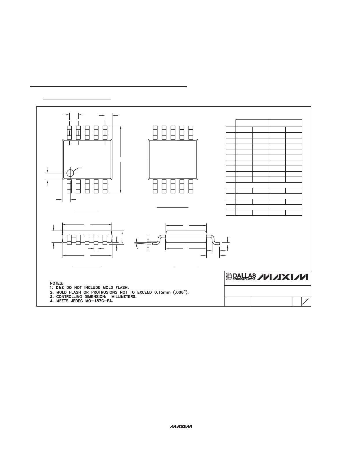
8LUMAXD.EPS
PACKAGE OUTLINE, 8L uMAX/uSOP
1
1
21-0036
J
REV.DOCUMENT CONTROL NO.APPROVAL
PROPRIETARY INFORMATION
TITLE:
MAX
0.043
0.006
0.014
0.120
0.120
0.198
0.026
0.007
0.037
0.0207 BSC
0.0256 BSC
A2
A1
c
e
b
A
L
FRONT VIEW
SIDE VIEW
E H
0.6±0.1
0.6±0.1
ÿ 0.50±0.1
1
TOP VIEW
D
8
A2
0.030
BOTTOM VIEW
1
6∞
S
b
L
H
E
D
e
c
0∞
0.010
0.116
0.116
0.188
0.016
0.005
8
4X S
INCHES
-
A1
A
MIN
0.002
0.950.75
0.5250 BSC
0.25 0.36
2.95 3.05
2.95 3.05
4.78
0.41
0.65 BSC
5.03
0.66
6∞0∞
0.13 0.18
MAX
MIN
MILLIMETERS
- 1.10
0.05 0.15
α
α
DIM
Package Information (continued)
(The package drawing(s) in this data sheet may not reflect the most current specifications. For the latest package outline information,
go to www.maxim-ic.com/packages
.)
Page 17

MAX4036–MAX4039
Low I
BIAS
, +1.4V/800nA, Rail-to-Rail Op Amps
with +1.2V Buffered Reference
______________________________________________________________________________________ 17
6, 8, &10L, DFN THIN.EPS
PROPRIETARY INFORMATION
TITLE:
APPROVAL
DOCUMENT CONTROL NO. REV.
2
1
PACKAGE OUTLINE, 6, 8 & 10L,
TDFN, EXPOSED PAD, 3x3x0.80 mm
21-0137 D
L
C
L
C
SEMICONDUCTOR
DALLAS
A2
A
PIN 1
INDEX
AREA
D
E
A1
D2
b
E2
[(N/2)-1] x e
REF.
e
k
1N1
L
e
L
A
L
PIN 1 ID
C0.35
DETAIL A
e
NUMBER OF LEADS SHOWN ARE FOR REFERENCE ONLY
DOCUMENT CONTROL NO.APPROVAL
TITLE:
PROPRIETARY INFORMATION
REV.
2
2
COMMON DIMENSIONS
SYMBOL
MIN. MAX.
A
0.70 0.80
D
2.90 3.10
E
2.90 3.10
A1
0.00 0.05
L
0.20 0.40
PKG. CODE
6
N
T633-1 1.50±0.10D22.30±0.10
E2
0.95 BSCeMO229 / WEEA
JEDEC SPEC
0.40±0.05b1.90 REF
[(N/2)-1] x e
1.50±0.10
MO229 / WEEC
1.95 REF0.30±0.05
0.65 BSC
2.30±0.10T833-1 8
PACKAGE VARIATIONS
21-0137
0.25±0.05 2.00 REFMO229 / WEED-30.50 BSC1.50±0.10 2.30±0.1010T1033-1
0.25 MIN.
k
A2 0.20 REF.
D
SEMICONDUCTOR
DALLAS
PACKAGE OUTLINE, 6, 8 & 10L,
TDFN, EXPOSED PAD, 3x3x0.80 mm
Package Information (continued)
(The package drawing(s) in this data sheet may not reflect the most current specifications. For the latest package outline information,
go to www.maxim-ic.com/packages
.)
Page 18
10LUMAX.EPS
PACKAGE OUTLINE, 10L uMAX/uSOP
1
1
21-0061
I
REV.DOCUMENT CONTROL NO.APPROVAL
PROPRIETARY INFORMATION
TITLE:
TOP VIEW
FRONT VIEW
1
0.498 REF
0.0196 REF
S
6∞
SIDE VIEW
α
BOTTOM VIEW
0∞ 0∞ 6∞
0.037 REF
0.0078
MAX
0.006
0.043
0.118
0.120
0.199
0.0275
0.118
0.0106
0.120
0.0197 BSC
INCHES
1
10
L1
0.0035
0.007
e
c
b
0.187
0.0157
0.114
H
L
E2
DIM
0.116
0.114
0.116
0.002
D2
E1
A1
D1
MIN
-A
0.940 REF
0.500 BSC
0.090
0.177
4.75
2.89
0.40
0.200
0.270
5.05
0.70
3.00
MILLIMETERS
0.05
2.89
2.95
2.95
-
MIN
3.00
3.05
0.15
3.05
MAX
1.10
10
0.6±0.1
0.6±0.1
ÿ 0.50±0.1
H
4X S
e
D2
D1
b
A2
A
E2
E1
L
L1
c
α
GAGE PLANE
A2 0.030 0.037 0.75 0.95
A1
Package Information (continued)
(The package drawing(s) in this data sheet may not reflect the most current specifications. For the latest package outline information,
go to www.maxim-ic.com/packages
.)
MAX4036–MAX4039
Low I
BIAS
, +1.4V/800nA, Rail-to-Rail Op Amps
with +1.2V Buffered Reference
Maxim cannot assume responsibility for use of any circuitry other than circuitry entirely embodied in a Maxim product. No circuit patent licenses are
implied. Maxim reserves the right to change the circuitry and specifications without notice at any time.
18 ____________________Maxim Integrated Products, 120 San Gabriel Drive, Sunnyvale, CA 94086 408-737-7600
© 2004 Maxim Integrated Products Printed USA is a registered trademark of Maxim Integrated Products.
 Loading...