

Page 1
General Description
The MAX3983 is a quad copper-cable signal conditioner
that operates from 2.5Gbps to 3.2Gbps. It provides compensation for 4x copper InfiniBand and 10Gbase-CX4
Ethernet links, allowing spans of 20m with 24AWG and
15m with 28AWG. The cable driver section provides four
selectable preemphasis levels. The input to the cable
driver compensates for up to 0.5m of FR4 circuit board
material. The cable receiver section provides additional
fixed input equalization while offering selectable preemphasis to drive FR4 circuit boards up to 0.5m.
The MAX3983 also features signal detection on all eight
inputs and internal loopback that allows for diagnostic
testing. It is packaged in a 10mm x 10mm, 68-pin QFN
and operates from 0°C to +85°C.
Applications
4x InfiniBand (4 x 2.5Gbps)
10Gbase-CX4 Ethernet (4 x 3.125Gbps)
10G Fibre Channel XAUI (4 x 3.1875Gbps)
4x Copper-Cable or Backplane Transmission
(1Gbps to 3.2Gbps)
Features
♦ Link Features
Span 20m with 24AWG, 15m with 28AWG
Span 0.5m of FR4 on Each Host
1.6W Total Power with 3.3V Supply
Loopback Function
♦ Cable Driver Features
Selectable Output Preemphasis
FR4 Input Equalization
Signal Detect for Each Channel
Output Disable
♦ Cable Receiver Features
Selectable FR4 Output Preemphasis
Cable Input Equalization
Signal Detect for Each Channel
Output Disable
MAX3983
Quad Copper-Cable Signal Conditioner
________________________________________________________________ Maxim Integrated Products 1
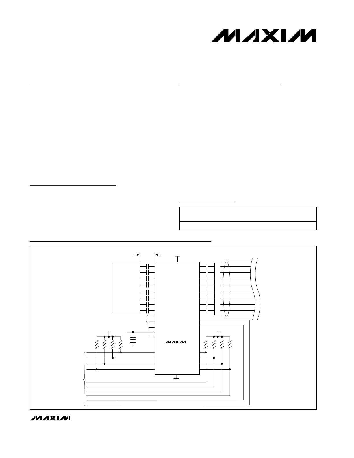
Typical Application Circuit
Ordering Information
19-2928; Rev 0; 7/03
For pricing, delivery, and ordering information, please contact Maxim/Dallas Direct! at
1-888-629-4642, or visit Maxim’s website at www.maxim-ic.com.
Pin Configuration appears at end of data sheet.
≤0.5m
0.01µF 0.01µF
TX_IN1
GND
TX_IN2
TX_IN3
TX_IN4
RX_OUT1
RX_OUT2
RX_OUT3
RX_OUT4
TX_PE0
OR
TX_PE1
RX_PE
POR
LOOPBACK
RX_SD1
RX_SD2
RX_SD3
RX_SD4
TX
SERDES
RX
V
CC
3V TO 5.5V
TO HOST
C
4.7kΩ 4.7kΩ
TO HOST
POR
PART TEMP RANGE
MAX3983UGK 0°C to +85°C 68 QFN G6800-4
3.3V
[1:4]
V
CC
MAX3983
GND
TX_OUT1
TX_OUT2
TX_OUT3
TX_OUT4
RX_IN1
RX_IN2
RX_IN3
RX_IN4
TX_ENABLE
RX_ENABLE
TX_SD1
TX_SD2
TX_SD3
TX_SD4
4x COPPER CABLE ASSEMBLY
≤20m (24AWG)
≤15m (28AWG)
3V TO 5.5V
PINPACKAGE
TO MAX3983
PKG CODE
Page 2
MAX3983
Quad Copper-Cable Signal Conditioner
2 _______________________________________________________________________________________
ABSOLUTE MAXIMUM RATINGS
ELECTRICAL CHARACTERISTICS
(VCC= +3.0V to +3.6V, TA= 0°C to +85°C. Typical values are at VCC= +3.3V and TA= +25°C, unless otherwise noted.)
Stresses beyond those listed under “Absolute Maximum Ratings” may cause permanent damage to the device. These are stress ratings only, and functional
operation of the device at these or any other conditions beyond those indicated in the operational sections of the specifications is not implied. Exposure to
absolute maximum rating conditions for extended periods may affect device reliability.
Supply Voltage, VCC..............................................-0.5V to +6.0V
Continuous CML Output Current at
TX_OUT[1:4]±, RX_OUT[1:4]± ..........................……….±25mA
Voltage at TX_IN[1:4]±, RX_IN[1:4]±, RX_SD[1:4],
TX_SD[1:4], RX_ENABLE, TX_ENABLE, RX_PE,
TX_PE[0:1], LOOPBACK, POR
(with series resistor ≥4.7kΩ)...................-0.5V to (V
CC
+ 0.5V)
Continuous Power Dissipation (T
A
= +85°C)
68-Pin QFN (derate 41.7mW/°C above +85°C)………….2.7W
Operating Junction Temperature Range (T
J
) ....-55°C to +150°C
Storage Ambient Temperature Range (T
S
) .......-55°C to +150°C
Supply Current
OPERATING CONDITIONS
Supply Voltage V
Supply Noise Tolerance 1MHz ≤ f < 2GHz 40 mV
Operating Ambient Temperature T
Bit Rate NRZ data (Note 1) 2.5 3.2 Gbps
CID Consecutive identical digits (bits) 10 Bits
STATUS OUTPUTS: RX_SD[1:4], TX_SD[1:4]
Signal-Detect Open-Collector
Current Sink
Signal-Detect Response Time
Signal-Detect Transition Time Rise time or fall time (10% to 90%) 200 ns
Power-On Reset Delay 1µF capacitor on POR to GND 6 ms
CONTROL INPUTS: RX_ENABLE, TX_ENABLE, RX_PE, TX_PE0, TX_PE1, LOOPBACK
Voltage, Logic High V
Voltage, Logic Low V
Current, Logic High I
Current, Logic Low I
PARAMETER SYMBOL CONDITIONS MIN TYP MAX UNITS
RX_EN = VCC, TX_EN = 0V 360 430
RX_EN = 0V, TX_EN = V
RX_EN = V
CC
A
Signal detect asserted 0 25 µA
Signal detect unasserted VOL ≤ 0.4V with 4.7kΩ
pullup resistor
= 0V, pullup supply = 5.5V, external pullup
V
CC
resistor ≥4.7kΩ
Time from RX_IN[1:4] or TX_IN[1:4] dropping
below 85mV
50% point of signal detect
IH
IL
VIH = V
IH
VIL = 0V -150 +150 µA
IL
, TX_EN = V
CC
or rising above 175mV
P-P
CC
CC
CC
P-P
to
365 430
495 580
3.0 3.3 3.6 V
02585°C
1.0 1.11 mA
025µA
0.35 µs
1.5 V
0.5 V
-150 +150 µA
mA
P-P
Page 3
MAX3983
Quad Copper-Cable Signal Conditioner
_______________________________________________________________________________________ 3
ELECTRICAL CHARACTERISTICS (continued)
(VCC= +3.0V to +3.6V, TA= 0°C to +85°C. Typical values are at VCC= +3.3V and TA= +25°C, unless otherwise noted.)
TX SECTION (CABLE DRIVER)
PC Board Input Swing
Input Resistance TX_IN[1:4]+ to TX_IN[1:4]-, differential 85 100 115 Ω
Input Return Loss 100MHz to 2GHz (Note 1) 10 17 dB
Output Swing
Output Resistance
Output Return Loss 100MHz to 2GHz (Note 1) 10 13 dB
Output Transition Time tr, tf20% to 80% (Notes 1, 3) 80 ps
Random Jitter (Notes 1, 3) 1.6 ps
Output Preemphasis See Figure 1
Residual Output Deterministic
Jitter at 2.5Gbps (Notes 1, 4, 5)
Residual Output Deterministic
Jitter at 3.2Gbps (Notes 1, 4, 5)
Signal-Detect Assert Level TX_IN for TX_SD = high (Note 6) 800 mV
Signal-Detect Off TX_IN for TX_SD = low (Note 6) 200 mV
RX SECTION (CABLE RECEIVER)
Cable Input Swing
Input Vertical Eye Opening
Input Resistance RX_IN[1:4]+ to RX_IN[1:4]-, differential 85 100 115 Ω
Input Return Loss 100MHz to 2GHz (Note 1) 10 18 dB
PARAMETER SYMBOL CONDITIONS MIN TYP MAX UNITS
Measured differentially at the signal source
(Note 1)
TX_ENABLE = high (Notes 1, 2) 1300 1500 1600
TX_ENABLE = low 30
TX_OUT[1:4]+ or TX_OUT[1:4]- to V
ended
TX_PE1 TX_PE0
00 3
01 6
10 9
11 12
Source to
TX_IN
6-mil FR4 ≤
20in
Source to
TX_IN
6-mil FR4 ≤
20in
Measured differentially at the signal source
(Note 1)
Measured differentially at the input of the
MAX3983 (Note 1)
TX_OUT to
Load
1m, 28AWG 0 0
5m, 28AWG 0 1
10m, 24AWG 1 0
15m, 24AWG 1 1
TX_OUT to
Load
1m, 28AWG 0 0
5m, 28AWG 0 1
10m, 24AWG 1 0
15m, 24AWG 1 1
, single
CC
TX_PE1 TX_PE0
TX_PE1 TX_PE0
800 1600 mV
mV
42 50 58 Ω
0.10 0.15 UI
0.15 0.20 UI
1000 1600 mV
175 1600 mV
P-P
P-P
RMS
dB
P-P
P-P
P-P
P-P
P-P
P-P
Page 4

MAX3983
Quad Copper-Cable Signal Conditioner
4 _______________________________________________________________________________________
ELECTRICAL CHARACTERISTICS (continued)
(VCC= +3.0V to +3.6V, TA= 0°C to +85°C. Typical values are at VCC= +3.3V and TA= +25°C, unless otherwise noted.)
Output Swing
Output Resistance
Output Return Loss 100MHz to 2GHz (Note 1) 10 15 dB
Output Transition Time tr, tf20% to 80% (Notes 1, 8) 45 80 ps
Random Jitter (Notes 1, 8) 1.6 ps
Output Preemphasis
Residual Output Deterministic
Jitter at 2.5Gbps
(Notes 1, 5, 9, 10)
PARAMETER SYMBOL CONDITIONS MIN TYP MAX UNITS
RX_ENABLE = high (Notes 1, 7) 1100 1500
RX_ENABLE = low 30
RX_OUT[1:4]+ or RX_OUT[1:4]- to V
ended
RX_PE = low 3
RX_PE = high 6
Source to
RX_IN
5m, 28AWG
IB Cable
Assembly
without
preemphasis
RX_OUT to
Load
0in, 6-mil FR4 0
20in, 6-mil FR4 1
, single
CC
RX_PE
42 50 58 Ω
0.10 0.15 UI
mV
P-P
RMS
dB
P-P
Source to
RX_IN
Residual Output Deterministic
Jitter at 3.2Gbps
(Notes 1, 5, 9, 10)
Signal-Detect Assert Level RX_IN for RX_SD = high (Note 11) 175 mV
Signal-Detect Off RX_IN for RX_SD = low (Note 11) 85 mV
END-TO-END JITTER (TX AND RX COMBINED PERFORMANCE)
Residual Output Deterministic
Jitter at 2.5Gbps
(Notes 1, 12, 13, 14)
5m, 28AWG
IB cable
assembly
without
preemphasis
Source to
TX_IN
6-mil FR4 ≤
20in
RX_OUT to
Load
0in, 6-mil FR4 0
20in, 6-mil FR4 1
TX_OUT to
RX_IN
1m, 24AWG 0 0 0in 0
15m, 24AWG 1 1 20in 1
20m, 24AWG 1 1 20in 1 0.2 0.25
RX_PE
TX_PE1
TX_PE0
RX_OUT to Load
RX_PE
0.15 0.20 UI
0.15 0.20
UI
P-P
P-P
P-P
P-P
Page 5
MAX3983
Quad Copper-Cable Signal Conditioner
_______________________________________________________________________________________ 5
ELECTRICAL CHARACTERISTICS (continued)
(VCC= +3.0V to +3.6V, TA= 0°C to +85°C. Typical values are at VCC= +3.3V and TA= +25°C, unless otherwise noted.)
Note 1: Guaranteed by design and characterization.
Note 2: Measured with 2in of FR4 through InfiniBand connector with TX_PE1 = TX_PE0 =1.
Note 3: Measured at the chip using 0000011111 or equivalent pattern. TX_PE1 = TX_PE0 = 0 for minimum preemphasis.
Note 4: All channels under test are not transmitting during test. Channel tested with XAUI CJPAT, as well as this pattern: 19 zeros,
1, 10 zeros, 1010101010 (D21.5 character), 1100000101 (K28.5+ character), 19 ones, 0, 10 ones, 0101010101 (D10.2
character), 0011111010 (K28.5- character).
Note 5: Cables are unequalized, Amphenol Spectra-Strip 24AWG and 28AWG or equivalent equipped with Fujitsu “MicroGiga”
connector or equivalent. All other channels are quiet. Residual deterministic jitter is the difference between the source jitter and the output jitter at the load. The deterministic jitter (DJ) at the output of the transmission line must be from mediainduced loss and not from clock-source modulation. Depending upon the system environment, better results can be
achieved by selecting different preemphasis levels.
Note 6: Tested with a 1GHz sine wave applied at TX_IN under test with less than 5in of FR4.
Note 7: Measured with 3in of FR4 with RX_PE = 1.
Note 8: Measured at the chip using 0000011111 or equivalent pattern. RX_PE = low (minimum). Signal source is 1V
P-P
with 5m,
28AWG InfiniBand cable.
Note 9: All other receive channels are quiet. TX_ENABLE = 0. Channel tested with XAUI CJPAT as well as this pattern: 19 zeros,
1, 10 zeros, 1010101010 (D21.5 character), 1100000101 (K28.5+ character), 19 ones, 0, 10 ones, 0101010101 (D10.2
character), 0011111010 (K28.5- character).
Note 10: FR4 board material: 6-mil-wide, 100Ω, edge-coupled stripline (tanδ = 0.022, 4.0 < ε
R
< 4.4).
Note 11: Tested with a 1GHz sine wave applied at RX_IN under test with less than 5in of FR4.
Note 12: Channel tested with XAUI CJPAT as well as this pattern: 19 zeros, 1, 10 zeros, 1010101010 (D21.5 character), 1100000101
(K28.5+ character), 19 ones, 0, 10 ones, 0101010101 (D10.2 character), 0011111010 (K28.5- character).
Note 13: Cables are unequalized, Amphenol Spectra-Strip 24AWG or equivalent equipped with Fujitsu “MicroGiga” connector or
equivalent. Residual deterministic jitter is the difference between the source jitter at point A and the load jitter at point B in
Figure 2. The deterministic jitter (DJ) at the output of the transmission line must be from media-induced loss and not from
clock-source modulation. Depending upon the system environment, better results can be achieved by selecting different
preemphasis levels.
Note 14: Valid with pattern generator deterministic jitter as high as 0.17UI
P-P
.
Residual Output Deterministic
Jitter at 3.2Gbps
(Notes 1, 12, 13, 14)
PARAMETER SYMBOL CONDITIONS MIN TYP MAX UNITS
Source to
TX_IN
TX_OUT to RX_IN
6-mil FR4 ≤
20 in
1m, 24AWG 0 0 5in 0
15m, 24AWG 1 1 20in 1
20m, 24AWG 1 1 20in 1 0.25 0.3
TX_PE1
TX_PE0
RX_PE
RX_OUT to Load
0.20 0.25
UI
P-P
Page 6

MAX3983
Quad Copper-Cable Signal Conditioner
6 _______________________________________________________________________________________
Figure 1. Illustration of TX Preemphasis in dB
Figure 2. End-to-End Test Setup. The points labeled A and B are referenced for AC parameter test conditions.
PE = 12dB
V
EYE
= 0.375V
DIFFERENTIAL
P-P
OUTPUT = 1.5V
P-P
A
SIGNAL
SOURCE
PE = 3dB
6 mils
V
= 1.06V
EYE
P-P
END-TO-END TESTING
PC BOARD (FR4)
MAX3983
TX_IN TX_OUT
InfiniBand CABLE
ASSEMBLY
6 mils
1in ≤ L ≤ 20in 1in ≤ L ≤ 3in
FUJITSU
SMA CONNECTORS
1in ≤ L ≤ 20in
1in ≤ L ≤ 3in
MICROGIGA
CONNECTORS
MAX3983
6 mils
OSCILLOSCOPE OR
ERROR DETECTOR
B
RX_OUT RX_IN
6 mils
FR4
≤ 4.4
4.0 ≤ ε
R
tanδ = 0.022
Page 7

MAX3983
Quad Copper-Cable Signal Conditioner
_______________________________________________________________________________________ 7
Typical Operating Characteristics
(VCC= +3.3V, TA= +25°C, unless otherwise noted.)
TRANSIENT REPSONSE
MAX3983 toc01
V
OUT
A = 3dB, TX_PE = 00
B = 6dB, TX_PE = 01
C = 9dB, TX_PE = 10
D = 12dB, TX_PE = 11
A
B
C
D
A
B
C
D
3.125Gbps
K28.7 PATTERN
MEASURED DIRECTLY AT PART
VERTICAL EYE OPENING
vs. CABLE LENGTH
MAX3983 toc02
CABLE LENGTH (m)
VERTICAL EYE OPENING (mV
P-P
)
15105
100
200
300
400
500
600
700
800
900
1000
0
020
TX_PE[1,0] = 00
TX_PE[1,0] = 01
TX_PE[1,0] = 10
TX_PE[1,0] = 11
2.5Gbps XAUI CJPAT
24AWG CABLE
CABLE LENGTH (m)
DJ (ps)
15105
50
100
150
200
250
300
350
0
020
END-TO-END DETERMINISTIC JITTER
vs. CABLE LENGTH
MAX3983 toc03
2.5Gbps XAUI CJPAT
ALL CHANNELS TRANSMITTING
10in FR4 AT TX_IN
10in FR4 AT RX_OUT
SOURCE DJ = 23ps
A, B
C
E
D
A
B
D
C
A = 24AWG, TX_PE[1,0] = 00
B = 24AWG, TX_PE[1,0] = 01
C = 24AWG, TX_PE[1,0] = 10
D = 24AWG, TX_PE[1,0] = 11
E = 28AWG, TX_PE[1,0] = 11
10m 24AWG UNEQUALIZED CABLE
ASSEMBLY OUTPUT WITHOUT MAX3983
MAX3983 toc04
1500mV
P-P
AT TRANSMITTER
3.125Gbps
XAUI CJPAT
CABLE ONLY
60ps/div
10m 24AWG UNEQUALIZED CABLE ASSEMBLY
OUTPUT WITH MAX3983 PREEMPHASIS
MAX3983 toc05
3.125Gbps
XAUI CJPAT
PREEMPHASIS,
TX_PE[1, 0] = 10
320mV
P-P
60ps/div
TX_IN INPUT RETURN LOSS
vs. FREQUENCY
MAX3983 toc06
FREQUENCY (GHz)
DIFFERENTIAL S11 (dB)
3.63.22.4 2.80.8 1.2 1.6 2.00.4
-45
-40
-35
-30
-25
-20
-15
-10
-5
0
-50
04.0
USING AGILENT 8720ES AND ATN MICROWAVE
ATN-4112A S-PARAMETER TEST SET
DE-EMBEDDING SMA CONNECTOR,
COUPLING CAPACITOR, AND 3in TRACE
Page 8

MAX3983
Quad Copper-Cable Signal Conditioner
8 _______________________________________________________________________________________
Typical Operating Characteristics (continued)
(VCC= +3.3V, TA= +25°C, unless otherwise noted.)
RX_OUT OUTPUT RETURN LOSS
vs. FREQUENCY
MAX3983 toc09
FREQUENCY (GHz)
DIFFERENTIAL S22 (dB)
3.63.22.4 2.80.8 1.2 1.6 2.00.4
-40
-35
-30
-25
-20
-15
-10
-5
0
04.0
USING AGILENT 8720ES AND ATN MICROWAVE
ATN-4112A S-PARAMETER TEST SET
DE-EMBEDDING SMA CONNECTOR,
COUPLING CAPACITOR, AND 3in TRACE
POWER-ON RESET DELAY
WITH SUPPLY RAMP
MAX3983 toc12
2ms/div
1V/div
200mA/div
V
CC
I
CC
1µF CAPACITOR FROM
POR PIN TO GROUND
TX_OUT OUTPUT RETURN LOSS
vs. FREQUENCY
MAX3983 toc07
FREQUENCY (GHz)
DIFFERENTIAL S22 (dB)
3.63.22.4 2.80.8 1.2 1.6 2.00.4
-35
-30
-25
-20
-15
-10
-5
0
04.0
USING AGILENT 8720ES AND ATN MICROWAVE
ATN-4112A S-PARAMETER TEST SET
DE-EMBEDDING SMA CONNECTOR,
COUPLING CAPACITOR, AND 3in TRACE
RX_IN INPUT RETURN LOSS
vs. FREQUENCY
MAX3983 toc08
FREQUENCY (GHz)
DIFFERENTIAL S11 (dB)
3.63.22.4 2.80.8 1.2 1.6 2.00.4
-45
-40
-35
-30
-25
-20
-15
-10
-5
0
-50
04.0
USING AGILENT 8720ES AND ATN MICROWAVE
ATN-4112A S-PARAMETER TEST SET
DE-EMBEDDING SMA CONNECTOR,
COUPLING CAPACITOR, AND 3in TRACE
Page 9

MAX3983
Quad Copper-Cable Signal Conditioner
_______________________________________________________________________________________ 9
Pin Description
PIN NAME FUNCTION
1, 2, 16, 17
3, 15 VCC1 Power-Supply Connection for TX Inputs. Connect to +3.3V.
4, 7, 10, 13
5, 8, 11, 14
6, 9, 12, 40,
43, 46
18 TX_ENABLE
19 N.C. No Connection. Do not connect this pin.
20, 23, 26,
29, 32
21, 24, 27,30TX_OUT1+ to
22, 25, 28,31TX_OUT1- to
33 TX_PE0
34 TX_PE1
TX_SD1 to
TX_SD4
TX_IN1- to
TX_IN4-
TX_IN1+ to
TX_IN4+
GND Circuit Ground
V
CC
TX_OUT4+
TX_OUT4-
PC Board Receiver Signal Detect, TTL Output. This output is open-collector TTL, and therefore
requires an external 4.7kΩ to 10kΩ pullup resistor to V
signal level is not valid.
PC Board Receiver Negative Data Inputs, CML. These inputs are internally differentially terminated to
the corresponding TX_IN+ with 100Ω.
PC Board Receiver Positive Data Inputs, CML. These inputs are internally differentially terminated to
the corresponding TX_IN- with 100Ω.
Cable Transmitter Enable Input, LVTTL with 40kΩ Internal Pullup. This pin enables all four cable
transmitter outputs TX_OUT[1:4]. When low, differential output is less than 30mV
for normal operation.
2 Power-Supply Connection for TX Outputs. Connect to +3.3V.
Cable Transmitter Positive Data Outputs, CML. These outputs are terminated with 50Ω to V
Cable Transmitter Negative Data Outputs, CML. These outputs are terminated with 50Ω to V
Cable Transmitter Preemphasis Control Input, LVTTL with 40kΩ Internal Pullup. This pin is the least
significant bit of the 2-bit preemphasis control. Set high or open to assert this bit.
Cable Transmitter Preemphasis Control Input, LVTTL with 40kΩ Internal Pullup. This pin is the most
significant bit of the 2-bit preemphasis control. Set high or open to assert this bit.
. These outputs sink current when the input
CC
. Set high or open
P-P
CC
CC
2.
2.
35, 36, 50,51RX_SD4 to
RX_SD1
37, 49 VCC3 Power-Supply Connection for RX Inputs. Connect to +3.3V.
38, 41, 44,47RX_IN4- to
RX_IN1-
39, 42, 45,48RX_IN4+ to
RX_IN1+
52 RX_ENABLE
53 POR
54, 57, 60,
63, 66
V
CC
Cable Receiver Signal Detect, TTL Output. This output is open-collector TTL, and therefore it requires
an external 4.7kΩ to 10kΩ pullup resistor to V
level is not valid.
Cable Receiver Negative Data Inputs, CML. These inputs are internally differentially terminated to the
corresponding RX_IN+ with 100Ω.
Cable Receiver Positive Data Inputs, CML. These inputs are internally differentially terminated to the
corresponding RX_IN- with 100Ω.
PC Board Transmitter Enable Input, LVTTL with 40kΩ Internal Pullup. This pin enables all four PC
board transmitter outputs RX_OUT[1:4]. When low, differential output is less than 30mV
or open for normal operation.
Power-On Reset Connection. Connect external capacitor 0.1µF ≤ C
Detailed Description.
4 Power-Supply Connection for RX Outputs. Connect to +3.3V.
. These outputs sink current when the input signal
CC
P-P
≤ 10µF to ground. See the
POR
. Set high
Page 10
MAX3983
Quad Copper-Cable Signal Conditioner
10 ______________________________________________________________________________________
Pin Description (continued)
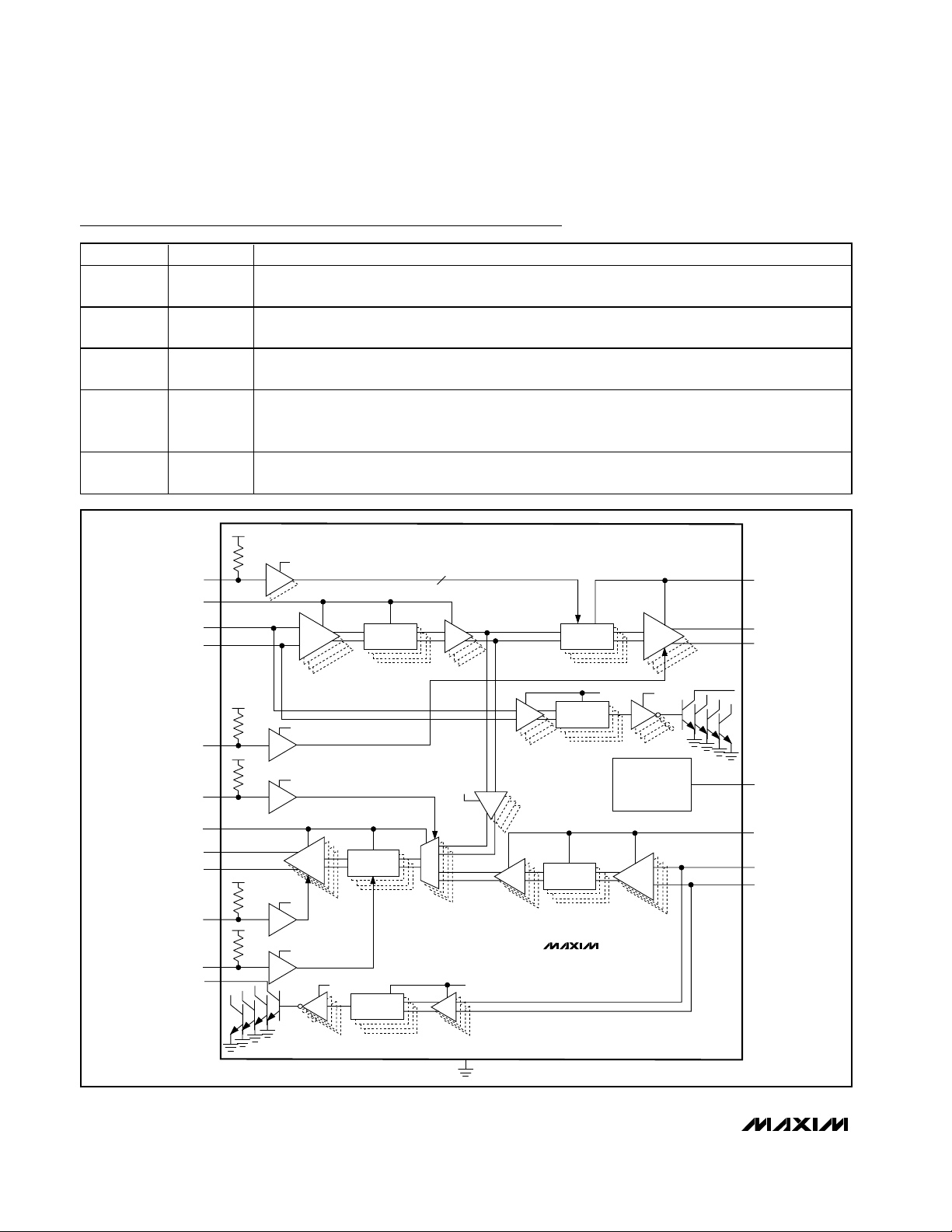
Figure 3. Functional Diagram
PIN NAME FUNCTION
55, 58, 61,64RX_OUT4+ to
RX_OUT1+
56, 59, 62,65RX_OUT4- to
RX_OUT1-
67 RX_PE
68 LOOPBACK
EP Exposed Pad
TX_PE[0:1]
V
CC
TX_IN[1:4]+
TX_IN[1:4]-
TX_ENABLE
LOOPBACK
PC Board Transmitter Positive Data Outputs, CML. These outputs are terminated with 50Ω to V
PC Board Transmitter Negative Data Outputs, CML. These outputs are terminated with 50Ω to V
PC Board Transmitter Preemphasis Control Input, LVTTL with 40kΩ Internal Pullup. Set high or open
to assert this bit.
Loopback Enable Input, LVTTL with 40kΩ Internal Pullup. Set low for normal operation. Set high or
open for internal connection of TX_IN to RX_OUT. TX_OUT continues to transmit when loopback is
enabled.
Exposed Pad. Signal and supply ground. For optimal high-frequency performance and thermal
conductivity, this pad must be soldered to the circuit board ground.
1
V
CC
40kΩ
1
1
V
CC
40kΩ
V
3
CC
40kΩ
LVTTL
LVTTL
LVTTL
V
VCC2
V
2
CC
CML
4
CC
FIXED
EQUALIZER
2
V
CC
LIMITER
4
PRE-
EMPHASIS
SIGNAL
DETECT
CML
V
CC
POWER
MANAGEMENT
2VCC1
V
2
CC
TX_OUT[1:4]+
TX_OUT[1:4]-
TX_SD[1:4]
POR
CC
CC
4.
4.
4
V
CC
RX_OUT[1:4]+
RX_OUT[1:4]-
RX_ENABLE
RX_PE
RX_SD[1:4]
PRE-
EMPHASIS
4
V
CC
SIGNAL
DETECT
LVTTL
LVTTL
CML
V
4
CC
V
4
CC
V
3
CC
40kΩ
3
V
CC
40kΩ
1
0
LIMITER
FIXED
EQUALIZER
CML
MAX3983
3
V
CC
GND
V
3
CC
RX_IN[1:4]+
RX_IN[1:4]-
Page 11

Detailed Description
The MAX3983 comprises a PC board receiver and
cable driver section (TX), as well as a cable receiver
and PC board driver section (RX). Equalization and signal detection are provided in each receiver, and preemphasis is included in each transmitter. The MAX3983
includes separate enable control for the TX outputs and
RX outputs. Loopback is provided for diagnostic testing.
PC Board Receiver and Cable Driver
(TX_IN and TX_OUT)
Data is fed into the MAX3983 from the host through a
CML input stage and fixed equalization stage. The
fixed equalizer in the PC board receiver corrects for up
to 20in of PC board loss on FR4 material. The cable driver includes four-state preemphasis to compensate for
up to 20m of 24AWG, 100Ω balanced cable. Table 1 is
provided for easy translation between preemphasis
expressions. Residual jitter of the MAX3983 is independent of up to 0.17UI
P-P
source jitter.
Cable Receiver and PC Board Driver
(RX_IN and RX_OUT)
The fixed equalizer on each RX input provides approximately 6dB equalization to correct for up to 5m of
28AWG, 100Ω balanced cable. The PC board driver
includes two-state preemphasis to compensate for up
to 20in of FR4 material.
Signal-Detect Outputs
Signal detect (SD) is provided on all eight data inputs.
Pullup resistors should be connected from the SD outputs to a supply in the 3.0V to 5.5V range. The signaldetect outputs are not valid until power-up is complete.
Typical signal-detect response time is 0.35µs.
In the RX section, the SD output asserts high when the
RX_IN signal amplitude is greater than 175mV
P-P
.
RX_SD deasserts low when the RX_IN signal amplitude
drops below 85mV
P-P
.
In the TX section, the SD output asserts high when the
TX_IN signal amplitude is greater than 800mV
P-P
.
TX_SD deasserts low when the TX_IN signal amplitude
drops below 200mV
P-P
.
TX and RX Enable
The TX_ENABLE and RX_ENABLE pins enable TX and
RX, respectively. Typical enable time is 15ns, and typical disable time is 25ns. The enable inputs may be
connected to signal-detect outputs to automatically
detect an incoming signal (see the Autodetect section).
Power-On Reset
To limit inrush current, the MAX3983 includes internal
power-on reset circuitry. Connect a capacitor 0.1µF ≤
C
POR
≤ 10µF from POR to ground. With C
POR
= 1µF,
power-on delay is 6ms (typ).
MAX3983
Quad Copper-Cable Signal Conditioner
______________________________________________________________________________________ 11
Table 1. Preemphasis Translation
RATIO αα
V
HIGH PP
V
LOW PP__
1.41 0.17 0.29 3
2.00 0.33 0.50 6
2.82 0.48 0.65 9
4.00 0.60 0.75 12
VV
HIGH PP LOW PP
VV
HIGH PP LOW PP
αα
__
−+
__
10Gbase-CX4 IN dB
1
−
V
LOW PP
V
HIGH PP
_
_
20 log
V
HIGH PP
V
LOW PP
_
_
V
LOW_PP
V
HIGH_PP
Page 12
MAX3983
Applications Information
Signal-Detect Output Leakage Current
Considerations
If all four RX or TX signal-detect outputs are to be connected together to form one signal detect, the leakage
current of the output stage needs to be considered.
Each SD output sinks a maximum of 25µA when asserted, so when four are connected together, a maximum of
100µA is possible. The value of the pullup resistor connected to pullup voltage V
PULLUP
should be selected so
the leakage current does not cause the output voltage to
fall below the threshold of the next stage. For example, if
the signal-detect outputs are connected together and to
a stage with a logic-high threshold of 1.5V, the pullup
resistor needs to be chosen so V
PULLUP
- I
LEAKAGE
x
R
PULLUP
> 1.5V. In this case, if V
PULLUP
= 3.0V,
R
PULLUP
should be less than 15kΩ.
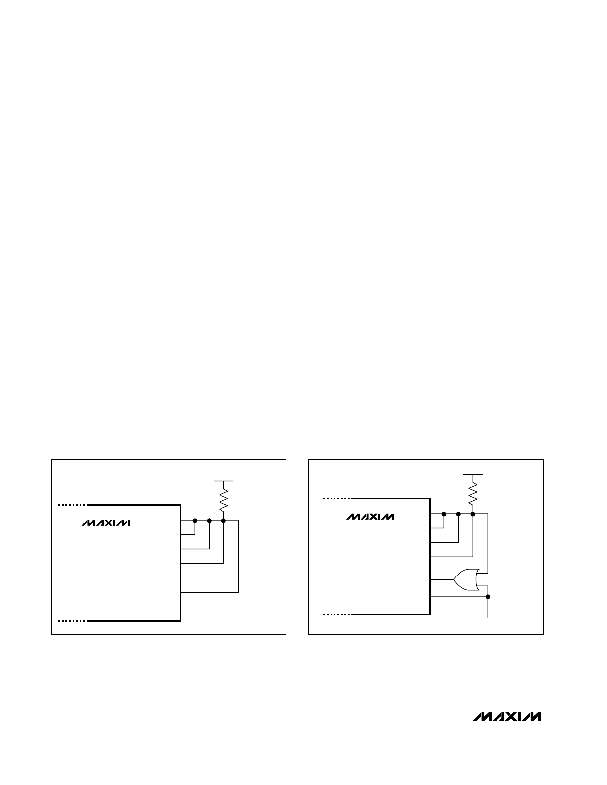
Autodetect
The MAX3983 can automatically detect an incoming signal and enable the appropriate outputs. Autodetect of
the RX side is done by connecting RX_SD[1:4] together
with a pullup resistor (value 4.7kΩ to 10kΩ to VCC) to
RX_ENABLE. For the TX side, this is done by connecting
TX_SD[1:4] together with a pullup resistor (value 4.7kΩ
to 10kΩ to VCC) to TX_ENABLE (Figure 4). If signal is
detected on all channels, SD is high and forces the corresponding ENABLE high. Leaving the inputs to the
MAX3983 open (i.e., floating) is not recommended, as
noise amplification can occur and create undesirable
output signals. Autodetect is recommended to eliminate
noise amplification or possible oscillation. When using
autodetect, the link length is determined by the received
signal strength. It is possible to reach longer distances if
the autodetect configuration is not used.
Using Loopback with Autodetect
If the MAX3983 is configured for autodetection,
RX_ENABLE is controlled by the RX_SD[1:4] outputs.
Since loopback requires RX_ENABLE to be high, a simple OR gate can be used to enable the RX outputs
when either RX_SD[1:4] is high or when LOOPBACK is
high (Figure 5).
InfiniBand and 10Gbase-CX4 Transition
Time Specification
InfiniBand specifies a minimum transition time (20% to
80%) of 100ps and CX4 specifies a minimum of 60ps.
Both are specified at the connector interface to the
cable. The output transition times of the MAX3983 are
45ps (typ) and therefore require some care to increase
this time. Approximately 3in of FR4 with 4-mil-wide lines
is sufficient to lengthen the transition time to 60ps. For
100ps transition times, additional length can be used or
an additional 1.5pF capacitor can be placed across the
outputs of the MAX3983. Do not use high-speed dielectric material for the circuit board if the application
requires the use of the InfiniBand or CX4 type connector
system. With such materials, the fast edges of the
Quad Copper-Cable Signal Conditioner
12 ______________________________________________________________________________________
Figure 4. Autodetection Using Corresponding Signal-Detect
Outputs and Enable Input
Figure 5. Loopback in Autodetect Mode
3.0V ≤ V
RX OR TX_SD1
MAX3983
RX OR TX_SD2
RX OR TX_SD3
RX OR TX_SD4
RX OR TX_ENABLE
≤ 5.5V
PULLUP
4.7kΩ ≤ R ≤ 10kΩ
RX_SD1
MAX3983
RX_SD2
RX_SD3
RX_SD4
RX_ENABLE
LOOPBACK
3.0V ≤ V
≤ 5.5V
PULLUP
4.7kΩ ≤ R ≤ 10kΩ
TO HOST
Page 13

MAX3983 will produce excessive crosstalk in InfiniBand
and CX4 cable assemblies.
Crosstalk
For InfiniBand and 10Gbase-CX4 applications, it is
imperative to know the near-end crosstalk characteristics
of the cable assemblies. 10Gbase-CX4 has defined the
upper limit over frequency for near-end crosstalk (NEXT)
with single and multiple aggressors. InfiniBand has only
specified a percentage as measured in the time domain
relative to the transmitter output. Regardless of the specification method, NEXT is a critical component of the link
performance. When using larger amounts of preemphasis, the received eye height is small and vulnerable to
NEXT. For those situations requiring a large transmit preemphasis, the NEXT should be less than -30dB at frequencies from 1GHz to 3GHz. It should be noted that
cables that meet the 10Gbase-CX4 NEXT and MDNEXT
should provide adequate isolation.
Layout Considerations
Circuit board layout and design can significantly affect
the performance of the MAX3983. Use good high-frequency design techniques, including minimizing
ground inductance and using controlled-impedance
transmission lines on the data signals. Power-supply
decoupling should also be placed as close to the V
CC
pins as possible. There should be sufficient supply filtering. Always connect all V
CC
s to a power plane. Take
care to isolate the input from the output signals to
reduce feedthrough. The performance of the equalizer
is optimized for lossy environments. For best results,
use board material with a dielectric tangential loss of
approximately 0.02 and 4-mil-wide transmission lines.
High-speed materials with tangential loss of less than
0.01 can be used, but require special care to reduce
near-end crosstalk in cable assemblies.
Exposed-Pad Package
The exposed-pad, 68-pin QFN package incorporates
features that provide a very low thermal resistance path
for heat removal from the IC. The pad is electrical
ground on the MAX3983 and must be soldered to the
circuit board for proper thermal and electrical performance. For more information on exposed-pad packages, refer to Maxim Application Note HFAN-08.1:
Thermal Considerations of QFN and Other ExposedPaddle Packages.
Interface Schematics
MAX3983
Quad Copper-Cable Signal Conditioner
______________________________________________________________________________________ 13
Figure 6. RX_IN and TX_IN Equivalent Input Structure
Figure 7. RX_OUT and TX_OUT Equivalent Output Structure
V
X
CC
RX_IN[1:4]+
TX_IN[1:4]+
50Ω
50Ω
RX_IN[1:4]TX_IN[1:4]-
GND
VCCX
50Ω
50Ω
5pF
V
X - 1.5V
CC
RX_OUT[1:4]+
TX_OUT[1:4]+
RX_OUT[1:4]TX_OUT[1:4]-
GND
Page 14

MAX3983
Quad Copper-Cable Signal Conditioner
14 ______________________________________________________________________________________
Figure 8. LVTTL Equivalent Input Structure
Figure 9. Signal-Detect Equivalent Output Structure
Y
V
CC
VCCX
Ω
40k
LVTTL IN
RX_SD[1:4]
TX_SD[1:4]
V
PIN NAME
RX_ENABLE,
LOOPBACK, RX_PE
TX_ENABLE,
TXPE[0:1]
XVCCY
CC
3VCC4
V
CC
1VCC2
V
CC
GND
GND
Page 15

MAX3983
Quad Copper-Cable Signal Conditioner
______________________________________________________________________________________ 15
Pin Configuration
Chip Information
TRANSISTOR COUNT: 7493
PROCESS: SiGe Bipolar
TOP VIEW
TX_SD1
TX_SD2
V
CC
TX_IN1-
TX_IN1+
GND
TX_IN2-
TX_IN2+
GND
TX_IN3-
TX_IN3+
GND
TX_IN4-
TX_IN4+
V
CC
TX_SD3
TX_SD4
4
CC
LOOPBACK
RX_PE
V
68 67 66 65 64 63 62 61
1
2
1
3
4
5
6
7
8
9
10
11
12
13
14
1
15
16
17
RX_OUT1-
RX_OUT1+
4
CC
V
RX_OUT3-
RX_OUT3+
4
CC
V
RX_OUT4-
4
CC
RX_OUT2-
RX_OUT2+
V
60 59 58 57 56 55 54 53 52
MAX3983
4
CC
RX_OUT4+
V
POR
RX_ENABLE
51
50
49
48
47
46
45
44
43
42
41
40
39
38
37
36
35
RX_SD1
RX_SD2
3
V
CC
RX_IN1+
RX_IN1-
GND
RX_IN2+
RX_IN2-
GND
RX_IN3+
RX_IN3-
GND
RX_IN4+
RX_IN4-
V
3
CC
RX_SD3
RX_SD4
18 19 20 21 22 23 24 25
N.C.
TX_ENABLE
2
CC
V
TX_OUT1-
TX_OUT1+
2
CC
V
26 27 28 29 30 31 32 33 34
TX_OUT2-
TX_OUT2+
2
CC
V
TX_OUT3-
TX_OUT3+
2
CC
V
TX_OUT4+
2
CC
V
TX_OUT4-
TX_PE0
TX_PE1
68 QFN*
*THE EXPOSED PAD OF THE QFN PACKAGE MUST BE SOLDERED TO GROUND
FOR PROPER THERMAL AND ELECTRICAL OPERATION OF THE MAX3983.
Page 16

MAX3983
Quad Copper-Cable Signal Conditioner
Maxim cannot assume responsibility for use of any circuitry other than circuitry entirely embodied in a Maxim product. No circuit patent licenses are
implied. Maxim reserves the right to change the circuitry and specifications without notice at any time.
16 ____________________Maxim Integrated Products, 120 San Gabriel Drive, Sunnyvale, CA 94086 408-737-7600
© 2003 Maxim Integrated Products Printed USA is a registered trademark of Maxim Integrated Products.
Package Information
(The package drawing(s) in this data sheet may not reflect the most current specifications. For the latest package outline information,
go to www.maxim-ic.com/packages
.)
68L QFN.EPS
PACKAGE OUTLINE, 68L QFN, 10x10x0.9 MM
21-0122
PACKAGE OUTLINE, 68L QFN, 10x10x0.9 MM
21-0122
C
C
1
2
1
2
 Loading...