

Page 1
General Description
The MAX3941 is designed to drive an electro-absorption modulator (EAM) at data rates up to 10.7Gbps. It
incorporates the functions of a biasing circuit and a
modulation circuit, with integrated control op amps
externally programmed by DC voltages.
The integrated bias circuit provides a programmable
biasing current up to 50mA. This bias current reflects a
bias voltage of up to 1.25V on an external 50Ω load. The
bias and modulation circuits are internally connected on
chip, eliminating the need for an external bias inductor.
A high-bandwidth, fully differential signal path is internally
implemented to minimize jitter accumulation. When a
clock signal is available, the integrated data-retiming
function can be selected to reject input-signal jitter.
The MAX3941 receives differential CML signals (ground
referenced) with on-chip line terminations of 50Ω. The
output has a 50Ω resistor for back termination and is
able to deliver a modulation current of 40mA
P-P
to
120mA
P-P
, with an edge speed of 23ps (20% to 80%
typ). This modulation current reflects an EAM modulation voltage of 1.0V
P-P
to 3.0V
P-P
.
The MAX3941 also includes an adjustable pulse-width
control circuit to precompensate for asymmetrical EAM
characteristics. It is available in a compact 4mm x
4mm, 24-pin thin QFN package and operates over the
-40°C to +85°C temperature range.
Features
♦ On-Chip Bias Network
♦ 23ps Edge Speed
♦ Programmable Modulation Voltage Up to 3V
P-P
♦ Programmable EAM Biasing Voltage Up to 1.25V
♦ Selectable Data-Retiming Latch
♦ Up to 10.7Gbps Operation
♦ Integrated Modulation and Biasing Functions
♦ 50Ω On-Chip Input and Output Terminations
♦ Pulse-Width Adjustment
♦ Enable and Polarity Controls
♦ ESD Protection
Applications
SONET OC-192 and SDH STM-64
Transmission Systems
DWDM Systems
Long/Short-Reach Optical Transmitters
10Gbps Ethernet
MAX3941
10Gbps EAM Driver with Integrated
Bias Network
________________________________________________________________ Maxim Integrated Products 1
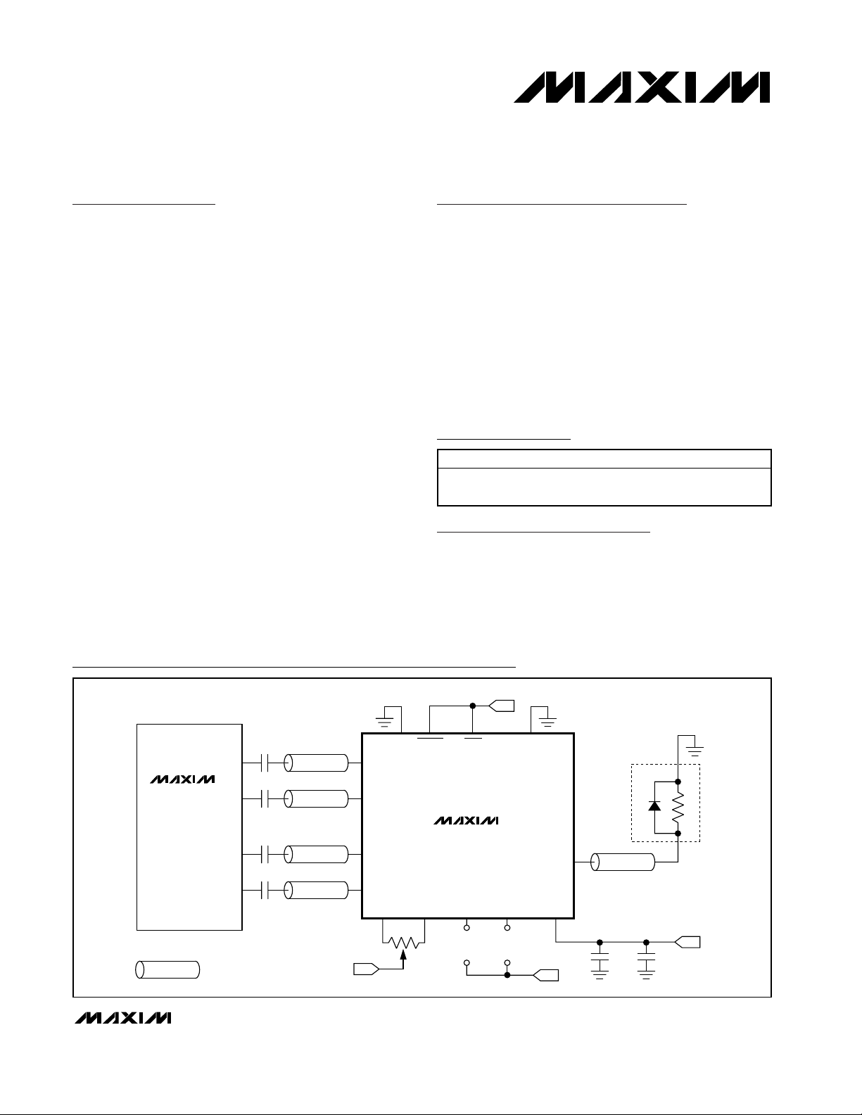
Typical Application Circuit
19-2935; Rev 0; 7/03
For pricing, delivery, and ordering information, please contact Maxim/Dallas Direct! at
1-888-629-4642, or visit Maxim’s website at www.maxim-ic.com.
Ordering Information
PART TEMP RANGE PIN-PACKAGE
MAX3941ETG -40°C to +85°C
24-Thin QFN
(4mm x 4mm)
-5.2V
MODEN
0.01µF
DATA+ DATA+
MAX3952
10Gbps
SERIALIZER
REPRESENTS A CONTROLLEDIMPEDANCE TRANSMISSION LINE.
0.01µF
DATA- DATA-
0.01µF
CLK+ CLK+
0.01µF
CLK- CLK-
50Ω
50Ω
50Ω
50Ω
-5.2V
PLRT GND
PWC+ PWC- V
2kΩ
RTEN
MAX3941
MODSET BIASSET
+
V
V
MODSET
BIASSET
-
EAM
OUT
EE
+
-
-5.2V
50Ω
330pF
-5.2V
0.1µF
Page 2
MAX3941
10Gbps EAM Driver with Integrated
Bias Network
2 _______________________________________________________________________________________
ABSOLUTE MAXIMUM RATINGS
Stresses beyond those listed under “Absolute Maximum Ratings” may cause permanent damage to the device. These are stress ratings only, and functional
operation of the device at these or any other conditions beyond those indicated in the operational sections of the specifications is not implied. Exposure to
absolute maximum rating conditions for extended periods may affect device reliability.
Supply Voltage V
EE
..............................................-6.0V to +0.5V
Voltage at MODEN,
RTEN, PLRT, MODSET, BIASSET ...........(V
EE
- 0.5V) to +0.5V
Voltage at DATA+, DATA-, CLK+, and CLK-……-1.65V to +0.5V
Voltage at OUT .............................................……….-4V to +0.5V
Voltage at PWC+, PWC- ...................(V
EE
- 0.5V) to (VEE+ 1.7V)
Current Into or Out of OUT.............................……………...80mA
Continuous Power Dissipation (T
A
= +85°C)
24-Lead Thin QFN
(derate 20.8mW/°C above +85°C).............................1354mW
Storage Temperature Range .....................……-55°C to +150°C
Operating Temperature Range ....................……-40°C to +85°C
Lead Temperature (soldering, 10s) .................................+300°C
ELECTRICAL CHARACTERISTICS
(VEE= -5.5V to -4.9V, TA= -40°C to +85°C. Typical values are at VEE= -5.2V, I
BIAS
= 30mA, I
MOD
= 100mA, and TA= +25°C, unless
otherwise noted.)
Power-Supply Voltage V
Supply Current I
Power-Supply Noise Rejection PSNR f ≤ 2MHz (Note 2) 15 dB
SIGNAL INPUT (Note 3)
Input Data Rates NRZ 10.7 Gbps
Single-Ended Input Resistance R
Single-Ended Input Voltage V
Differential Input Voltage V
Differential Input Return Loss RL
EAM BIAS
Maximum Bias Current V
Minimum Bias Current V
BIASSET Voltage Range V
Equivalent Bias Resistance R
Bias-Current-Setting Accuracy TA = +25°C
Bias-Current Temperature
Stability
BIASSET Input Resistance 20 kΩ
BIASSET Bandwidth
EAM MODULATION
Maximum Modulation Current 112 120 mA
Minimum Modulation Current V
MODSET Voltage Range V
E q ui val ent M od ul ati on Resi stance R
PARAMETER SYMBOL CONDITIONS MIN TYP MAX UNITS
EE
EE
BIASSET
BSEQV
Excluding I
(Note 1)
I
MOD
Input to GND 42.5 50 58.5 Ω
IN
DC-coupled, Figure 1a -1 0
IS
AC-coupled, Figure 1b -0.4 +0.4
DC-coupled (Note 4) 0.2 2.0
ID
AC-coupled (Note 4) 0.2 1.6
≤15GHz 15 dB
IN
BIASSET
BIASSET
(Note 5) 36.4 Ω
(Note 6)
50Ω driver load, V
Figure 2
MODSET
MODSET
MODEQV
(Note 7) 11.1 Ω
-5.5 -4.9 V
Retime disabled 124 174
and
BIAS
Retime enabled 140 201
= VEE + 2V 50 56 mA
= V
= V
EE
EE
V
BIASSET
V
BIASSET
V
BIASSET
V
BIASSET
V
BIASSET
BIASSET
V
EE
= VEE + 0.11V 2.1 4.3
= VEE + 0.36V 8.8 11.3
= VEE + 2.0V 52 58.4
< VEE + 0.36V -1100 +1100
≥ VEE + 0.36V -480 +480
= VEE + 0.55V,
V
EE
0.3 1.2 mA
VEE + 2 V
5MHz
37 40 mA
VEE + 1 V
mA
V
V
P-P
mA
ppm/°C
P-P
P-P
Page 3
MAX3941
10Gbps EAM Driver with Integrated
Bias Network
_______________________________________________________________________________________ 3
ELECTRICAL CHARACTERISTICS (continued)
(VEE= -5.5V to -4.9V, TA= -40°C to +85°C. Typical values are at VEE= -5.2V, I
BIAS
= 30mA, I
MOD
= 100mA, and TA= +25°C, unless
otherwise noted.)
Note 1: Supply current remains elevated once the retiming function is enabled. Power must be cycled to reduce supply
current after the retiming function is disabled.
Note 2: Power-supply noise rejection is specified as PSNR = 20log(V
noise (on Vcc)
/ ∆V
OUT
). V
OUT
is the voltage across a 50Ω load.
V
noise (on Vcc)
= 100mV
P-P
.
Note 3: For DATA+, DATA-, CLK+, and CLK-.
Note 4: CLK input characterized at 10.7Gbps.
Note 5: R
BSEQV
= (V
BIASSET
- VEE) / I
BIAS
with MODEN = VEE, DATA+ = high, and DATA- = low.
Note 6: Guaranteed by design and characterization using the circuit shown in Figure 4.
Note 7: R
MODEQV
= (V
MODSET
- VEE) / (I
MOD
- 37mA) with BIASSET = VEE.
Note 8: 50Ω load, characterized at 10.7Gbps with a 1111 1111 0000 0000 pattern.
Note 9: Deterministic jitter is defined as the arithmetic sum of pulse-width distortion (PWD) and pattern-dependent jitter (PDJ).
Measured with a 10.7Gbps 2
7
- 1 PRBS pattern with eighty 0s and eighty 1s inserted in the data pattern.
Note 10: For MODEN and PLRT.
Modulation Set Bandwidth
MODSET Input Resistance 20 kΩ
Modulation-Current Temperature
Stability
Modulation-Current-Setting Error 50Ω driver load, TA = +25°C -10 +10 %
Output Resistance R
Total Off Current
Output Return Loss RL
Output Edge Speed 20% to 80% (Notes 6, 8) 23 32 ps
Setup/Hold Time tSU, t
Pulse-Width Adjustment Range (Notes 6, 8) ±30 ±50 ps
Pulse-Width Control Input Range
(Single Ended)
Pulse-Width Control Input Range
(Differential)
Output Overshoot δ (Notes 6, 8) 10 %
Driver Random Jitter RJ
Driver Deterministic Jitter DJ
CONTROL INPUTS
Input High Voltage V
Input Low Voltage V
Input Current (Note 10) -80 +200 µA
PARAMETER SYMBOL CONDITIONS MIN TYP MAX UNITS
Modulation depth 10%, 50Ω driver load,
Figure 2
(Note 6) -957 0 ppm/°C
OUT
OUT to GND 42.5 50 58.5 Ω
BIASSET = V
V
, DATA+ = high, DATA- = low
EE
I
= 30mA,
OUT
DR
DR
IH
IL
BIAS
I
= 50mA
MOD
Figure 3 (Note 6) 25 ps
HD
For PWC+ and PWC-
(PWC+) - (PWC-) -0.5 +0.5 V
(Note 6) 0.3 0.7 ps
PWC- = GND (Notes 6, 9) 6.8 11 ps
(Note 10)
(Note 10)
, MODEN = VEE, MODSET =
EE
≤15GHz 10 dB
5 MHz
1.2 mA
V
+
EE
0.5
V
+
EE
2.0
VEE +
1.5
V
EE
0.8
+
V
RMS
P-P
V
V
Page 4
MAX3941
10Gbps EAM Driver with Integrated
Bias Network
4 _______________________________________________________________________________________
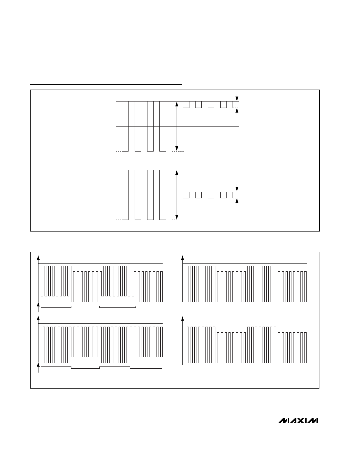
Figure 1. Definition of Single-Ended Input Voltage Range
Figure 2. Modulating BIASSET and MODSET Pins
Test Circuits and Timing Diagrams
0V
-0.5V
-1.0V
(a) DC-COUPLED SINGLE-ENDED CML INPUT
0.4V
0V
-0.4V
(b) AC-COUPLED SINGLE-ENDED (CML OR PECL) INPUT
0V
100mV
1.0V
800mV
100mV
0V
V
OUT
V
0V
NOTE: ALL AMPLITUDES ARE RELATIVE.
(a) MODULATING BIASSET
(b) MODULATING MODSET
BIASSET
V
OUT
V
MODSET
mW
(c) RESULT OF MODULATING BIASSET
AND MODSET 180° OUT OF PHASE
(d) RESULTING OPTICAL OUTPUT
V
OUT
P
OUT
Page 5

MAX3941
10Gbps EAM Driver with Integrated
Bias Network
_______________________________________________________________________________________ 5
Figure 3. Setup and Hold Timing Definition
Figure 4. AC-Characterization Circuit
Test Circuits and Timing Diagrams (continued)
CLK+
CLK-
DATA-
DATA+
(DATA+) -
(DATA-)
I
OUT
NOTE: I
OUT
t
SU
RELATES TO RETIMED DATA.
t
HD
VIS = 0.1V
DC-COUPLED
V
V
DC-COUPLED
I
MOD
I
BIAS
P-P
0.1V
P-P
AC-COUPLED
IS
= 0.2V
ID
P-P
0.2V
P-P
AC-COUPLED
= 40mA
= 0mA TO 50mA
TO 1V
TO 0.8V
TO 2V
TO 1.6V
TO 120mA
P-P
P-P
P-P
P-P
P-P
P-P
50Ω 50Ω
CLK+
CLK-
DATA+
DATA-
50Ω 50Ω
PATTERN
GENERATOR
-5.2V
50Ω
50Ω
50Ω
50Ω
0.1µF 300pF
GND PWC+
V
EE
RTEN
Q
D
I
MOD
50Ω
V
MODSET
GND1
V
EE
MODSET
R
OUT
50Ω
OUT
I
BIAS
V
EE
BIASSET
V
EE
V
EE
V
BIASSET
I
OUT
50Ω
Z
L
OSCILLOSCOPE
50Ω
PWC- GND GND2
50Ω
P
W
C
0
M
U
X
1
Page 6

MAX3941
10Gbps EAM Driver with Integrated
Bias Network
6 _______________________________________________________________________________________
Typical Operating Characteristics
(Typical values are at VEE= -5.2V, I
BIAS
= 30mA, I
MOD
= 100mA, TA= +25°C, unless otherwise noted.)
10Gbps ELECTRICAL EYE DIAGRAM
(V
MOD
= 1V
P-P
, 2
31
- 1 PRBS)
MAX3941 toc01
20ps/div
10Gbps ELECTRICAL EYE DIAGRAM
(V
MOD
= 3V
P-P
, 2
31
- 1 PRBS)
MAX3941 toc02
20ps/div
OC-192 OPTICAL EYE DIAGRAM
(OC-192 FILTER, 2
31
- 1 PRBS)
MAX3941 toc03
15ps/div
1
2
3
NOTE: BIAS AND MODULATION
SET AT OPTIMUM LEVELS FOR EAM.
Figure 5. Bias and Modulation Relationship to EAM Voltage
Test Circuits and Timing Diagrams (continued)
SUPPLY CURRENT vs. TEMPERATURE
(50Ω LOAD, EXCLUDES I
BIAS
, I
MOD
)
MAX3941 toc04
TEMPERATURE (°C)
I
EE
(mA)
80706050403020100-10-20-30
110
120
130
140
150
160
170
100
-40 90
RETIMING ENABLED
RETIMING DISABLED
PULSE WIDTH vs. R
PWC
MAX3941 toc05
R
PWC-
(Ω)
PULSE-WIDTH POSITIVE PULSE (ps)
2505001000 7501500 12501750
760
770
780
790
800
810
820
830
840
850
750
2000 0
R
PWC+
(Ω)
175015001000 1250500 7502500 2000
MEASURED AT 1.25Gbps
WITH A 1010 PATTERN
VOLTAGE
GND
V
OUT
VEE + 1.9V
V
BIAS
V
MOD
USABLE RANGE
BELOW USABLE RANGE
Page 7

MAX3941
10Gbps EAM Driver with Integrated
Bias Network
_______________________________________________________________________________________ 7
Typical Operating Characteristics (continued)
(Typical values are at VEE= -5.2V, I
BIAS
= 30mA, I
MOD
= 100mA, TA= +25°C, unless otherwise noted.)
PULSE-WIDTH DISTORTION
vs. TEMPERATURE
5.0
4.5
4.0
3.5
3.0
2.5
2.0
1.5
PULSE-WIDTH DISTORTION (ps)
1.0
0.5
0
-50 90
TEMPERATURE (°C)
V
BIAS
0
-0.2
-0.4
-0.6
(V)
-0.8
BIAS
V
-1.0
-1.2
-1.4
-1.6
0 2.5
vs. V
(ZL = 50Ω)
V
IS RELATIVE TO V
BIASSET
V
BIASSET
BIASSET
2.00.5 1.51.0
(V)
7050-10 10 30-30
EE
MAX3941 toc06
MAX3941 toc08
3.5
3.0
2.5
)
P-P
2.0
(V
MOD
1.5
V
1.0
0.5
0
0 1.00
30
25
20
15
PSNR (dB)
10
5
0
110
V
vs. V
MOD
MODSET
(ZL = 50Ω)
V
IS RELATIVE TO VEE.
MODSET
0.750.500.25
V
(V)
MODSET
POWER-SUPPLY NOISE REJECTION
vs. FREQUENCY
100
FREQUENCY (Hz)
1k
MAX3941 toc07
MAX3941 toc09
10k
DIFFERENTIAL S11 vs. FREQUENCY
(DEVICE POWERED)
0
-5
-10
-15
(dB)
1
-20
1
S
-25
-30
-35
-40
015
FREQUENCY (GHz)
9 1236
MAX3941 toc10
0
-4
-8
-12
-16
| (dB)
-20
22
|S
-24
-28
-32
-36
-40
03691215
S22 vs. FREQUENCY
(DEVICE POWERED)
MAX3941 toc11
FREQUENCY (GHz)
Page 8

MAX3941
Detailed Description
The MAX3941 EAM driver consists of two main parts: a
high-speed modulation driver and an EAM-biasing
block. The clock and data inputs to the driver are compatible with PECL and CML logic levels. The modulation and bias currents are output through the OUT pin.
The modulation output stage is composed of a highspeed differential pair and a programmable current
source with a maximum modulation current of 120mA.
The rise and fall times are typically 23ps. The modulation
current is designed to produce an EAM voltage up to
3.0V
P-P
when driving a 50Ω module. The 3.0V
P-P
results
from 120mA
P-P
through the parallel combination of the
50Ω EAM load and the internal 50Ω back termination.
Polarity Switch
The MAX3941 includes a polarity switch. When the
PLRT pin is high or left floating, the output maintains the
polarity of the input data. When the PLRT pin is low, the
output is inverted relative to the input data.
Clock/Data Input Logic Levels
The MAX3941 is directly compatible with ground-reference CML. Either DC- or AC-coupling can be used for
CML referenced to ground. For all other logic types,
AC-coupling should be used.
Optional Data Input Latch
To reject pattern-dependent jitter in the input data, a synchronous differential clock signal should be connected to
the CLK+ and CLK- inputs, and the RTEN control input
should be connected to VEE.
10Gbps EAM Driver with Integrated
Bias Network
8 _______________________________________________________________________________________
Pin Description
PIN NAME FUNCTION
1 DATA+ Noninverting Data Input with 50Ω On-Chip Termination
2 DATA- Inverting Data Input with 50Ω On-Chip Termination
3, 4, 14 GND Ground. All pins must be connected to board ground.
5 CLK+ Noninverting Clock Input for Data Retiming with 50Ω On-Chip Termination
6 CLK- Inverting Clock Input for Data Retiming with 50Ω On-Chip Termination
7, 11, 12, 13,
18, 19, 24
8 PWC+ Positive Input for Modulation Pulse-Width Adjustment (See the Design Procedure Section)
9 PWC-
10 MODSET Modulation Current Set. Apply a voltage to set the modulation current of the driver output.
15 GND1 Ground. Ground connection.
16 OUT Driver Output. Provides both modulation and bias output. DC-couple to EAM.
17 GND2 Ground. Ground connection.
20 PLRT
21 BIASSET Bias Current Set. Apply a voltage to set the bias current of the driver output.
22 MODEN
23 RTEN Data-Retiming Input. Connect to VEE for retimed data. Connect to GND to bypass retiming latch.
EP
Exposed
V
EE
Pad
Negative Supply Voltage. All pins must be connected to board VEE.
Negative Input for Modulation Pulse-Width Adjustment. Ground to disable the pulse-width
adjustment feature (see the Design Procedure section).
Differential Data Polarity Swap Input. Set high or float for normal operation. Set low to invert the
differential signal polarity. Contains an internal 100kΩ pullup to GND.
TTL/CMOS Modulation Enable Input. Set low or float for normal operation. Set high to put the EAM
in the absorption (logic 0) state. Contains an internal 100kΩ pulldown to V
Ground. Must be soldered to the circuit board ground for proper thermal and electrical performance
(see the Exposed Pad Package section).
EE
.
Page 9

The input data is retimed on the rising edge of CLK+. If
RTEN is connected to ground, the retiming function is disabled and the input data is directly connected to the output stage. Leave CLK+ and CLK- open when retiming is
disabled.
Pulse-Width Control
The pulse-width control circuit can be used to compensate for pulse-width distortion introduced by the EAM.
The differential voltage between PWC+ and PWCadjusts the pulse-width compensation. The adjustment
range is typically ±50ps. Optional single-ended operation is possible by forcing a voltage on the PWC+ pin
while leaving the PWC- pin unconnected. When PWCis connected to ground, the pulse-width control circuit
is automatically disabled.
Modulation Output Enable
The MAX3941 incorporates a modulation currentenable input. When MODEN is low or floating, the modulation/bias output (OUT) is enabled. When MODEN is
high, the output is switched to the logic 0 state. The
typical enable time is 2ns and the typical disable time
is 2ns.
Design Procedure
Programming the Modulation Voltage
The EAM modulation voltage results from I
MOD
passing
through the EAM impedance (ZL) in parallel with the
internal 50Ω termination resistor (R
OUT
):
To program the desired modulation current, force a
voltage at the MODSET pin (see the Typical Application
Circuit). The resulting I
MOD
current can be calculated
by the following equation:
An internal, independent current source drives a constant
37mA to the modulation circuitry, and any voltage above
VEEon the MODSET pin adds to this. The input impedance of the MODSET pin is typically 20kΩ. Note that the
minimum output voltage is V
EE
+ 1.9V (Figure 5).
Programming the Bias Voltage
As in the case of modulation, the EAM bias voltage
results from I
BIAS
passing through the EAM impedance
(Z
L
) in parallel with the internal 50Ω termination resistor
(R
OUT
):
To program the desired bias current, force a voltage at
the BIASSET pin (see the Typical Application Circuit).
The resulting I
BIAS
current can be calculated by the fol-
lowing equation:
The input impedance of the BIASSET pin is typically
20kΩ. Note that the minimum output voltage is VEE+
1.9V (Figure 5).
Programming the Pulse-Width Control
Three methods of control are possible when pulse predistortion is desired to minimize distortion at the receiver.
The pulse width can be set with a 2kΩ potentiometer with
the center tapped to VEE(or equivalent fixed resistors),
by applying a voltage to the PWC+ pin, or by applying a
differential voltage across the PWC+ and PWC- pins. See
Table 1 for the desired effect of the pulse-width setting.
Pulse width is defined as (positive pulse width)/((positive
pulse width + negative pulse width)/2).
Input Termination Requirement
The MAX3941 data and clock inputs are CML compatible. However, it is not necessary to drive the IC with a
standard CML signal. As long as the specified input voltage swings are met, the MAX3941 operates properly.
Applications Information
Layout Considerations
To minimize loss and crosstalk, keep the connections
between the MAX3941 output and the EAM module as
short as possible. Use good high-frequency layout
techniques and multilayer boards with an uninterrupted
ground plane to minimize EMI and crosstalk. Circuit
boards should be made using low-loss dielectrics. Use
controlled-impedance lines for the clock and data
inputs as well as for the data output. Be sure to filter the
power supply with capacitors placed close to the IC.
MAX3941
10Gbps EAM Driver with Integrated
Bias Network
_______________________________________________________________________________________ 9
Table 1. Pulse-Width Control
(
)
VI
≈×
MOD MOD
ZR
ZR
L OUT
×
L OUT
+
VI
≈×
BIAS BIAS
ZR
×
L OUT
ZR
+
L OUT
V
≈
BIASSET
64. Ω
3
I
BIAS
V
I
MOD
MODSET
≈+
11.1
37mA
Ω
PULSE-
WIDTH
(%)
100 R
>100 R
<100 R
R
R
PWC+
PWC+
PWC+
PWC+
PWC+
, R
+ R
PWCPWC-
= R
> R
< R
FOR
= 2kΩ
PWC-
PWC-
PWC-
V
PWC- OPEN
VEE + 1 0
> VEE + 1 >0
< VEE + 1 <0
PWC+
(V)
V
PWC+
V
-
PWC-
(V)
Page 10

MAX3941
Interface Schematics
Figures 7 and 8 show simplified input and output circuits of the MAX3941 EAM driver.
Exposed-Pad Package
The exposed pad on the 24-pin QFN provides a very low
thermal-resistance path for heat removal from the IC. The
pad is also electrically ground on the MAX3941 and must
be soldered to the circuit board for proper thermal and
electrical performance. Refer to Maxim Application Note
HFAN-08.1: Thermal Considerations for QFN and Other
Exposed-Pad Packages for additional Information.
Laser Safety and IEC 825
Using the MAX3941 EAM driver alone does not ensure
that a transmitter design is compliant with IEC 825. The
entire transmitter circuit and component selections must
be considered. Each customer must determine the level
of fault tolerance required by their application, recognizing that Maxim products are not designed or authorized
for use as components in systems intended for surgical
implant into the body, for applications intended to support or sustain life, or for any other application where the
failure of a Maxim product could create a situation where
personal injury or death may occur.
10Gbps EAM Driver with Integrated
Bias Network
10 ______________________________________________________________________________________
Figure 6. Functional Diagram
50Ω 50Ω
CLK+
CLK-
DATA+
DATA -
50Ω 50Ω
RTEN MODEN PLRT
V
EE
D0
Q
MUX
1
PWC+ PWC-
PWC
2kΩ
POLARITY
MAX3941
GND GND1 GND2
V
MODSET
+
-
50Ω
I
MOD
MODSET
V
EE
50Ω
R
50Ω
V
BIASSET
OUT
+
-
I
BIAS
BIASSET
50Ω
OUT
Z
L
V
EE
V
EE
V
EE
V
EE
Page 11

MAX3941
10Gbps EAM Driver with Integrated
Bias Network
Maxim cannot assume responsibility for use of any circuitry other than circuitry entirely embodied in a Maxim product. No circuit patent licenses are
implied. Maxim reserves the right to change the circuitry and specifications without notice at any time.
Maxim Integrated Products, 120 San Gabriel Drive, Sunnyvale, CA 94086 408-737-7600 ____________________ 11
© 2003 Maxim Integrated Products Printed USA is a registered trademark of Maxim Integrated Products.
Package Information
For the latest package outline information, go to www.maxim-
ic.com/packages.
Pin Configuration
Chip Information
Figure 7. Simplified Input Circuit
Figure 8. Simplified Output Circuit
TRANSISTOR COUNT: 1918
PROCESS: SiGe Bipolar
GND
50Ω 50Ω
DATA+/CLK+
DATA-/CLK-
V
EE
TOP VIEW
VEERTEN
24
23
1
DATA +
2
DATA -
GND
3
4
GND
5
CLK+
CLK-
6
7
8
EE.
V
PWC+
THIN QFN (4mm x 4mm)
EXPOSED PAD CONNECTED TO GROUND
MAX3941
MODEN
22
MAX3941
9
PWC-
BIASSET
21
10
MODSET
EE
PLRT
V
20
19
18
V
EE
17
GND2
16
OUT
15
GND1
14
GND
V
13
EE
11
12
EE
EE
V
V
GND1 GND2
MAX3941
50Ω
50Ω
GND OUT
50Ω
GND
V
EE
PART PACKAGE TYPE PACKAGE CODE
MAX3941ETG
24-Thin QFN
4mm x 4mm x 0.8mm
T2444-1
 Loading...