

Page 1
MAX3806
Receiver for Optical Distance Measurement
________________________________________________________________
Maxim Integrated Products
1
19-4700; Rev 0; 7/09
For pricing, delivery, and ordering information, please contact Maxim Direct at 1-888-629-4642,
or visit Maxim’s website at www.maxim-ic.com.
EVALUATION KIT
AVAILABLE
General Description
The MAX3806 is a high-gain linear preamplifier for distance measurement applications using a laser beam.
The device operates from a single +5.0V supply and
converts current from an AC-coupled photodiode into a
single-ended voltage signal. The input accepts single
pulses or bursts of pulses with widths down to 30ns.
The amplifier remains linear with input amplitudes from
42nAP(SNR = 3) to 40µAP. It can also withstand overload signals as large as 2mA
P
. The output stage is
designed to drive a high-impedance load to deliver the
output-voltage swing at the lowest possible power dissipation. The gain of the preamplifier stage is selected
using the GAIN pin to be 60kΩ or 30kΩ. There is also
an internal 14dB attenuator that is selected using the
ATT pin. The output stage can be disabled (high
impedance).
The device is available in a 3mm x 3mm, 12-pin TQFN
package and operates over the -40°C to +105°C temperature range.
Applications
LIDAR Sensors for Automotive Applications
(ACC, Stop&Go)
Laser Sensors for Portable Distance
Measurement
Laser Sensors for Industrial Applications
Features
♦ +5V Supply Voltage
♦ Linearity Range Up to 40µA
P
♦ Overload Current Up to 2mA
P
♦ 50mW Power Dissipation at +5.0V
♦ 1.5pA/
√
√
Hz Noise Density at 60kΩ Gain
♦ 14nA
RMS
Input-Referred Noise at 60kΩ Gain
♦ Selectable Gains (60kΩ, 30kΩ)
♦ Selectable 14dB Attenuation
Ordering Information
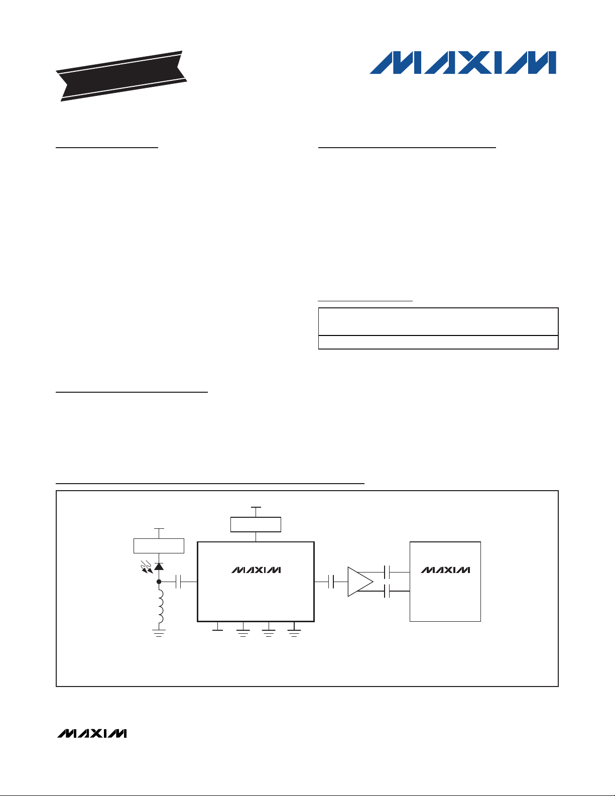
Typical Application Circuits
+
Denotes a lead(Pb)-free/RoHS-compliant package.
*
EP = Exposed pad.
PART TEMP RANGE
PIN-
PACKAGE
TOP
MARK
MAX3806GTC+ -40°C to +105°C 12 TQFN-EP* ABN
Pin Configuration appears at end of data sheet.
Typical Application Circuits continued at end of data sheet.
+5V TO +12V
SUPPLY FILTER
PIN
IN
C*
L*
* L AND C SET THE LOW-FREQUENCY CUTOFF REQUIRED FOR THE APPLICATION.
SUPPLY FILTER
LINEAR LIDAR Rx
GAIN
+5V
+5V
V
CC
MAX3806
SINGLE-CHANNEL RECEIVER
0.01μF
0.01μF
OUT
GNDATTDIS
BUFF
0.01μF
MAX1446
ADC
Page 2
MAX3806
Receiver for Optical Distance Measurement
2 _______________________________________________________________________________________
ABSOLUTE MAXIMUM RATINGS
ELECTRICAL CHARACTERISTICS
(VCC= +4.5V to +5.5V, AC-coupled (C = 0.01µF) output load ≥ 2kΩ, TA= -40°C to +105°C. Typical values are at VCC= +5V,
T
A
= +25°C, unless otherwise noted.) (Note 1)
Stresses beyond those listed under “Absolute Maximum Ratings” may cause permanent damage to the device. These are stress ratings only, and functional
operation of the device at these or any other conditions beyond those indicated in the operational sections of the specifications is not implied. Exposure to
absolute maximum rating conditions for extended periods may affect device reliability.
Supply Voltage Range, V
CC........................................
-0.5V to +6.0V
Voltage Range at ATT, DIS, GAIN
................
-0.5V to (VCC+ 0.5V)
Current Range at IN, OUT
...........................................
-4mA to +4mA
Continuous Power Dissipation (TA= +70°C)
12-Pin TQFN-EP (derate 16.7mW/°C above +70°C)...1333mW
Storage Temperature Range .............................-55°C to +150°C
Lead Temperature (soldering, 10s) .................................+300°C
Power-Supply C urrent ICC (Note 2) 10 15 mA
INPUT SPECIFICATIONS
Input-Referred Noise
Input-Referred Noise Den sity
Input Impedance
CMOS/TTL INPUT SPECIFICATIONS
Input High Voltage V
Input Low Voltage V
Input Current
Input Impedance
GENERAL SPECIFICATIONS
Small-Signal Transimpedance
Small-Signal Bandwidth f
Gain Peaking 5pF CIN 15pF 1 dB
Attenuation Stabil ity ATT = 1; 20log(V
OUTPUT SPECIFICATIONS
Total Harmonic Distortion THD
Power-Supply Noise Rejection
(Note 3)
PARAMETER S YMBOL CONDITIONS MIN TYP MAX UNITS
Output noise up to
100MHz/(gain at 5MHz)
Output noise centered
at 5MHz over 100H z
band/(gain at 5MHz)
At 1MH z, GAIN = 1 800
At 1MH z, GAIN = 0 300
2 VCC V
IH
0 0.8 V
IL
I
IH,IIL
I
IH
R
PULLUP
R
PULLDOWN
3dB
PSNR Noise frequency < 1MHz
DIS input ±150
GAIN and ATT inputs -180
DIS input 60
GAIN and ATT inputs 40
IIN 15μAP, GAIN = 1 44 60 77
50μAP, GAIN = 0 23 30 37
I
IN
CIN = 5pF
OUT_ATT_ ON/VOUT_ATT_OFF
Frequency = 1MHz,
= 0.5V
V
OUT
Frequency = 10MH z,
V
OUT
= 0.5V
P
P
CIN = 5pF, GAIN = 1 14 20
= 5pF, GAIN = 0 21 27
C
IN
CIN = 5pF, GAIN = 1 1.5 1.8
C
= 5pF, GAIN = 0 1.7 2.3
IN
GAIN = 1, ATT = 0 25 49
GAIN = 0, ATT = 0 55 98
) -13 -14 -15 dB
GAIN = 1 -54
GAIN = 0 -53
GAIN = 1 -38
GAIN = 0 -47
GAIN = 1 -16
GAIN = 0 -23
nA
RMS
pA/Hz
μA
k
k
MHz
dB
dB
Page 3
MAX3806
Receiver for Optical Distance Measurement
_______________________________________________________________________________________ 3
ELECTRICAL CHARACTERISTICS (continued)
(VCC= +4.5V to +5.5V, AC-coupled (C = 0.01µF) output load ≥ 2kΩ, TA= -40°C to +105°C. Typical values are at VCC= +5V,
T
A
= +25°C, unless otherwise noted.) (Note 1)
Note 1: AC specifications are guaranteed by design and characterization.
Note 2: Supply current is measured with OUT unterminated or AC-coupled.
Note 3: Measured by applying 100mV
P-P
sinusoidal noise to the supply voltage. PSNR is defined as 20log(V
OUT_NOISE/VCC_NOISE
).
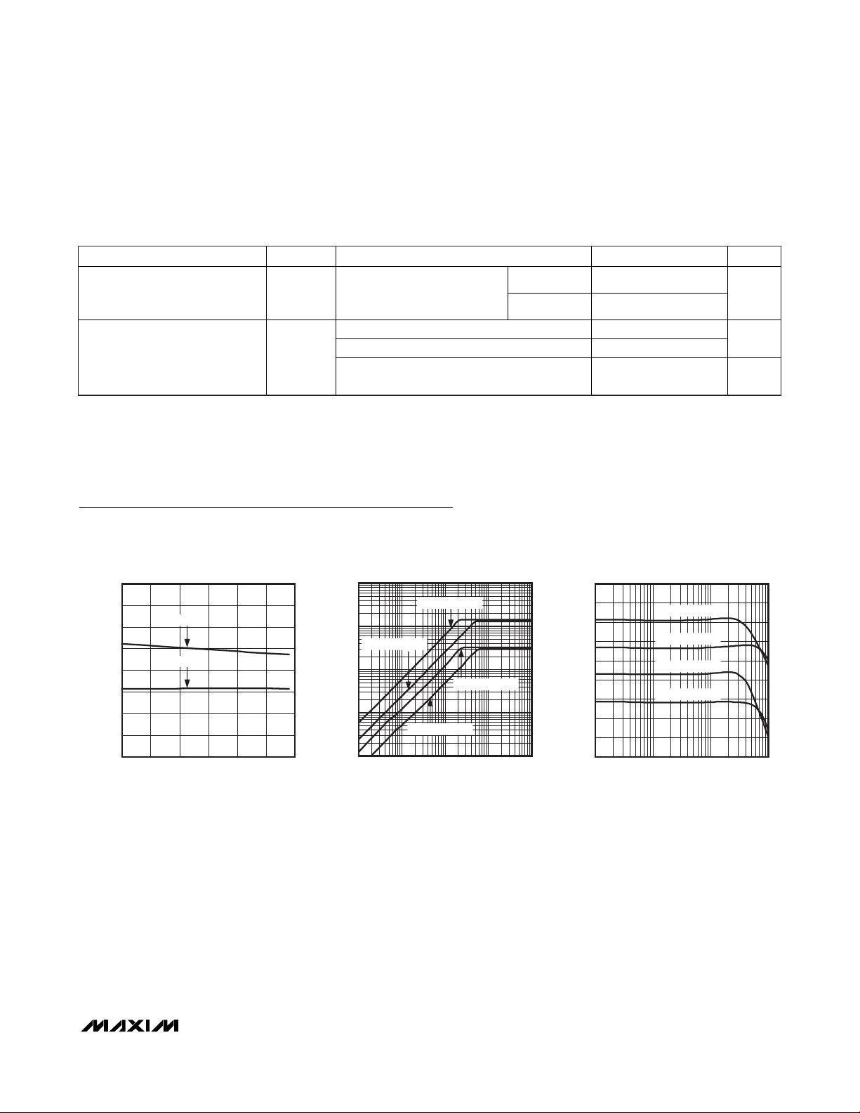
Typical Operating Characteristics
(Typical values are at VCC= +5V, TA= +25°C, CIN= 5pF, ATT = 0, unless otherwise noted.)
PARAMETER S YMBOL CONDITIONS MIN TYP MAX UNITS
Attenuation in Disable Mode
Output Impedance
Frequency < 5MHz,
20log(V
OUT_DISABLED
V
OUT_ENABLED
/
)
At 1MH z, DIS = 0, ATT = 0, GAIN = 0 or 1 51
At 1MH z, DIS = 0, ATT = 1, GAIN = 0 or 1 114
At 1MHz, DIS = 1, ATT = 0 or 1, GAIN = 0
or 1
ATT = 0 -71
dB
ATT = 1 -57
9 k
SUPPLY CURRENT vs. TEMPERATURE
16
14
12
10
8
6
SUPPLY CURRENT (mA)
4
2
0
-40 110
DIS = 0
DIS = 1
TEMPERATURE (NC)
OUTPUT VOLTAGE vs. INPUT CURRENT
10
MAX3806 toc01
)
1
P
GAIN = 0, ATT = 0
0.1
OUTPUT VOLTAGE (V
0.01
0.001
8560-15 10 35
0.1 1000
GAIN = 1, ATT = 0
GAIN = 1, ATT = 1
GAIN = 0, ATT = 1
100101
INPUT CURRENT (µAP)
MAX3806 toc02
105
100
95
90
85
80
75
TRANSIMPEDANCE (dBI)
70
65
60
FREQUENCY RESPONSE
GAIN = 1, ATT = 0
GAIN = 0, ATT = 0
GAIN = 1, ATT = 1
GAIN = 0, ATT = 1
0.1 100
FREQUENCY (MHz)
101
MAX3806 toc03
Page 4

MAX3806
Receiver for Optical Distance Measurement
4 _______________________________________________________________________________________
Typical Operating Characteristics (continued)
(Typical values are at VCC= +5V, TA= +25°C, CIN= 5pF, ATT = 0, unless otherwise noted.)
BANDWIDTH vs. INPUT CAPACITANCE
60
50
40
30
BANDWIDTH (MHz)
20
10
0
515
TA = -40 NC
INPUT CAPACITANCE (pF)
BANDWIDTH vs. INPUT CAPACITANCE
120
100
80
60
BANDWIDTH (MHz)
40
20
(GAIN = 1)
TA = +25 NC
TA = +105 NC
(GAIN = 0)
TA = -40NC
TA = +25NC
TA = +105NC
VCC = +5.0V
131197
VCC = +5V
MAX3806 toc04
MAX3806 toc07
BANDWIDTH vs. INPUT CAPACITANCE
GAIN PEAKING vs. INPUT
(GAIN = 1)
MAX3806 toc05
GAIN PEAKING (dB)
MAX3806 toc08
PSNR (dB)
1.0
0.8
0.6
0.4
0.2
GAIN = 1
0
515
POWER-SUPPLY NOISE REJECTION
(SUPPLY NOISE = 100mV
10
0
-10
-20
GAIN = 1, ATT = 1
-30
-40
-50
60
50
40
30
BANDWIDTH (MHz)
20
10
0
515
VCC = +5.5V
VCC = +5.0V
VCC = +4.5V
INPUT CAPACITANCE (pF)
TA = +25NC
131197
BANDWIDTH vs. INPUT CAPACITANCE
(GAIN = 0)
120
100
80
60
BANDWIDTH (MHz)
40
20
VCC = +5.5V
VCC = +5.0V
VCC = +4.5V
TA = +25NC
CAPACITANCE
GAIN = 0
INPUT CAPACITANCE (pF)
GAIN = 1, ATT = 0
GAIN = 0, ATT = 0
GAIN = 0, ATT = 1
131197
P-P
MAX3806 toc06
)
MAX3806 toc09
MAX3806 toc11
-60
10k 10M
FREQUENCY (Hz)
OUTPUT-REFERRED NOISE
vs. INPUT CAPACITANCE
)
OUTPUT-REFERRED NOISE (µV
1000
RMS
950
900
850
800
750
700
650
600
TA = +25NC
INPUT CAPACITANCE (pF)
0
515
INPUT CAPACITANCE (pF)
131197
INPUT-REFERRED NOISE
vs. INPUT CAPACITANCE
16
)
15
RMS
14
13
12
INPUT-REFERRED NOISE (nA
11
10
515
VCC = +5V
TA = +105NC
TA = -40NC
TA = +25NC
INPUT CAPACITANCE (pF)
GAIN = 1
BW = 100MHz
131197
MAX3806 toc10
0
515
INPUT-REFERRED NOISE
vs. INPUT CAPACITANCE
16
)
15
RMS
14
13
12
INPUT-REFERRED NOISE (nA
11
10
515
INPUT CAPACITANCE (pF)
TA = +25NC
VCC = +5.5V
VCC = +5.0V
VCC = +4.5V
INPUT CAPACITANCE (pF)
131197
GAIN = 1
BW = 100MHz
131197
1M100k
GAIN = 1
BW = 100MHz
VCC = +5.5V
VCC = +5.0V
VCC = +4.5V
1311975
MAX3806 toc12
15
Page 5

MAX3806
Receiver for Optical Distance Measurement
_______________________________________________________________________________________
5
µ
Typical Operating Characteristics (continued)
(Typical values are at VCC= +5V, TA= +25°C, CIN= 5pF, ATT = 0, unless otherwise noted.)
INPUT-REFERRED NOISE
vs. INPUT CAPACITANCE
26
25
)
RMS
24
23
22
21
20
INPUT-REFERRED NOISE (nA
19
18
VCC = +5V
TA = +105NC
INPUT CAPACITANCE (pF)
TA = +25NC
TA = -40NC
0
-10
-20
-30
THD (dB)
-40
GAIN = 0
BW = 100MHz
131197515
26
25
)
MAX3806 toc13
RMS
24
23
22
21
20
INPUT-REFERRED NOISE (nA
19
18
TOTAL HARMONIC DISTORTION
vs. FREQUENCY
V
GAIN = 1
GAIN = 0
INPUT-REFERRED NOISE
vs. INPUT CAPACITANCE
TA = +25NC
VCC = +5.5V
INPUT CAPACITANCE (pF)
= 0.5V
OUT
P
MAX3806 toc16
VCC = +5.0V
VCC = +4.5V
GAIN = 0
BW = 100MHz
131197515
MAX3806 toc14
(DC-BLOCK = 0.01
DIS
(5V/div)
OUT
(200mV/div)
OUTPUT-REFERRED NOISE
700
)
RMS
650
600
550
500
OUTPUT-REFERRED NOISE (µV
450
DISABLE SWITCH
vs. INPUT CAPACITANCE
TA = +25NC
VCC = +5.5V
VCC = +5.0V
515
INPUT CAPACITANCE (pF)
F, LOAD = 2kI)
MAX3806 toc17
VCC = +4.5V
GAIN = 0
BW = 100MHz
131197
MAX3806 toc15
-50
-60
0.1 100
FREQUENCY (MHz)
GAIN SWITCH
(DC-BLOCK = 0.01µF, LOAD = 2kI)
GAIN
(5V/div)
OUT
(200mV/div)
40µs/div
101
100ns/div
ATT SWITCH
MAX3806 toc18
(5V/div)
(500mV/div)
(DC-BLOCK = 0.01µF, LOAD = 2kI)
ATT
OUT
40µs/div
MAX3806 toc19
Page 6

MAX3806
Receiver for Optical Distance Measurement
6 _______________________________________________________________________________________
Functional Diagram
Typical Operating Characteristics (continued)
(Typical values are at VCC= +5V, TA= +25°C, CIN= 5pF, ATT = 0, unless otherwise noted.)
TRANSIENT RESPONSE
(LINEAR REGION, GAIN = 1)
1µA
60mV
P
P
IN
OUT
20ns/div
MAX3806 toc20
20MHz BW LIMIT
TRANSIENT RESPONSE
(OVERLOAD REGION, GAIN = 1)
2mA
P
IN
OUT
1.4V
P
MAX3806
MAX3806 toc21
ZOOM IN
IN
OUT
20MHz BW LIMIT
100ns/div
ATTENUATORIN OUT
TRANSIENT RESPONSE
(OVERLOAD REGION, GAIN = 1)
2mA
P
60µs SETTLING TIME
1.4V
P
0.01µF DC-BLOCK
2kI LOAD
10µs/div
MAX3806 toc22
ZOOM OUT
V
SWITCHABLE
IMPEDANCE
60kΩ OR 30kΩ
40kΩ 40kΩ
GAIN ATT DIS
CC
60kΩ
Page 7

MAX3806
Receiver for Optical Distance Measurement
_______________________________________________________________________________________ 7
Detailed Description
The MAX3806 preamplifier consists of a selectable-gain
transimpedance amplifier, a selectable 14dB attenuator,
and an output-driver block. The selectable-gain transimpedance amplifier linearly boosts the signal from the
photodiode. This block is followed by an attenuator
block that allows the user to attenuate the signal by
14dB selected by the ATT pin. The final block is the output driver that can be disabled by asserting the DIS pin.
Transimpedance Amplifier
The selectable-gain transimpedance amplifier is controlled by the GAIN pin. See Table 1 for gain settings.
Attenuator
The attenuator block can be set to pass the signal
through to the output stage with 0dB of attenuation
(ATT forced low) or with 14dB of attenuation (ATT
forced high).
Output Driver
The output driver is designed to drive an AC-coupled
load with an impedance of 2kΩ or greater. The output
can be disabled by asserting the DIS pin high. When
the output is disabled, the OUT pin goes to a highimpedance state. See Figure 1 for the equivalent output
circuit.
WARNING: The output is designed to be AC-coupled
to a high-impedance load. Operating the part with its
output DC-coupled to GND through a 2kΩ or less load
may damage the output.
Applications Information
Settling Time
Settling time is the required time for the output to
achieve the final steady-state or AC amplitude swing
after a setting has been changed on the MAX3806. The
output common-mode voltage shifts when a change is
Pin Description
Table 1. Transimpedance Gain Settings
PIN NAME FUNCTION
1, 12 VCC 5V Power-Supply Connection
2 IN Amplifier Input. Accepts AC-coupled photodiode input current.
3, 4 GND Supply Ground
5 ATT
6, 8, 11 N.C. Not Connected. This pin is not internally connected.
7 GAIN
9 OUT
10 DIS
— EP
CMOS/TTL Input. A ss ert this pin high to enable a 14dB attenuator in the amplifier. Force this pin low
to disable the attenuator. Contains internal 40k pul ldown resistor. Connect to GND if not used.
CMOS/TTL Input. Selects amplifier gain setting. Force high for 60k . Force low for 30k. Contains
internal 40k pulldown resistor.
Ampl ifier Output. An increa se in current into the IN pin cau ses the voltage at the OUT pin to decrease.
OUT must be AC-coupled to a load of 2k or greater.
CMOS/TTL Input. Force high to disable the output of the MAX3806. Force low to enable the output.
Contains internal 60k pullup resistor.
Exposed Pad. The exposed pad must be soldered to circuit board ground for proper thermal and
electrical performance.
GAIN TRANSIMPEDANCE (k) LINEAR RANGE (μAP) BANDWIDTH (MHz)
0 30 IIN 40 98
1 60 IIN 20 49
Page 8

MAX3806
Receiver for Optical Distance Measurement
8 _______________________________________________________________________________________
made to either the GAIN or ATT setting. Table 2 provides typical output common-mode voltages for the
combination of settings. Settling time is proportional to
the RC time constant set by the output DC-blocking
capacitor, load, and MAX3806 output impedance. For
example, a 0.01µF DC-blocking capacitor, 2kΩ load,
and 51Ω output impedance provide an RC time constant of approximately 20µs. After changing the GAIN
or ATT setting, the system should wait at least three to
four time constants before analyzing received signals.
Settling time is also required when changing the DIS
setting. When DIS is asserted high, the output disables
to high impedance and typically settles to steady state
within 200ns. When DIS is deasserted, the output
enables and typically settles to steady state within 50ns.
Overload Recovery Time
Transistors saturate when the amplifier is overloaded,
resulting in output distortion. Overload typically occurs
with signals greater than 20µAP(GAIN = 1) or 40µA
P
(GAIN = 0). It can withstand overload signals as large
as 2mAP. Recovery time depends on the amplitude and
duration of the overload pulse.
Layout Considerations
Noise performance and bandwidth are adversely affected by capacitance at the IN pad. Minimize capacitance
on this pad and select a low-capacitance photodiode.
Reducing PCB capacitance can be accomplished by
removing the ground plane underneath the connection
from the photodiode to the IN pin and by keeping the
photodiode as close as possible to the MAX3806.
Use broadband power-supply filtering techniques to
achieve the best sensitivity and noise performance.
Exposed-Pad Package and Thermal
Considerations
The exposed pad on the 12-pin TQFN provides a very
low thermal resistance path for heat removal from the IC.
The pad is also electrical ground on the MAX3806 and
must be soldered to the circuit board ground for proper
thermal and electrical performance. Refer to Application
Note 862:
HFAN-08.1: Thermal Considerations of QFN
and Other Exposed-Paddle Packages
for additional
information.
Pin Configuration
PACKAGE TYPE PACKAGE CODE DOCUMENT NO.
12 TQFN-EP T1233+1
21-0136
Figure 1. Equivalent Output Circuit
Table 2. Output Common-Mode Voltages
Package Information
For the latest package outline information and land patterns, go
to www.maxim-ic.com/packages
.
V
CC
200Ω
V
CC
400Ω OUT
100Ω
TOP VIEW
OUT
7
8
9
10 6 N.C.DIS
11 5N.C. ATT
12 4V
CC
*EXPOSED PAD
MAX3806
+
2
1
IN N.C.
CC
V
THIN QFN
(3mm × 3mm)
*EP
3
GND GAIN
GND
GAIN ATT
0 0 1.65
0 1 0.33
1 0 1.82
1 1 0.36
OUTPUT COMMON-MODE
VOLTAGE (V)
Page 9

MAX3806
Receiver for Optical Distance Measurement
Maxim cannot assume responsibility for use of any circuitry other than circuitry entirely embodied in a Maxim product. No circuit patent licenses are
implied. Maxim reserves the right to change the circuitry and specifications without notice at any time.
Maxim Integrated Products, 120 San Gabriel Drive, Sunnyvale, CA 94086 408-737-7600 _____________________
9
© 2009 Maxim Integrated Products Maxim is a registered trademark of Maxim Integrated Products, Inc.
Typical Application Circuits (continued)
+5V
+5V TO +12V
SUPPLY FILTER
PIN
C*
L*
+5V TO +12V
SUPPLY FILTER
PIN
C*
L*
+5V TO +12V
SUPPLY FILTER
PIN
C*
L*
+5V TO +12V
SUPPLY FILTER
PIN
C*
L*
* L AND C SET THE LOW-FREQUENCY CUTOFF REQUIRED FOR THE APPLICATION.
IN
IN
IN
IN
GAIN
+5V
GAIN
+5V
GAIN
+5V
GAIN
+5V
SUPPLY FILTER
V
CC
MAX3806
LINEAR LIDAR Rx
+5V
SUPPLY FILTER
V
CC
MAX3806
LINEAR LIDAR Rx
+5V
SUPPLY FILTER
V
CC
MAX3806
LINEAR LIDAR Rx
+5V
SUPPLY FILTER
V
CC
MAX3806
LINEAR LIDAR Rx
0.01μF
OUT
GNDATTDIS
DIS0
0.01μF
OUT
GNDATTDIS
DIS1
0.01μF
OUT
GNDATTDIS
DIS2
0.01μF
OUT
GNDATTDIS
DIS3
+5V
7kΩ
3kΩ
MULTIPLE-CHANNEL RECEIVER
+5V
7kΩ
3kΩ
+5V
7kΩ
3kΩ
+5V
7kΩ
3kΩ
+5V
MAX4311
4:1 MUX/AMP
IN0
IN1
IN2
IN3
DIS0
DIS1
DIS2
DIS3
A1A0
0.01μF
BUFF
MICROCONTROLLER/DSP
0.01μF
MAX1446
ADC
0.01μF
 Loading...