

Page 1
General Description
The MAX3805 is designed to provide up to 30in
(0.75m) reach on 6-mil differential FR-4 transmission
line, or up to 24ft (8m) on RG-188A/U type coaxial
cable, for PRBS data from 9.95Gbps to 10.7Gbps. The
MAX3805 adaptive equalizer reduces intersymbol interference, resulting in 20ps residual jitter after equalization. An internal feedback network controls the
equalizer to automatically match frequency-dependent
skin effect and dielectric losses. The MAX3805 provides LVCMOS-compatible output-enable and signaldetect functions.
The MAX3805 has separate supply connections for the
internal logic and I/O circuits. This allows the currentmode logic (CML) input and CML output to be connected to isolated supplies for independent DC-coupled
interfaces to 1.8V, 2.5V, or 3.3V ICs. The MAX3805
comes in a very small 3mm x 3mm package and consumes only 135mW.
Applications
OC-192, 10GbE Switches and Routers
OC-192, 10GbE Serial Modules
High-Speed Signal Distribution
Features
♦ 3mm x 3mm Package
♦ Spans 30in (0.75m) of 6-mil FR-4
♦ Spans 24ft (8m) of Coax
♦ Automatic Receive Equalization to Reduce ISI
Caused by Path Losses
♦ Up to 10.7Gbps NRZ Data Operating Range
♦ Signal-Detect Output
♦ Output-Enable Control
♦ 135mW Power Consumption
♦ DC-Coupled Input and Output to Terminations as
Low as 1.65V
♦ Differential or Single-Ended Operation
♦ +3.3V Core Power Supply
MAX3805
10.7Gbps Adaptive Receive Equalizer
________________________________________________________________ Maxim Integrated Products 1
Ordering Information
19-2936; Rev 0; 7/03
For pricing, delivery, and ordering information, please contact Maxim/Dallas Direct! at
1-888-629-4642, or visit Maxim’s website at www.maxim-ic.com.
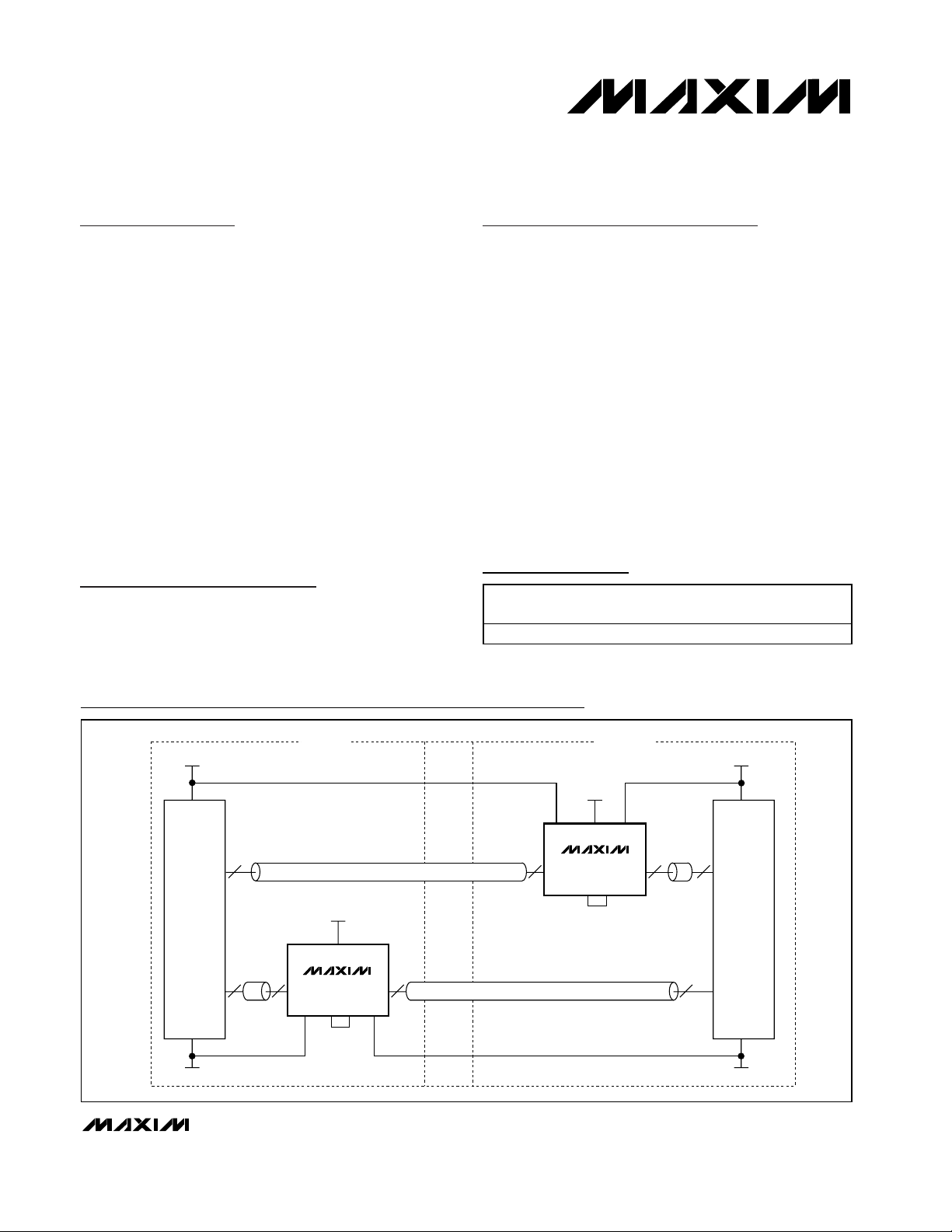
Typical Operating Circuit
Pin Configuration appears at end of data sheet.
PART TEMP RANGE
MAX3805ETE -40°C to +85°C 16 Thin QFN T1633F-3
PINPACKAGE
PACKAGE
CODE
LINE CARD SWITCH CARD
2.5V
+3.3V
10Gbps
CDR/SERDES
Tx
2
+3.3V
22
Rx
2.5V
SDO
V
CC2
MAX3805
SD EN
V
CC
FR-4 STRIPLINE
2
SDI
V
CC1
PC BOARD
BACKPLANE
V
CC1VCCVCC2
SDI
2
FR-4 STRIPLINE
MAX3805
SD EN
SDO
2
2
1.8V
10Gbps
SWITCH
Rx
2
Tx
1.8V
Page 2
MAX3805
10.7Gbps Adaptive Receive Equalizer
2 _______________________________________________________________________________________
ABSOLUTE MAXIMUM RATINGS
ELECTRICAL CHARACTERISTICS
(Pin 13 (HFPD) and pin 14 (LFPD) are not connected. Typical values are at VCC= +3.3V, V
CC1
= V
CC2
= 1.8V, TA= +25°C, unless
otherwise noted.) (Values at -40°C are guaranteed by design and characterization.)
Stresses beyond those listed under “Absolute Maximum Ratings” may cause permanent damage to the device. These are stress ratings only, and functional
operation of the device at these or any other conditions beyond those indicated in the operational sections of the specifications is not implied. Exposure to
absolute maximum rating conditions for extended periods may affect device reliability.
Supply Voltage (VCC) ............................................-0.5V to +4.0V
CML Supply Voltage
(V
CC1
, V
CC2
) ..........................................-0.5V to (VCC+ 0.5V)
Current at SDO±...............................................................±25mA
SDI±, EN, SD, HFPD, LFPD........................-0.5V to (V
CC
+ 0.5V)
Current at HFPD, LFPD ......................................................400µA
Continuous Power Dissipation (T
A
= +85°C)
16-Lead QFN-EP (derate 17.5mW/°C
above +85°C) ............................................................1398mW
Operating Ambient Temperature Range .............-40°C to +85°C
Storage Ambient Temperature Range...............-55°C to +150°C
Lead Temperature (soldering, 10s) .................................+300°C
OPERATING CONDITIONS
Supply Voltage V
Input Termination Voltage V
Output Termination Voltage V
PARAMETER SYMBOL CONDITIONS MIN TYP MAX UNITS
CC
CC1
CC2
3.0 3.3 3.6 V
1.65 V
1.65 V
CC
CC
Operating Ambient Temperature -40 +25 +85 °C
Supply Current I
CML Input Differential Voltage V
PARAMETER SYMBOL CONDITIONS MIN TYP MAX UNITS
CC
VCC = V
AC-coupled or DC-coupled at transmission
IN
line input (Notes 1, 6)
CC1
= V
CC2
CML Input Common-Mode
Voltage
CML Input Resistance Differential 85 100 115 Ω
CML Input Return Loss 100MHz to 10GHz 10 dB
CML Output Differential Voltage V
OUT
V
= 1.65V to 3.6V 400 500 600 mV
CC2
CML Output Resistance Differential 85 100 115 Ω
CML Output Transition Time tr/t
20% to 80% (Notes 2, 6) 35 ps
f
CML Output Return Loss 100MHz to 5GHz 10 dB
Equalizer Time Constant 10 µs
Output Residual Jitter (Notes 3–6) 21 30 ps
Signal-Detect Assert PRBS2
Signal-Detect Deassert PRBS2
LVCMOS Input-High Leakage
Current
I
H
31
- 1 at 10.7Gbps (Note 1) 200 mV
31
- 1 at 10.7Gbps (Note 1) 220 mV
41 60 mA
400 1200 mV
1.3 V
CC1
+10 +60 µA
V
V
P-P
V
P-P
P-P
P-P
P-P
Page 3
MAX3805
10.7Gbps Adaptive Receive Equalizer
_______________________________________________________________________________________ 3
Note 1: Differential input sensitivity is defined at the input to a transmission line with path length up to 30in.
Note 2: Measured using 10 ones and 10 zeros at 10.7Gbps.
Note 3: Residual jitter is the difference in total jitter between the signal at the input to the transmission line and the equalizer output.
Total residual jitter is DJ
P-P
+ 14.1 × RJ
RMS
.
Note 4: Measured at 10.7Gbps using a pattern of 100 ones, PRBS 2
10
- 1, 100 zeros, PRBS 2
10
- 1.
Note 5: V
IN
= 400mV
P-P
to 1200mV
P-P
, input path is 0 to 30in, 6-mil microstrip in FR-4, εr= 4.5, and tan δ = 0.02.
Note 6: Guaranteed by design and characterization.
ELECTRICAL CHARACTERISTICS (continued)
(Pin 13 (HFPD) and pin 14 (LFPD) are not connected. Typical values are at VCC= +3.3V, V
CC1
= V
CC2
= 1.8V, TA= +25°C, unless
otherwise noted.) (Values at -40°C are guaranteed by design and characterization.)
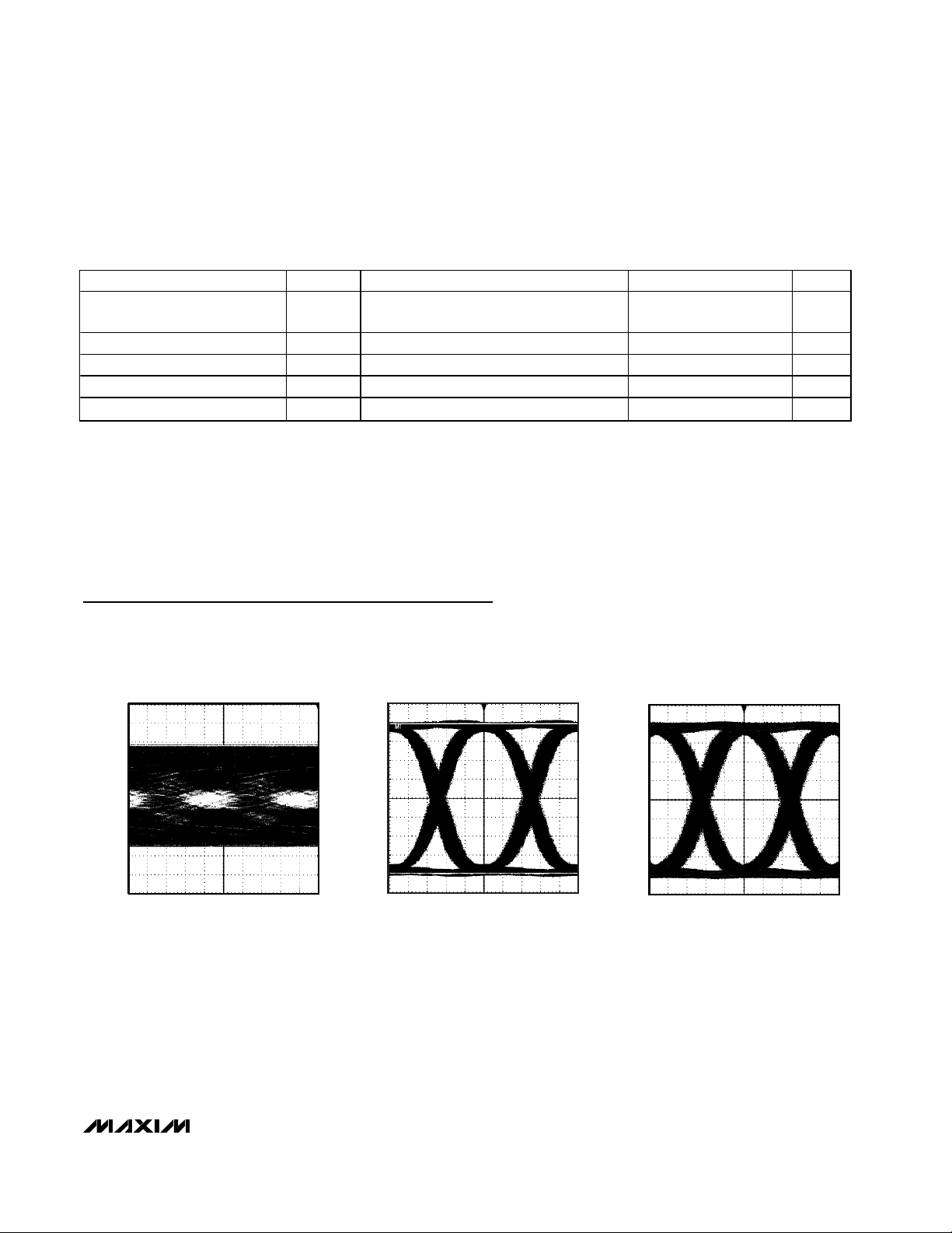
Typical Operating Characteristics
(VCC= 3.3V, V
CC1
= 1.8V, V
CC2
= 1.8V, and TA= +25°C, unless otherwise noted.)
EQUALIZER INPUT EYE AFTER 30in OF FR-4
(2
10
- 1PRBS WITH 100 CIDs AT 9.953Gbps)
MAX3805 toc01
20ps/div
65mV/div
EQUALIZER OUTPUT EYE AFTER 30in OF FR-4
(2
31
- 1PRBS AT 10.7Gbps)
MAX3805 toc03
20ps/div
65mV/div
LVCMOS Input-Low Leakage
Current
LVCMOS Input High V
LVCMOS Input Low V
LVCMOS Output High V
LVCMOS Output Low V
PARAMETER SYMBOL CONDITIONS MIN TYP MAX UNITS
I
L
IH
IL
OH
IOH = 12.5µA 2.1 V
IOL = 0.5mA 0.2 V
OL
-30 +30 µA
1.5 V
0.5 V
EQUALIZER OUTPUT EYE AFTER 30in OF FR-4
10
- 1PRBS WITH 100 CIDs AT 9.953Gbps)
(2
MAX3805 toc02
65mV/div
20ps/div
Page 4

MAX3805
10.7Gbps Adaptive Receive Equalizer
4 _______________________________________________________________________________________
Typical Operating Characteristics (continued)
(VCC= 3.3V, V
CC1
= 1.8V, V
CC2
= 1.8V, and TA= +25°C, unless otherwise noted.)
EQUALIZER OUTPUT EYE AFTER 30in OF FR-4
(CJTPAT 10.0Gbps LFPD/(HFPD + LFPD) = 0.6)
MAX3805 toc04
EQUALIZER OUTPUT EYE AFTER
24ft OF RG-188/U COAXIAL CABLE,
SINGLE ENDED (2
23
- 1PRBS AT 10.7Gbps)
MAX3805 toc05
SUPPLY CURRENT vs. TEMPERATURE
65
VCC = V
60
CC1
= V
CC2
= +3.3V
MAX3805 toc06
65mV/div
50
45
40
35
30
RESIDUAL JITTER (ps)
25
20
15
400 1200
50
45
40
35
30
25
RESIDUAL JITTER (ps)
20
15
10
65mV/div
20ps/div
RESIDUAL JITTER vs. AMPLITUDE
DATA RATE = 9.953Gbps
PATTERN = PRBS 2
RESIDUAL JITTER = DJ + 14.1 x RJ
FR4 = 18in
10
-1
FR4 = 30in
AMPLITUDE (mV
11001000900800700600500
)
P-P
RESIDUAL JITTER vs. DATA RATE
VIN = 400mV
PATTERN = 100 1's PRBS 210-1
100 0's PRBS 2
RESIDUAL JITTER = DJ + 14.1 x RJ
6 7 8 9 10 11
P-P
30in FR4
DATA RATE (Gbps)
10
-1
18in FR4
MAX3805 toc07
MAX3805 toc09
20ps/div
55
50
45
SUPPLY CURRENT (mA)
40
35
-40 -20 0 20 40 60 80
RESIDUAL JITTER
vs. FR-4 PATH LENGTH
50
DATA RATE = 10.7Gbps
PATTERN = PRBS 2
45
= 400mV
V
IN
40
35
30
RESIDUAL JITTER
25
20
RESIDUAL JITTER = DJ + 14.1 x RJ
15
39126 151821242730
10
-1
P-P
FR-4 PATH LENGTH (in)
RESIDUAL JITTER
/(R
vs. R
R
LFPD
LFPD
50
45
40
35
30
RESIDUAL JITTER (ps)
25
20
RESIDUAL JITTER = DJ + 14.1 x RJ
15
0.5 0.9
+ R
HFPD
VIN = 400mV
PATTERN = CJTPAT
DATA RATE = 10.0Gbps
+ R
(R
LFPD
HFPD
18in FR4
/(R
+ R
HFPD
LFPD
TEMPERATURE (°C)
)
LFPD
P-P
) = 100k
Ω
30in FR4
0.80.70.6
)
MAX3805 toc08
MAX3805 toc10
Page 5

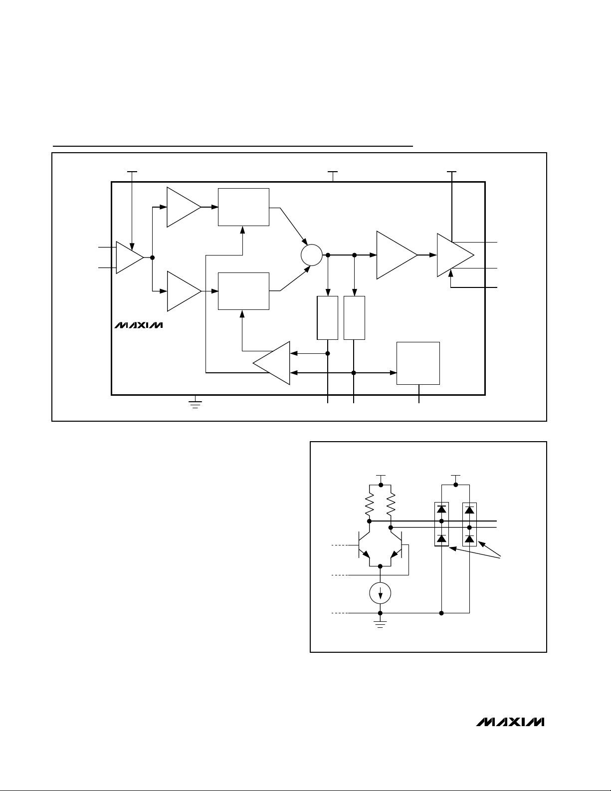
Detailed Description and
Applications Information
The MAX3805 adaptive equalizer is designed to operate with 9.95Gbps to 10.7Gbps PRBS nonreturn-to-zero
(NRZ) data at the receive end of a transmission line,
typically differential 6-mil FR-4 PC board. It adaptively
corrects intersymbol interference caused by frequencydependent path loss. It can also be used with coaxial
cable links and with transmission lines that include wellengineered connectors, as long as the total path loss is
relatively smooth and does not exceed 20dB at 5GHz.
The signal path for the MAX3805 consists of a CML
input stage, two amplifiers feeding a pair of variable
attenuators controlled by feedback, and a limiting
amplifier with a CML output stage. An enable input, EN,
is used to control the output stage. A signal-detect output, SD, indicates when input signal to the transmission
line is above 220mV
P-P
or below 200mV
P-P
, typically.
See the Functional Diagram.
CML Input and Output Buffers
The MAX3805 CML input and output buffers are internally terminated with 50Ω to V
CC1
and V
CC2
, respectively. The input and output circuitry have separate
voltage connections to control noise coupling and provide DC-coupling to +1.8V, +2.5V, or +3.3V CML. If
desired, the CML inputs and outputs can be AC-coupled. See Figure 1 for the output structure.
The low-frequency cutoff of the input-stage offset-cancellation circuit is nominally 21kHz.
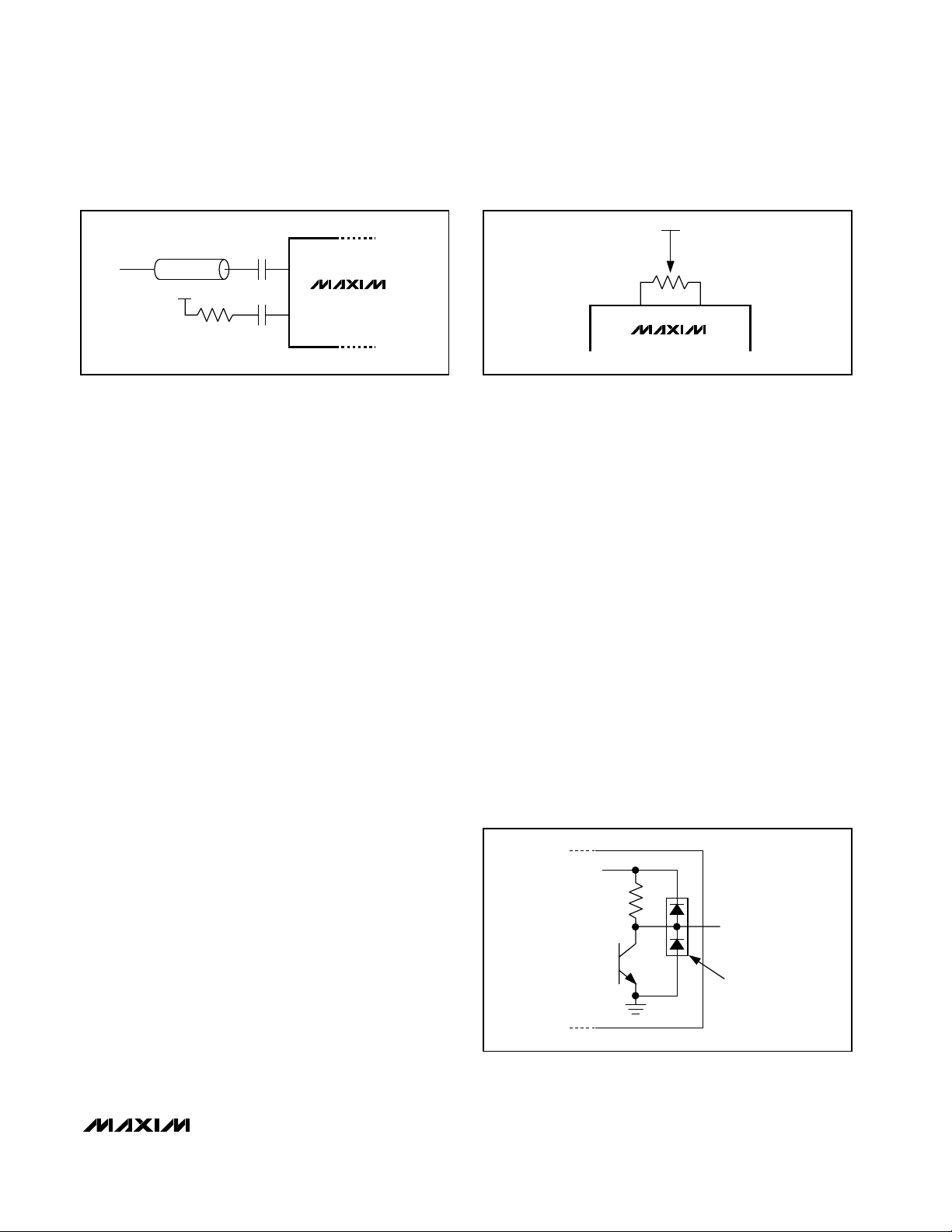
For single-ended operation (typically coaxial cable
links), the input must be AC-coupled; connect the
unused input to V
CC1
using a series combination of an
AC-coupling capacitor and a 50Ω resistor, as shown in
Figure 2. Note that the MAX3805 is specified for differential operation, and the performance may be reduced
in single-ended operation.
MAX3805
10.7Gbps Adaptive Receive Equalizer
_______________________________________________________________________________________ 5
Pin Description
PIN NAME FUNCTION
1V
2 SDI+ Positive Differential Serial Data Input, CML
3 SDI- Negative Differential Serial Data Input, CML
4V
5 GND Supply Ground
6 SD Signal-Detect Output, LVCMOS. Low indicates <200mV
7 EN Enable Input, LVCMOS. Low disables output, high enables output, typically connected to SD.
8 GND Supply Ground
9, 12 V
10 SDO- Negative Differential Serial Data Output, CML
11 SDO+ Positive Differential Serial Data Output, CML
13 HFPD High-Frequency Power Detector. Leave open for 9.953Gbps to 10.7Gbps PRBS NRZ data.
14 LFPD Low-Frequency Power Detector. Leave open for 9.953Gbps to 10.7Gbps PRBS NRZ data.
15 V
16 GND Supply Ground
EP
CC1
CC1
CC2
Exposed
Pad
Supply Voltage, CML Input (1.8V to VCC)
Supply Voltage, CML Input (1.8V to VCC)
, high indicates >220mV
P-P
Supply Voltage, CML Output (1.8V to VCC)
Supply Voltage, Equalizer Core, 3.3V
CC
Ground. The exposed pad must be soldered to the circuit board ground plane for proper thermal and
electrical performance.
P-P
.
Page 6
MAX3805
Input Stage with Equalization
The low-noise input stage of the MAX3805 includes two
amplifiers, one with flat frequency response and the
other with a highpass frequency response compensating for the loss characteristic of 6-mil FR-4 PC board
transmission line. A current-steering network, implemented with a pair of variable attenuators feeding into a
common summing node, provides the means to continuously vary the amount of equalization. The amount of
equalization is controlled by feedback from two powerdetector blocks that set the variable attenuators to
match the loss of a particular transmission path.
Dual Power-Detector Feedback Loop
The MAX3805 adapts the equalizer to a specific path
loss by sampling the output of the summing node with a
pair of frequency-dependent power detectors. The first
power detector has a lowpass bandwidth of 500MHz; the
second power detector has full bandwidth.
NRZ PRBS data has a sin2(f)/f2spectral characteristic.
When this data is passed through a lossy FR-4 path,
high-frequency components are attenuated, while low-
10.7Gbps Adaptive Receive Equalizer
6 _______________________________________________________________________________________
Functional Diagram
Figure 1. CML Output Structure
V
CC1
V
CC
V
CC2
VARIABLE
ATTENUATOR
VARIABLE
ATTENUATOR
SDI+
CML IN
SDI-
FLAT
AMP
BOOST
AMP
MAX3805
LOOP
FILTER
∑
LF POWER
LFPD HFPD
POWER
DETECTOR
LIMITING
DETECTOR
V
CC2
AMP
50Ω50Ω
SIGNAL
DETECT
SD
CML OUT
V
CC
SDO+
SDO-
EN
OUT+
OUT-
ESD
STRUCTURES
Page 7
frequency components remain essentially intact. These
changes in the spectral characteristic of the signal at
the output of the path are measured with the two power
detectors to provide a means to determine the path
loss.
The dual power-detector feedback loop measures the
ratio between the outputs of the two power detectors
and adjusts the attenuation to restore the sin2(f)/f
2
characteristic. The time constant for this feedback loop
is nominally 10µs.
Operating with Different Data Rates and
Codes
The MAX3805 equalizer feedback loop is optimized for
9.95Gbps to 10.7Gbps NRZ PRBS data; however, it
can also be used at a lower data rate or with a different
coding type by adjusting the feedback loop. The relative gain of the two power detectors can be adjusted by
connecting a 500kΩ trimmer potentiometer between
HFPD and LFPD pins, with the wiper connected to VCC,
as shown in Figure 3. Set the trimmer potentiometer for
the best eye opening.
Adding the potentiometer between HFPD and LFPD
can change the assert and deassert levels of the signal
detector, which could render the signal-detect output
invalid. For normal operation with 9.953Gbps to
10.7Gbps PRBS NRZ data, these signals should be left
open with no connections to pin 13 (HFPD) or pin 14
(LFPD). Note that excessive capacitance on pin 13 or
pin 14 can affect the operation of the feedback loop.
Make certain that the PC board traces from these pins
to the trimmer potentiometer are kept short.
Enable Function
The EN output is an LVCMOS-compatible pin that
enables the output stage of the MAX3805. Connect EN
to V
CC
or LVCMOS high to enable the output stage of
the device or to GND or LVCMOS low to disable the
output stage of the device.
Signal Detect
The output of the high-frequency power detector is
used to generate an LVCMOS-compatible signal-detect
(SD) output. The SD output asserts when the input signal at the transmission line falls below 200mV
P-P
, and
deasserts when the input signal at the transmission line
rises above 220mV
P-P
. The SD output can be directly
connected to the EN input to disable the MAX3805 output when no data signal is available. The SD output has
an LVCMOS fanout of one.
Package and Layout Considerations
The MAX3805 is packaged in a 3mm x 3mm plasticencapsulated 16-lead thin QFN package with exposed
pad for signal integrity. The exposed pad provides thermal and electrical connectivity to the IC, and must be
soldered to a high-frequency ground plane. Use good
layout techniques for the10Gbps SDI and SDO PC
board transmission lines, and configure the trace geometry near the IC package to minimize impedance discontinuities. Power-supply decoupling capacitors
should be provided for each supply connection and
located as close as practical to the IC package.
MAX3805
10.7Gbps Adaptive Receive Equalizer
_______________________________________________________________________________________ 7
50Ω
Figure 2. Single-Ended Operation
Figure 3. Connecting a Potentionmeter Across HFPD and LFPD
Figure 4. Signal-Detect Output Circuit
TRANSMISSION LINE
V
CC1
50Ω
V
CC
0.01µF
500kΩ
MAX3805
0.01µF
IN+
IN-
MAX3805
LFPD HFPD
V
CC
60kΩ
SD
ESD
STRUCTURES
Page 8
MAX3805
10.7Gbps Adaptive Receive Equalizer
8 _______________________________________________________________________________________
Pin Configuration
Chip Information
TRANSISTOR COUNT: 1647
PROCESS: SiGe Bipolar
VCCLFPD
GND
16 15 14 13
1
V
CC1
2
SDI+
3
SDI-
4
V
CC1
*EXPOSED PAD IS CONNECTED TO GND
MAX3805
5678
SD
GND
HFPD
V
12
CC2
SDO+
11
SDO-
10
V
9
CC2
EN
GND
Page 9

MAX3805
10.7Gbps Adaptive Receive Equalizer
Package Information
(The package drawing(s) in this data sheet may not reflect the most current specifications. For the latest package outline information,
go to www.maxim-ic.com/packages
.)
_______________________________________________________________________________________ 9
C
L
D2
b
D
D/2
E/2
- A -
- B -
C
L
0.10
0.08
C
C
A
A2
A1
E
(NE - 1) X e
C
L
e
D2/2
e
L
0.10 M C A B
E2/2
k
(ND - 1) X e
C
L
e
E2
L
L
12x16L QFN THIN.EPS
PROPRIETARY INFORMATION
TITLE:
PACKAGE OUTLINE
12 & 16L, QFN THIN, 3x3x0.8 mm
21-0136
REV.DOCUMENT CONTROL NO.APPROVAL
1
C
2
Page 10

MAX3805
10.7Gbps Adaptive Receive Equalizer
Maxim cannot assume responsibility for use of any circuitry other than circuitry entirely embodied in a Maxim product. No circuit patent licenses are
implied. Maxim reserves the right to change the circuitry and specifications without notice at any time.
10 ____________________Maxim Integrated Products, 120 San Gabriel Drive, Sunnyvale, CA 94086 408-737-7600
© 2003 Maxim Integrated Products Printed USA is a registered trademark of Maxim Integrated Products.
Package Information (continued)
(The package drawing(s) in this data sheet may not reflect the most current specifications. For the latest package outline information,
go to www.maxim-ic.com/packages
.)
EXPOSED PAD VARIATIONS
NOTES:
1. DIMENSIONING & TOLERANCING CONFORM TO ASME Y14.5M-1994.
2. ALL DIMENSIONS ARE IN MILLIMETERS. ANGLES ARE IN DEGREES.
3. N IS THE TOTAL NUMBER OF TERMINALS.
4. THE TERMINAL #1 IDENTIFIER AND TERMINAL NUMBERING CONVENTION SHALL CONFORM TO
JESD 95-1 SPP-012. DETAILS OF TERMINAL #1 IDENTIFIER ARE OPTIONAL, BUT MUST BE LOCATED
WITHIN THE ZONE INDICATED. THE TERMINAL #1 IDENTIFIER MAY BE EITHER A MOLD OR
MARKED FEATURE.
5. DIMENSION b APPLIES TO METALLIZED TERMINAL AND IS MEASURED BETWEEN 0.20 mm AND 0.25 mm
FROM TERMINAL TIP.
6. ND AND NE REFER TO THE NUMBER OF TERMINALS ON EACH D AND E SIDE RESPECTIVELY.
7. DEPOPULATION IS POSSIBLE IN A SYMMETRICAL FASHION.
8. COPLANARITY APPLIES TO THE EXPOSED HEAT SINK SLUG AS WELL AS THE TERMINALS.
9. DRAWING CONFORMS TO JEDEC MO220 REVISION C.
PROPRIETARY INFORMATION
TITLE:
PACKAGE OUTLINE
12 & 16L, QFN THIN, 3x3x0.8 mm
APPROVAL
DOCUMENT CONTROL NO.
21-0136
REV.
2
C
2
 Loading...