

Page 1
General Description
The MAX3799 is a highly integrated limiting amplifier
and VCSEL driver that operates up to 14Gbps, making
it suitable for Ethernet and Fibre Channel applications.
By providing a selectable data path with a noise-shaping filter, the MAX3799 enables a module with 10G
optics to be fully compliant with both 1000BASE-SR
and 10GBASE-SR specifications. Operating from a single +3.3V supply, this low-power integrated limiting
amplifier and VCSEL driver IC enables a platform
design for SFP MSA as well as for SFP+ MSA-based
optical transceivers. The high-sensitivity limiting amplifier limits the differential input signal generated by a
transimpedance amplifier into a CML-level differential
output signal. The compact VCSEL driver provides a
modulation and a bias current for a VCSEL diode. The
optical average power is controlled by an average
power control (APC) loop implemented by a controller
that interfaces to the VCSEL driver through a 3-wire
digital interface. All differential I/Os are optimally backterminated for a 50Ω transmission line PCB design.
The use of a 3-wire digital interface reduces the pin
count while enabling advanced Rx (rate selection, LOS
threshold, LOS squelch, LOS polarity, CML output level,
signal path polarity, deemphasis, and fast mode-select
change time) and Tx settings (modulation current, bias
current, polarity, and eye safety control) without the
need for external components. The MAX3799 provides
multiple current and voltage DACs to allow the use of
low-cost controller ICs.
The MAX3799 is packaged in a lead-free, 5mm x 5mm,
32-pin TQFN package.
Applications
1000BASE-SR/10GBASE-SR Multirate SFP+
Optical Transceiver
1x/2x/4x/8x/16x SFF/SFP/SFP+ MSA Fibre
Channel (FC) Optical Transceiver
Features
♦ Enables Single-Module Design Compliance with
1000BASE-SR and 10GBASE-SR Specifications
♦ -21.5dBm Optical Sensitivity at 1.25Gbps Using a
10.32Gbps ROSA (-19.7dBm OMA)
♦ Low Power Dissipation of 320mW at 3.3V Power
Supply
♦ Typical Electrical Performance of 14.025Gbps on
Rx/Tx (Non-Retimed 16x Fibre Channel Solution)
♦ 3mV
P-P
Receiver Sensitivity at 10.32Gbps
♦ 4ps
P-P
DJ at Receiver Output at 8.5Gbps 8B/10B
♦ 4ps
P-P
DJ at Receiver Output at 10.32Gbps
2
31
- 1 PRBS
♦ 26ps Rise and Fall Time at Rx/Tx Output
♦ Rate Select for 1Gbps Mode or 10Gbps Mode
♦ CML Output Squelch
♦ Polarity Select for Rx and Tx
♦ LOS Assert Level Adjustment
♦ LOS Polarity Select
♦ Modulation Current Up to 12mA Into 100Ω
Differential Load
♦ Bias Current Up to 15mA
♦ Integrated Eye Safety Features
♦ 3-Wire Digital Interface
♦ Programmable Deemphasis at Tx Output
MAX3799
1Gbps to 14Gbps, SFP+ Multirate Limiting
Amplifier and VCSEL Driver
________________________________________________________________
Maxim Integrated Products
1
Ordering Information
19-4695; Rev 0; 8/09
For pricing, delivery, and ordering information, please contact Maxim Direct at 1-888-629-4642,
or visit Maxim’s website at www.maxim-ic.com.
EVALUATION KIT
AVAILABLE
+
Denotes a lead(Pb)-free/RoHS-compliant package.
*
EP = Exposed pad.
PART TEMP RANGE PIN-PACKAGE
MAX3799ETJ+ -40°C to +85°C 32 TQFN-EP*
Typical Application Circuit and Pin Configuration appear at
end of data sheet.
Page 2
MAX3799
1Gbps to 14Gbps, SFP+ Multirate Limiting
Amplifier and VCSEL Driver
2 _______________________________________________________________________________________
ABSOLUTE MAXIMUM RATINGS
ELECTRICAL CHARACTERISTICS
(VCC= 2.85V to 3.63V, TA= -40°C to +85°C, CML receiver output load is AC-coupled to differential 100Ω, CAZ= 1nF, transmitter output load is AC-coupled to differential 100Ω (see Figure 1), typical values are at +25°C, V
CC
= 3.3V, I
BIAS
= 6mA, I
MOD
= 6mA, unless
otherwise specified. Registers are set to default values unless otherwise noted, and the 3-wire interface is static during measurements. For testing, the RATE_SEL bit was used and the RSEL pin was left open.)
Stresses beyond those listed under “Absolute Maximum Ratings” may cause permanent damage to the device. These are stress ratings only, and functional
operation of the device at these or any other conditions beyond those indicated in the operational sections of the specifications is not implied. Exposure to
absolute maximum rating conditions for extended periods may affect device reliability.
V
CCR
, V
CCT
, V
CCD
.................................................-0.3V to +4.0V
Voltage Range at DISABLE, SDA, SCL, CSEL,
RSEL, FAULT, BMON, LOS, CAZ2.........-0.3V to (VCC+ 0.3V)
Voltage Range at ROUT+, ROUT- .....(VCC- 1V) to (VCC+ 0.3V)
Voltage at TIN+, TIN-........................(V
CC
- 2.5V) to (VCC- 0.5V)
Voltage Range at TOUT+, TOUT- ......(VCC- 2V) to (VCC+ 0.3V)
Voltage at BIAS ............................................................0V to V
CC
Voltage at RIN+, RIN-..........................(VCC- 2V) to (VCC- 0.2V)
Current Range into FAULT, LOS...........................-1mA to +5mA
Current Range into SDA........................................-1mA to +1mA
Current into ROUT+, ROUT- ...............................................40mA
Current into TOUT+, TOUT- ................................................60mA
Continuous Power Dissipation (TA= +70°C)
32-Pin TQFN (derate 34.5W/°C above +70°C) ...........2759mW
Operating Junction Temperature Range...........-55°C to +150°C
Storage Temperature Range .............................-65°C to +160°C
PARAMETER SYMBOL CONDITIONS MIN TYP MAX UNITS
POWER SUPPLY
Includes the CML output current;
Power-Supply C urrent I
Power-Supply Voltage VCC 2.85 3.63 V
GENERAL
Input Data Rate 1.0625 10.32 Gbps
Input/Output SNR 14.1
BER 10E-12
POWER-ON RESET
High POR Threshold 2.55 2.75 V
Low POR Threshold I
Rx INPUT SPECIFICATIONS
Differentia l Input Resi stance
RIN+/RIN-
Input Sensit ivit y (Note 2) V
Input Overload V
Input Return Loss SDD11
Input Return Loss SCC11
Rx OUTPUT SPECIFICATIONS
Differential Output Resistance R
CC
R
IN_DIFF
INMIN
INMAX
OUTDIFF
excludes I
V
DIFF_R OUT
= I
BIAS
BIASOFF
75 100 125
RATE_SEL = 0 (1.25Gbps) 1 3
RATE_SEL = 1 (10.32Gbps) 3 8
1.2 V
DUT is powered on, f 5GHz 14
DUT is powered on, f 16GHz 7
DUT is powered on, 1GHz < f 5GHz 8
DUT is powered on, 1GHz < f 16GHz 8
75 100 125
= 6mA, I
BIAS
= 400mV
and I
(Note 1)
P-P
MOD
MOD
= I
= 6mA,
MODOFF
2.3 2.45 V
97 150 mA
mV
P-P
P-P
dB
dB
Page 3

MAX3799
1Gbps to 14Gbps, SFP+ Multirate Limiting
Amplifier and VCSEL Driver
_______________________________________________________________________________________ 3
ELECTRICAL CHARACTERISTICS (continued)
(VCC= 2.85V to 3.63V, TA= -40°C to +85°C, CML receiver output load is AC-coupled to differential 100Ω, CAZ= 1nF, transmitter output load is AC-coupled to differential 100Ω (see Figure 1), typical values are at +25°C, V
CC
= 3.3V, I
BIAS
= 6mA, I
MOD
= 6mA, unless
otherwise specified. Registers are set to default values unless otherwise noted, and the 3-wire interface is static during measurements. For testing, the RATE_SEL bit was used and the RSEL pin was left open.)
PARAMETER SYMBOL CONDITIONS MIN TYP MAX UNITS
Output Return Loss SDD22
Output Return Loss SCC22
CML Differential Output Voltage
High
CML Differential Output Voltage
Medium
CML Differential Output DAC
Limit
Different ia l Output Signal When
Disabled
Data Output Transition Time
(20% to 80%)
t
R/tF
(Notes 2, 3, 4)
DUT is powered on, f 5GHz 11
DUT is powered on, f 16GHz 5
DUT is powered on, 1GHz < f 5GHz 9
DUT is powered on, 1GHz < f 16GHz 7
5mV
10mV
VIN 1200mV
P-P
VIN 1200mV
P-P
, SET_CML[162] 595 800 1005 mV
P-P
, SET_CML[80] 300 400 515 mV
P-P
SET_CML[7:0] 215
Outputs AC-coupled, V
input V
DIFF_ ROUT
= 800mV
INMAX
P-P
applied to
at 8.5Gbps
(Notes 2, 3)
10mV
RATE_SEL = 1, V
5mV
RATE_SEL = 0, V
VIN 1200mV
P-P
VIN 1200mV
P-P
DIFF_R OUT
P-P
DIFF_R OUT
,
P-P
= 400mV
,
= 800mV
Rx TRANSFER CHARACTERISTICS
Determinist ic Jitter
(Notes 2, 3, 5)
DJ
Random Jitter (Notes 2, 3) RJ
Low-Frequency Cutoff
60mV
RATE_SEL = 1, V
10mV
RATE _SEL = 1, V
5mV
RATE _SEL = 0, V
Input = 60mV
RATE_SEL = 0, V
Input = 60mV
RATE _SEL = 1, V
CAZ = 0.1μF 2
C
AZ
VIN 400mV
P-P
VIN 1200mV
P-P
VIN 1200mV
P-P
P-P
P-P
DIFF_R OUT
DIFF_ ROUT
DIFF_ ROUT
at 1.25Gbps
DIFF_R OUT
at 8.5Gbps
DIFF_ ROUT
at 10.32Gbps,
P-P
= 400mV
at 8.5Gbps,
P-P
= 400mV
at 1.25Gbps,
P-P
= 800mV
,
= 800mV
,
= 400mV
= open 500
Rx LOS SPECIFICATIONS
LOS Assert Sensit ivit y Range 14 77 mV
LOS Hysteresis 10 x log(V
DEASSERT/VASSERT
) (Note 6) 1.25 2.1 dB
LOS Assert/Deassert Time (Note 7) 2.3 80 μs
Low As sert Leve l SET_LOS[7] (Notes 2, 6) 8 11 14 mV
Low Deassert Le vel SET_LOS[7] (Notes 2, 6) 14 18 21 mV
Medium Assert Leve l SET_LOS[32] (Notes 2, 6) 39 48 58 mV
Medium Deassert Level SET_LOS[32] (Notes 2, 6) 65 81 95 mV
High Assert Level SET_LOS[63] (Notes 2, 6) 77 94 112 mV
High Deassert Level SET_LOS[63] (Notes 2, 6) 127 158 182 mV
P-P
P-P
P-P
P-P
P-P
P-P
P-P
6 15 mV
26 35
60 100
4 12
4 12
ps
20
1.8 2.5
ps
0.32 0.48
dB
dB
P-P
P-P
P-P
ps
P-P
RMS
kHz
P-P
P-P
P-P
P-P
P-P
P-P
P-P
Page 4
MAX3799
1Gbps to 14Gbps, SFP+ Multirate Limiting
Amplifier and VCSEL Driver
4 _______________________________________________________________________________________
ELECTRICAL CHARACTERISTICS (continued)
(VCC= 2.85V to 3.63V, TA= -40°C to +85°C, CML receiver output load is AC-coupled to differential 100Ω, CAZ= 1nF, transmitter output load is AC-coupled to differential 100Ω (see Figure 1), typical values are at +25°C, V
CC
= 3.3V, I
BIAS
= 6mA, I
MOD
= 6mA, unless
otherwise specified. Registers are set to default values unless otherwise noted, and the 3-wire interface is static during measurements. For testing, the RATE_SEL bit was used and the RSEL pin was left open.)
PARAMETER SYMBOL CONDITIONS MIN TYP MAX UNITS
Tx INPUT SP ECIFICATIONS
Differentia l Input Voltage V
Common-Mode Input Voltage V
Differentia l Input Re si stance RIN 75 100 125
Input Return Loss SDD11
Input Return Loss SCC11
Tx LASER MODULATOR
Maximum Modulation-On
Current into 100 Differential
Load
Minimum Modulation-On Current
into 100 Differential Load
Modulation Current DAC
Stability
Modulation Current Rise Time/
Fal l Time
Determinist ic Jitter (Notes 2, 9) DJ
Random Jitter
Output Return Loss SDD22
Tx BIAS GENERATOR
Maximum Bias-On Current I
Minimum Bias-On Current I
INCM
I
MODMAX
I
MODMIN
t
R/tF
BIASMAX
BIASMIN
Data rate = 1.0625Gbps 0.2 2.4
IN
Data rate = 10.32Gbps 0.075 0.8
2.75 V
DUT is powered on, f 5GHz 15
DUT is powered on, f 16GHz 6
DUT is powered on, 1GHz < f 5GHz 9
DUT is powered on, 1GHz < f 16GHz 5
Outputs AC-coupled, V
Outputs AC-coupled 2 mA
2mA I
5mA I
SET_TXDE[3:0] = 10 (Notes 2, 4)
5mA I
250mV
SET_TXDE[3:0] = 0
5mA I
250mV
SET_TXDE[3:0] = 10
5mA I
250mV
SET_TXDE[3:0] = 0
5mA I
250mV
SET_TXDE[3:0] = 10
2mA I
2mA I
5mA I
800mV
DUT is powered on, f 5GHz 12
DUT is powered on, f 16GHz 5
Current into BIAS pin 15 mA
Current into BIAS pin 2 mA
12mA (Note 8) 4 %
MOD
10mA, 20% to 80%,
MOD
12mA, at 10.32Gbps,
MOD
VIN 800mV
P-P
12mA, at 10.32Gbps,
MOD
VIN 800mV
P-P
12mA, at 8.5Gbps,
MOD
VIN 800mV
P-P
12mA, at 8.5Gbps,
MOD
VIN 800mV
P-P
12mA, at 4.25Gbps 5
MOD
12mA, at 1.0625Gbps 5
MOD
12mA, 250mV
MOD
P-P
2.95V 12 mA
CCTO
,
P-P
,
P-P
,
P-P
,
P-P
VIN
P-P
26 39 ps
6 12
6 13
6 12
6 12
0.17 0.5 ps
V
dB
dB
ps
dB
P-P
RMS
Page 5
MAX3799
1Gbps to 14Gbps, SFP+ Multirate Limiting
Amplifier and VCSEL Driver
_______________________________________________________________________________________ 5
ELECTRICAL CHARACTERISTICS (continued)
(VCC= 2.85V to 3.63V, TA= -40°C to +85°C, CML receiver output load is AC-coupled to differential 100Ω, CAZ= 1nF, transmitter output load is AC-coupled to differential 100Ω (see Figure 1), typical values are at +25°C, V
CC
= 3.3V, I
BIAS
= 6mA, I
MOD
= 6mA, unless
otherwise specified. Registers are set to default values unless otherwise noted, and the 3-wire interface is static during measurements. For testing, the RATE_SEL bit was used and the RSEL pin was left open.)
PARAMETER SYMBOL CONDITIONS MIN TYP MAX UNITS
BIAS Current DAC Stability 2mA I
Compliance Voltage at BIAS V
BIAS Current Monitor Current
Gain
Compliance Voltage at BMON V
BIAS Current Monitor Current
Gain Stability
0.9 2.1 V
BIAS
I
BMON
BMON
I
BMON
External resistor to GND defines the
voltage gain
0 1.8 V
2mA I
15mA (Notes 2, 10) 4 %
BIAS
15mA (Note 10) 5 %
BIAS
Tx SAFETY FEATURES
Average voltage, FAULT warning alwa ys
Excessive Voltage at BMON V
BMON
occurs for V
warning never occurs for V
VCC - 0.55V, FAULT
BMON
BMON
0.65V
Average voltage, FAULT always occurs for
0.44V, FAULT never occurs for
Excessive Voltage at BIAS V
Maximum VCSEL Current in Off
State
BIAS
I
OFF
V
BIAS
V
0.65V
BIAS
FAULT or DISABLE, V
= VCC 25 μA
BIAS
SFP TIMING REQUIREMENTS
Time from ri sing edge of DISABLE input
DISABLE Assert Time t_
OFF
signal to I
I
MODOFF
BIAS
= I
BIASOFF
and I
MOD
Time from fall ing edge of DISABLE to I
DISABLE Negate Time t_
ON
and I
at 90% of steady state when
MOD
FAULT = 0 before reset
FAULT Reset Time of Power-On
Time
FAULT Reset Time t_
t_
FAULT
DISABLE to Reset
INIT
Time from power-on or negation of FAULT
using DISABLE
Time from fault to FAULT on,
C
FAULT
20pF, R
FAULT
= 4.7k
Time DISABLE must be held high to reset
FAULT
OUTPUT_LEVEL VOLTAGE DAC (SET_CML)
Ful l-Scale Voltage VFS 100 differential resist ive load 1200 mV
Resolution 5 mV
Integral Nonlinearity INL 5mA I
CML_LEVEL
20mA ±0.9 LSB
LOS THRESHOLD VOLTAGE DAC (SET_LOS)
Ful l-Scale Voltage VFS 94 mV
Resolution 1.5 mV
Integral Nonlinearity INL 11mV
P-P
V
TH_LO S
94mV
±0.7 LSB
P-P
BIAS CURRENT DAC (SET_IBIAS)
Ful l-Scale Current I
FS
VCC -
=
BIAS
16 mA/A
V
-
CC
0.65V
VCC -
0.6V
VCC -
0.55V
0.44 0.48 0.65 V
1 μs
500 μs
100 ms
10 μs
5 μs
21 mA
V
P-P
P-P
P-P
P-P
Page 6
MAX3799
1Gbps to 14Gbps, SFP+ Multirate Limiting
Amplifier and VCSEL Driver
6 _______________________________________________________________________________________
ELECTRICAL CHARACTERISTICS (continued)
(VCC= 2.85V to 3.63V, TA= -40°C to +85°C, CML receiver output load is AC-coupled to differential 100Ω, CAZ= 1nF, transmitter output load is AC-coupled to differential 100Ω (see Figure 1), typical values are at +25°C, V
CC
= 3.3V, I
BIAS
= 6mA, I
MOD
= 6mA, unless
otherwise specified. Registers are set to default values unless otherwise noted, and the 3-wire interface is static during measurements. For testing, the RATE_SEL bit was used and the RSEL pin was left open.)
PARAMETER SYMBOL CONDITIONS MIN TYP MAX UNITS
Resolution 40 μA
Integral Nonlinearity INL 1mA I
Differentia l Nonlinearity DNL
MODULATION CURRENT DAC (SET_IMOD)
Ful l-Scale Current I
Resolution 40 μA
Integral Nonlinearity INL 2mA I
Differentia l Nonlinearity DNL
CONTROL I/O SPECIFICATIONS
RSEL Input Current IIH, IIL 150 μA
RSEL Input High Voltage VIH 1.8 VCC V
RSEL Input Low Voltage VIL 0 0.8 V
RSEL Input Impedance R
DISABLE Input Current
DISABLE Input High Voltage VIH 1.8 VCC V
DISABLE Input Low Voltage VIL 0 0.8 V
DISABLE Input Impedance R
LOS, FAULT Output High Voltage V
LOS, FAULT Output Low Voltage V
3-WIRE DIGITAL I/O SPECIFICATIONS (SDA, CSEL, SCL)
Input High Voltage VIH 2.0 VCC V
Input Low Voltage VIL 0.8 V
Input Hystere sis V
Input Leakage Current IIL, I
Output High Voltage V
Output Low Voltage V
3-WIRE DIGITAL INTERFACE TIMING CHARACTERISTICS (See Figure 4)
SCL Clock Frequency f
SCL Pulse-Width High tCH 0.5 μs
SCL Pulse-Width Low tCL 0.5 μs
FS
PULL
IIH 12
I
PULL
OH
HYST
OH
SCL
1mA I
tonic at 8-bit resolution (SET_IBIAS[8:1])
2mA I
tonic at 8-bit resolution (SET_IMOD[8:1])
Internal pulldown resistor 40 75 110 k
Dependency on pullup resistance 420 800
IL
Internal pullup resistor 4.7 8 10 k
R
LOS
R
FAULT
R
OL
OL
LOS
R
FAULT
0.082 V
VIN = 0V or VCC; internal pullup or pulldown
IH
(75k typ)
External pullup of 4.7k to V
External pullup of 4.7k to VCC 0.4 V
400 1000 kH z
15mA ±1 LSB
BIAS
15mA, guaranteed mono-
BIAS
12mA ±1 LSB
MOD
12mA, guaranteed mono-
MOD
= 4.7k - 10k to VCC,
= 4.7k - 10k to V
= 4.7k - 10k to VCC,
= 4.7k - 10k to V
CC
CC
CC
±1
21 mA
±1
VCC -
0.5
0 0.4 V
150 μA
VCC -
0.5
V
V
CC
V
LSB
LSB
μA
Page 7
MAX3799
1Gbps to 14Gbps, SFP+ Multirate Limiting
Amplifier and VCSEL Driver
_______________________________________________________________________________________ 7
ELECTRICAL CHARACTERISTICS (continued)
(VCC= 2.85V to 3.63V, TA= -40°C to +85°C, CML receiver output load is AC-coupled to differential 100Ω, CAZ= 1nF, transmitter output load is AC-coupled to differential 100Ω (see Figure 1), typical values are at +25°C, V
CC
= 3.3V, I
BIAS
= 6mA, I
MOD
= 6mA, unless
otherwise specified. Registers are set to default values unless otherwise noted, and the 3-wire interface is static during measurements. For testing, the RATE_SEL bit was used and the RSEL pin was left open.)
Note 1: Supply current is measured with unterminated receiver CML output or with AC-coupled Rx output termination. The Tx out-
put and the bias current output must be connected to a separate supply to remove the modulation/bias current portion from
the supply current. BIAS must be connected to 2.0V. TOUT+/- must be connected through 50Ω load resistors to a separate
supply voltage.
Note 2: Guaranteed by design and characterization, T
A
= -40°C to +95°C.
Note 3: The data input transition time is controlled by a 4th-order Bessel filter with -3dB frequency = 0.75 x data rate. The determin-
istic jitter caused by this filter is not included in the DJ generation specifications.
Note 4: Test pattern is 00001111 at 1.25Gbps for RATE_SEL = 0. Test pattern is 00001111 at 8.5Gbps for RATE_SEL = 1.
Note 5: Receiver deterministic jitter is measured with a repeating 2
31
- 1 PRBS equivalent pattern at 10.32Gbps. For 1.25Gbps to
8.5Gbps, a repeating K28.5 pattern [00111110101100000101] is used. Deterministic jitter is defined as the arithmetic sum
of pulse-width distortion (PWD) and pattern-dependent jitter (PDJ).
Note 6: Measured with a k28.5 pattern from 1.0625Gbps to 8.5Gbps. Measured with 2
31
- 1 PRBS at 10.32Gbps.
Note 7: Measurement includes an input AC-coupling capacitor of 100nF and C
CAZ
of 100nF. The signal at the input is switched
between two amplitudes: Signal_ON and Signal_OFF.
1) Receiver operates at sensitivity level plus 1dB power penalty.
a) Signal_OFF = 0
Signal_ON = (+8dB) + 10log(min_assert_level)
b) Signal_ON = (+1dB) + 10log(max_deassert_level)
Signal_OFF = 0
2) Receiver operates at overload.
Signal_OFF = 0
Signal_ON = 1.2V
P-P
max_deassert_level and the min_assert_level are measured for one LOS_THRESHOLD setting.
Note 8: Gain stability is defined as [(I_measured) - (I_reference)]/(I_reference) over the listed current range, temperature, and V
CC
from +2.95V to +3.63V. Reference current measured at VCC= +3.2V, TA= +25°C.
Note 9: Transmitter deterministic jitter is measured with a repeating 2
7
- 1 PRBS, 72 0s, 27- 1 PRBS, and 72 1s pattern at
10.32Gbps. For 1.0625Gbps to 8.5Gbps, a repeating K28.5 pattern [00111110101100000101] is used. Deterministic jitter is
defined as the arithmetic sum of PWD and PDJ.
Note 10: Gain stability is defined as [(I_measured) - (I_reference)]/(I_reference) over the listed current range, temperature, and V
CC
from +2.85V to +3.63V. Reference current measured at VCC= +3.3V, TA= +25°C.
SDA Setup Time tDS 100 ns
SDA Hold Time tDH 100 ns
SCL Rise to SDA Propagation
Time
CSEL Pulse-Width Low t
CSEL Leading Time Before the
First SCL Edge
CSEL Trailing Time After the
Last SCL Edge
SDA, SCL External Load C
PARAMETER SYMBOL CONDITIONS MIN TYP MAX UNITS
5ns
t
D
500 ns
CSW
t
L
t
T
Total bus capacitance on one line with
B
4.7k pullup to V
CC
500 ns
500 ns
20 pF
Page 8
MAX3799
1Gbps to 14Gbps, SFP+ Multirate Limiting
Amplifier and VCSEL Driver
8 _______________________________________________________________________________________
Figure 1. Test Circuit for VCSEL Driver Characterization
V
CCR
1000pF
1nF
50Ω
50Ω
4.7kΩ
CONTROLLER
50Ω
OSCILLOSCOPE
50Ω
V
CC
0.1μF 0.1μF
1μH
V
CCR
50Ω
50Ω
CONTROLLER
V
1000pF
0.1μF
0.1μF
CCD
V
CCR
V
CCT
V
CCD
V
CCR
LOS
RSEL
ROUT+
ROUT-
DISABLE
V
CCD
CAZ1
SCL
SDA
CONTROLLER
CSEL
CAZ2
MAX3799
RIN+
TIN+
50Ω
0.1μF
0.1μF
RIN-
TIN-
50Ω
0.1μF
0.1μF
FAULT
TOUT+
TOUT-
BMON
1kΩ
V
V
BIAS
V
CCT
EER
EET
0.1μF
0.1μF
V
CCT
V
CONTROLLER
50Ω
50Ω
1000pF
CCT
4.7kΩ
50Ω
OSCILLOSCOPE
50Ω
Page 9
MAX3799
1Gbps to 14Gbps, SFP+ Multirate Limiting
Amplifier and VCSEL Driver
_______________________________________________________________________________________
9
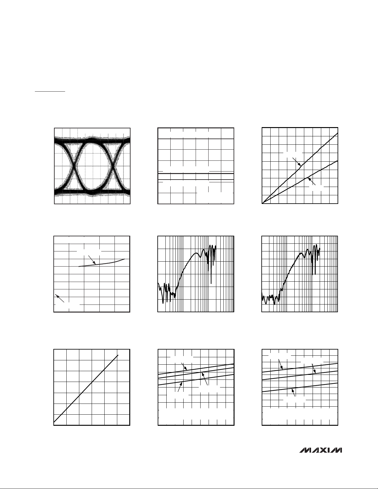
Typical Operating Characteristics—Limiting Amplifier
(VCC= 3.3V, TA= +25°C, unless otherwise specified. Figure 1 shows the typical setup used for measurements. Registers are set to
default values unless otherwise noted, and the 3-wire interface is static during measurements. For testing, the RATE_SEL bit was
used and the RSEL pin was left open.)
RANDOM JITTER
vs. INPUT AMPLITUDE
MAX3799 toc01
INPUT AMPLITUDE (mV
P-P
)
RANDOM JITTER (ps)
1000800600400200
310
320
330
340
350
360
370
300
0 1200
RATE_SEL = 1
DETERMINISTIC JITTER
vs. INPUT AMPLITUDE
MAX3799 toc03
INPUT AMPLITUDE (mV
P-P
)
DETERMINISTIC JITTER (ps)
1000800600400200
2
3
4
5
6
7
1
0 1200
PATTERN = PRBS, RATE_SEL = 1
AT 8.5Gbps
AT 10.32Gbps
OUTPUT EYE DIAGRAM AT 1.25Gbps
MAX3799 toc06
200ps/div
150mV/div
RATE_SEL = 0
OUTPUT EYE DIAGRAM AT 4.25Gbps
MAX3799 toc07
50ps/div
50mV/div
RATE_SEL = 1
OUTPUT EYE DIAGRAM AT 8.5Gbps
MAX3799 toc08
20ps/div
50mV/div
OUTPUT EYE DIAGRAM AT 10.32Gbps
MAX3799 toc09
20ps/div
50mV/div
DETERMINISTIC JITTER vs.
INPUT AMPLITUDE AT 1.25Gbps
25
PATTERN = k28.5, RATE_SEL = 0
23
21
19
17
15
13
11
9
DETERMINISTIC JITTER (ps)
7
5
3
0 1200
DETERMINISTIC JITTER
vs. DATA RATE
MAX3799 toc04
BER
1.0E-01
1.0E-02
1.0E-03
1.0E-04
1.0E-05
1.0E-06
1.0E-07
1.0E-08
1.0E-09
1.0E-10
1.0E-11
1.0E-12
1.0E-13
10
PATTERN = k28.5
9
8
7
6
5
DETERMINISTIC JITTER (ps)
4
3
2
014
RATE_SEL = 1
12102 4 6 8
DATA RATE (Gbps)
BER vs. INPUT AMPLITUDE
RATE_SEL = 0
0.5 3.0
INPUT AMPLITUDE (mV
RATE_SEL = 1
INPUT AMPLITUDE (mV
1000800600400200
)
P-P
2.52.01.0 1.5
)
P-P
MAX3799 toc02
MAX3799 toc05
Page 10
MAX3799
1Gbps to 14Gbps, SFP+ Multirate Limiting
Amplifier and VCSEL Driver
10 ______________________________________________________________________________________
Typical Operating Characteristics—Limiting Amplifier (continued)
(VCC= 3.3V, TA= +25°C, unless otherwise specified. Figure 1 shows the typical setup used for measurements. Registers are set to
default values unless otherwise noted, and the 3-wire interface is static during measurements. For testing, the RATE_SEL bit was
used and the RSEL pin was left open.)
LOS THRESHOLD vs. DAC SETTING
MAX3799 toc12
SET_LOS[5:0]
LOS THRESHOLD (mV)
564935 4214 21 287
20
40
60
80
100
120
140
160
180
0
063
DEASSERT
ASSERT
Rx INPUT RETURN LOSS
MAX3799 toc14
FREQUENCY (Hz)
SDD11 (dB)
10G1G
-50
-40
-30
-20
-10
0
-60
100M 100G
Rx OUTPUT RETURN LOSS
MAX3799 toc15
FREQUENCY (Hz)
SDD22 (dB)
10G1G
-45
-40
-35
-30
-25
-20
-15
-10
-5
0
-50
100M 100G
CML OUTPUT AMPLITUDE
vs. DAC SETTING
MAX3799 toc16
SET_CML[7:0]
CML OUTPUT AMPLITUDE (mV
P-P
)
25020015010050
200
400
600
800
1000
1200
1400
0
0 300
TOTAL SUPPLY CURRENT
vs. TEMPERATURE
MAX3799 toc17
TEMPERATURE (°C)
SUPPLY CURRENT (mA)
806535 50-10 5 20-25
50
60
70
80
90
100
110
120
130
140
40
-40 95
I
BIAS
= 12mA
I
BIAS
= 9mA
I
BIAS
= 2mA
I
MOD
= 2mA; RECEIVER OUTPUT = 400mV
P-P
;
TOTAL SUPPLY MEASURED USING THE SETUP
IN FIGURE 1
TOTAL SUPPLY CURRENT
vs. TEMPERATURE
MAX3799 toc18
TEMPERATURE (°C)
SUPPLY CURRENT (mA)
806535 50-10 5 20-25
50
60
70
80
90
100
110
120
130
140
150
160
40
-40 95
I
MOD
= 12mA
I
MOD
= 9mA
I
MOD
= 2mA
I
BIAS
= 2mA; RECEIVER OUTPUT = 400mV
P-P
;
TOTAL SUPPLY MEASURED USING THE SETUP
IN FIGURE 1
OUTPUT EYE DIAGRAM AT 14.025Gbps
RATE_SEL = 1, RXDE_EN = 1
MAX3799 toc10
70
60
50
TRANSITION TIME
vs. INPUT AMPLITUDE
RATE_SEL = 0, RXDE_EN = 0
MAX3799 toc11
50mV/div
-12
USING FINISAR ROSA
-13
-14
-15
-16
-17
-18
-19
SENSITIVITY OMA (dBm)
-20
-21
RATE_SEL = 0
-22
111
20ps/div
SENSITIVITY vs. DATA RATE
RATE_SEL = 1
9753
DATA RATE (Gbps)
TRANSITION TIME (ps)
MAAX3799 toc13
40
RATE_SEL = 1, RXDE_EN = 0
30
20
RATE_SEL = 1, RXDE_EN = 1
10
0
0 1200
INPUT AMPLITUDE (mV
PATTERN = 00001111
20% TO 80%
1000800600400200
)
P-P
Page 11
MAX3799
1Gbps to 14Gbps, SFP+ Multirate Limiting
Amplifier and VCSEL Driver
______________________________________________________________________________________
11
Typical Operating Characteristics—VCSEL Driver (continued)
(VCC= 3.3V, TA= +25°C, unless otherwise specified. Figure 1 shows the typical setup used for measurements. Registers are set to
default values unless otherwise noted, and the 3-wire interface is static during measurements. For testing, the RATE_SEL bit was
used and the RSEL pin was left open.)
OPTICAL EYE DIAGRAM
MAX3799 toc19
68ps/div
2.125Gbps, SET_IMOD = 60, 27 - 1 PRBS,
850nm VCSEL, MASK WITH 50%
OPTICAL EYE DIAGRAM
MAX3799 toc20
34ps/div
4.25Gbps, SET_IMOD = 60, 27 - 1 PRBS,
850nm VCSEL, MASK WITH 46%
OPTICAL EYE DIAGRAM
MAX3799 toc21
17ps/div
8.5Gbps, SET_IMOD = 60, 27 - 1 PRBS,
850nm VCSEL, MASK WITH 54%
OPTICAL EYE DIAGRAM
MAX3799 toc22
14ps/div
10.3Gbps, SET_IMOD = 60, 27 - 1 PRBS,
850nm VCSEL, MASK WITH 44%
DETERMINISTIC JITTER
vs. MODULATION CURRENT
MAX3799 toc24
MODULATION CURRENT (mA
P-P
)
DETERMINISTIC JITTER (ps)
10864
5.0
5.5
6.0
6.5
7.0
7.5
8.0
4.5
212
PATTERN = PRBS, DATA RATE = 10.32Gbps
TRANSITION TIME
vs. MODULATION CURRENT
MAX3799 toc25
MODULATION CURRENT (mA
P-P
)
TRANSITION TIME (ps)
10864
8
13
18
23
28
33
38
3
212
FALL TIME
RISE TIME
PATTERN = 11110000,
DATA RATE = 8.5Gbps
TRANSITION TIME
vs. DEEMPHASIS SETTING
MAX3799 toc26
SET_TXDE[3:0]
TRANSITION TIME (ps)
1091 2 3 5 6 74 8
27
29
31
33
35
37
39
41
25
011
FALL TIME
RISE TIME
PATTERN = 11110000,
DATA RATE = 8.5Gbps,
I
MOD
= 10mA
P-P
MODULATION CURRENT
vs. DAC SETTING
MAX3799 toc27
SET_IMOD[8:0]
MODULATION CURRENT (mA)
25020015010050
2
4
6
8
10
12
14
0
0 300
R
LOAD
= 50Ω
R
LOAD
= 75Ω
R
LOAD
= 100Ω
ELECTRICAL EYE DIAGRAM
14.025Gbps, SET_IMOD = 60, 231 - 1 PRBS
MAX3799 toc23
EYE WIDTH
62.8ps
14ps/div
Page 12

MAX3799
1Gbps to 14Gbps, SFP+ Multirate Limiting
Amplifier and VCSEL Driver
12 ______________________________________________________________________________________
Typical Operating Characteristics—VCSEL Driver (continued)
(VCC= 3.3V, TA= +25°C, unless otherwise specified. Figure 1 shows the typical setup used for measurements. Registers are set to
default values unless otherwise noted, and the 3-wire interface is static during measurements. For testing, the RATE_SEL bit was
used and the RSEL pin was left open.)
BIAS CURRENT
vs. DAC SETTING
MAX3799 toc28
SET_IBIAS[8:0]
BIAS CURRENT (mA)
25020015010050
2
4
6
8
10
12
14
0
0 300
TRANSMITTER DISABLE
MAX3799 toc29
100ns/div
V
CC
FAULT
DISABLE
OUTPUT
LOW
LOW
HIGH
3.3V
TRANSMITTER ENABLE
MAX3799 toc30
1μs/div
V
CC
FAULT
DISABLE
OUTPUT
LOW
LOW
HIGH
3.3V
tON = 420ns
RESPONSE TO FAULT
MAX3799 toc31
1μs/div
V
BIAS
FAULT
DISABLE
OUTPUT
LOW
LOW
HIGH
EXTERNALLY
FORCED FAULT
FAULT RECOVERY
MAX3799 toc32
4μs/div
V
BIAS
FAULT
DISABLE
OUTPUT
LOW
LOW
HIGH
EXTERNAL
FAULT
HIGH
FREQUENCY ASSERTION OF DISABLE
MAX3799 toc33
4μs/div
V
BIAS
FAULT
DISABLE
OUTPUT
LOW
LOW
HIGH
HIGH
EXTERNALLY
FORCED FAULT
Tx INPUT RETURN LOSS
MAX3799 toc34
FREQUENCY (Hz)
SDD11 (dB)
10G1G
-50
-40
-30
-20
-10
0
-60
100M 100G
Tx OUTPUT RETURN LOSS
MAX3799 toc35
FREQUENCY (Hz)
SDD22 (dB)
10G1G
-40
-35
-30
-25
-20
-15
-10
-5
0
-45
100M 100G
Page 13

MAX3799
1Gbps to 14Gbps, SFP+ Multirate Limiting
Amplifier and VCSEL Driver
______________________________________________________________________________________ 13
Pin Description
Typical Operating Characteristics—VCSEL Driver (continued)
(VCC= 3.3V, TA= +25°C, unless otherwise specified. Figure 1 shows the typical setup used for measurements. Registers are set to
default values unless otherwise noted, and the 3-wire interface is static during measurements. For testing, the RATE_SEL bit was
used and the RSEL pin was left open.)
DETERMINISTIC JITTER
vs. PULSE-WIDTH SETTING
MAX3799 toc36
SET_PWCTRL[3:0]
DETERMINISTIC JITTER (ps)
53-5 -3 -1 1
3
4
5
6
7
8
9
10
2
-7 7
PATTERN = PRBS, DATA RATE = 10.32Gbps
EYE CROSSING
DOWNUP
BIAS MONITOR CURRENT
vs. TEMPERATURE
MAX3799 toc37
TEMPERATURE (°C)
MONITOR CURRENT (μA)
8065-25 -10 5 3520 50
100
200
300
400
500
600
700
800
0
-40 95
I
BIAS
= 12mA
I
BIAS
= 8mA
I
BIAS
= 2mA
PIN NAME FUNCTION
Loss-of-Signal Output, Open Drain. The default polarity of LOS is high when the level of the input
1 LOS
signal is below the preset threshold set by the SET_LOS DAC. Polarity of the LOS function can be
inverted by sett ing LOS_POL = 0. The LOS circuitry can be disabled by setting the bit LOS_EN = 0.
2 RSEL
3, 6, 27, 30 V
4 ROUT+ Noninverted Receive Data Output, CML. Back-terminated for 50 load.
5 ROUT- In verted Receive Data Output, CML. Back-terminated for 50 load.
7 V
8 DISABLE
9 SCL Serial-Clock Input, TTL/CMOS. This pin has a 75k internal pul ldown.
10 SDA
11 CSEL
12, 15, 18,
21, 24, 25
13 TIN+ Noninverted Transmit Data Input, CML
Mode-Select Input, TTL/CMOS. Set the RSEL pin or RATE_SEL bit (set by the 3-wire digital interface)
to logic-high for high-bandwidth mode. Setting RSEL and RATE_SEL logic-low for high-gain mode.
The RSEL pin is internally pulled down by a 75k resistor to ground.
Power Supply. Provides supply voltage to the receiver block.
CCR
Power Supply. Provides supply voltage for the digital block.
CCD
Transm itter Disable Input, TTL/CMOS. Set to logic-low for normal operation. Logic-high or open
disables both the modulation and bias current. Internal ly pul led up by an 8k resistor to V
CCT
.
Serial-Data Bidirectional Input, TTL/CMOS. Open-drain output. This pin has a 75k internal pullup,
but it requires an external 4.7k pullup resistor to meet the 3-wire digital timing specification. (Data
line collision protection is implemented.)
Chip-Select Input, TTL/CMOS. Setting CSEL to logic-high starts a cycle. Setting CSEL to logic-low
ends the cycle and resets the control state machine. Internall y pulled down by a 75k resi stor to
ground.
V
Power Supply. Provides supply voltage to the transmitter block.
CCT
Page 14

MAX3799
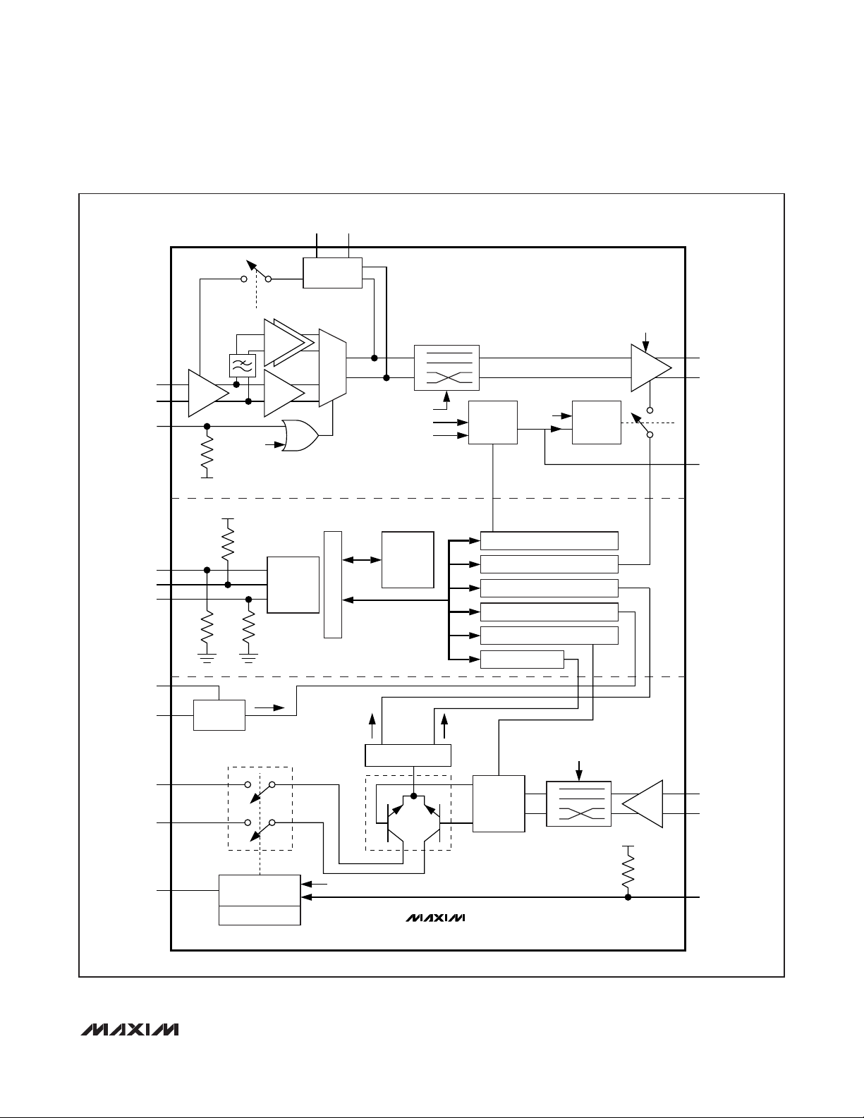
Detailed Description
The MAX3799 SFP+ transceiver combines a limiting
amplifier receiver with loss-of-signal detection and a
VCSEL laser driver transmitter with fault protection.
Configuration of the advanced Rx and Tx settings of the
MAX3799 is performed by a controller through the
3-wire interface. The MAX3799 provides multiple current and voltage DACs to allow the use of low-cost controller ICs.
Limiting Amplifier Receiver
The limiting amplifier receiver inside the MAX3799 is
designed to operate from 1.0625Gbps to 10.32Gbps.
The receiver includes a dual path limiter, offset correction circuitry, CML output stage with deemphasis, and
loss-of-signal circuitry. The functions of the receiver can
be controlled through the on-chip 3-wire interface. The
registers that control the receiver functionality are
RXCTRL1, RXCTRL2, RXSTAT, MODECTRL, SET_CML,
and SET_LOS.
1Gbps to 14Gbps, SFP+ Multirate Limiting
Amplifier and VCSEL Driver
14 ______________________________________________________________________________________
Pin Description (continued)
PIN NAME FUNCTION
14 TIN- Inverted Transmit Data Input, CML
16 BMON
17 V
19 TOUT- Inverted Modulation Current Output. Back-termination of 50 to V
20 TOUT+ Noninverted Modulation Current Output. Back-termination of 50 to V
22 BIAS VCSEL Bias Current Output
23 FAULT
26 V
28 RIN- Inverted Receive Data Input, CML
29 RIN+ Noninverted Receive Data Input, CML
31 CAZ2
32 CAZ1 Offset Correction Loop Capacitor. Counterpart to CAZ2, internally connected to V
— EP
EET
EER
Bias Current Mon itor Output. Current out of this pin develops a ground-referenced voltage across an
external resistor that is proportional to the laser bias current.
Ground. Provides ground for the tran sm itter block.
.
CCT
.
CCT
Transm itter Fault Output, Open Drain. Logic-high indicates a fault condition. FAULT remain s h igh
even after the fault condition has been removed. A logic-low occurs when the fault condition has
been removed and the fault latch has been cleared by the DISABLE signal.
Ground. Provides ground for the receiver b lock.
Offset Correction Loop Capacitor. A capacitor connected between this pin and CAZ1 sets the time
constant of the offset correction loop. The offset correction can be disabled through the digita l
interface by setting the bit AZ_EN = 0.
Exposed Pad. Ground. Must be soldered to circuit board ground for proper thermal and electrical
performance (see the Exposed-Pad Package section).
EER
.
Page 15
MAX3799
1Gbps to 14Gbps, SFP+ Multirate Limiting
Amplifier and VCSEL Driver
______________________________________________________________________________________ 15
Figure 2. Functional Diagram
CAZ2
CAZ1
RIN+
RIN-
RSEL
SCL
SDA
CSEL
900MHz
R
PULL
V
EER
R
PULLRPULL
AZ_EN
RATE_SEL
V
CCD
R
PULL
1G
3-WIRE
INTERFACE
OFFSET
CORRECTION
0
1
INTERNAL REGISTER
RX_POL
LOS_POL
LOS_EN
CONTROL
LOGIC
10.32Gbps LIMITING AMPLIFIER
RXDE_EN
1
0
SQ_EN
LOS
6b DAC SET_LOS
8b DAC SET_CML
9b DAC SET_IMOD
9b DAC SET_IBIAS
4b DAC SET_PWCTRL
4b DAC SET_TXDE
OUTPUT
CONTROL
LOGIC
ROUT+
ROUT-
LOS
BMON
BIAS
TOUT+
TOUT-
FAULT
BIAS
MONITOR
I
BIAS
EYE SAFETY AND
OUTPUT CONTROL
POWER-ON RESET
TX_EN
I
MOD
I
VCSEL
= I
MOD
MAX3799
I
DE
- I
DE
PULSE-
WIDTH
CONTROL
TX_POL
1
0
V
CCT
10.32Gbps VCSEL DRIVER
R
TIN+
TIN-
PULL
DISABLE
Page 16

MAX3799
1Gbps to 14Gbps, SFP+ Multirate Limiting
Amplifier and VCSEL Driver
16 ______________________________________________________________________________________
Dual Path Limiter
The limiting amplifier features a low data-rate mode
(1.25Gbps) and a high data-rate mode (up to
10.32Gbps), allowing for overall system optimization.
Either the RSEL pin or the RATE_SEL bit can perform
the rate selection. For operating up to 1.25Gbps, the
low data-rate mode (RATE_SEL = 0) is recommended.
For operation up to 14.025Gbps, the high data-rate
mode (RATE_SEL = 1) is recommended. The polarity of
the ROUT+/ROUT- relative to RIN+/RIN- is programmed by the RX_POL bit.
Offset Correction Circuitry
The offset correction circuit is enabled to remove pulsewidth distortion caused by intrinsic offset voltages within the differential amplifier stages. An external capacitor
(CAZ) connected between the CAZ1 and CAZ2 pins is
used to set the offset correction loop cutoff frequency.
The offset loop can be disabled using the AZ_EN bit.
CML Output Stage with Deemphasis
and Slew-Rate Control
The CML output stage is optimized for differential 100Ω
loads. The RXDE_EN bit adds analog deemphasis
compensation to the limited differential output signal for
SFP connector losses. The output stage is controlled by
a combination of the RX_EN and SQ_EN bits and the
LOS pin. See Table 1.
Amplitude of the CML output stage is controlled by an
8-bit DAC register (SET_CML). The differential output
amplitude range is from 40mV
P-P
up to 1200mV
P-P
with
4.6mV
P-P
resolution (assuming an ideal 100Ω differen-
tial load).
Loss-of-Signal (LOS) Circuitry
The input data amplitude is compared to a preset
threshold controlled by the 6-bit DAC register
SET_LOS. The LOS assert level can be programmed
from 14mV
P-P
up to 77mV
P-P
with 1.5mV
P-P
resolution
(assuming an ideal 100Ω differential source). LOS is
enabled through the LOS_EN bit and the polarity of the
LOS is controlled with the LOS_POL bit.
VCSEL Driver
The VCSEL driver inside the MAX3799 is designed to
operate from 1.0625Gbps to 10.32Gbps. The transmitter contains a differential data path with pulse-width
adjustment, bias current and modulation current DACs,
output driver with programmable deemphasis, poweron reset circuitry, BIAS monitor, VCSEL current limiter,
and eye safety circuitry. A 3-wire digital interface is
used to control the transmitter functions. The registers
that control the transmitter functionality are TXCTRL,
TXSTAT1, TXSTAT2, SET_IBIAS, SET_IMOD, IMODMAX, IBIASMAX, MODINC, BIASINC, MODECTRL,
SET_PWCTRL, and SET_TXDE.
Differential Data Path
The CML input buffer is optimized for AC-coupled signals and is internally terminated with a differential
100Ω. Differential input data is equalized for high-frequency losses due to SFP connectors. The TX_POL bit
in the TXCTRL register controls the polarity of TOUT+
and TOUT- vs. TIN+ and TIN-. The SET_PWCTRL register controls the output eye-crossing adjustment. A status indicator bit (TXED) monitors the presence of an AC
input signal.
Table 1. CML Output Stage Operation Mode
Table 2. Slew-Rate Control for CML
Output Stage
RX_EN SQ_EN LOS
0 X X CML output disabled.
1 0 X CML output enabled.
1 1 0 CML output enabled.
1 1 1 CML output disabled.
OPERATION MODE
DESCRIPTION
RATE_SEL OPERATION MODE DESCRIPTION
0
1 Up to 10.32Gbps operation.
1.25Gbps operation with reduced output
edge speed.
Page 17

Bias Current DAC
The bias current from the MAX3799 is optimized to provide up to 15mA of bias current into a 50Ω to 75Ω
VCSEL load with 40μA resolution. The bias current is
controlled through the 3-wire digital interface using the
SET_IBIAS, IBIASMAX, and BIASINC registers.
For VCSEL operation, the IBIASMAX register is first programmed to a desired maximum bias current value (up
to 15mA). The bias current to the VCSEL then can
range from zero to the value programmed into the
IBIASMAX register. The bias current level is stored in
the 9-bit SET_IBIAS register. Only bits 1 to 8 are written
to. The LSB (bit 0) of SET_IBIAS is initialized to zero
and is updated through the BIASINC register.
The value of the SET_IBIAS DAC register is updated
when the BIASINC register is addressed through the
3-wire interface. The BIASINC register is an 8-bit register where the first 5 bits contain the increment information in two’s complement notation. Increment values
range from -8 to +7 LSBs. If the updated value of
SET_IBIAS[8:1] exceeds IBIASMAX[7:0], the IBIASERR
warning flag is set and SET_IBIAS[8:0] remains
unchanged.
Modulation Current DAC
The modulation current from the MAX3799 is optimized
to provide up to 12mA of modulation current into a
100Ω differential load with 40μA resolution. The modulation current is controlled through the 3-wire digital
interface using the SET_IMOD, IMODMAX, MODINC,
and SET_TXDE registers.
For VCSEL operation, the IMODMAX register is first programmed to a desired maximum modulation current
value (up to 12mA into a 100Ω differential load). The
modulation current to the VCSEL then can range from
zero to the value programmed into the IMODMAX register. The modulation current level is stored in the 9-bit
SET_IMOD register. Only bits 1 to 8 are written to. The
LSB (bit 0) of SET_IMOD is initialized to zero and is
updated through the MODINC register.
The value of the SET_IMOD DAC register is updated
when the MODINC register is addressed through the
3-wire interface. The MODINC register is an 8-bit register where the first 5 bits contain the increment information in two’s complement notation. Increment values
range from -8 to +7 LSBs. If the updated value of
SET_IMOD[8:1] exceeds IMODMAX[7:0], the IMODERR
warning flag is set and SET_IMOD[8:0] remains
unchanged.
Output Driver
The output driver is optimized for an AC-coupled 100Ω
differential load. The output stage also features programmable deemphasis that allows the deemphasis amplitude to be set as a percentage of the modulation current.
The deemphasis function is enabled by the TXDE_EN
bit. At initial setup, the required amount of deemphasis
can be set using the SET_TXDE register. During the
system operation, it is advised to use the incremental
mode that updates the deemphasis (SET_TXDE) and
the modulation current DAC (SET_IMOD) simultaneously through the MODINC register.
Power-On Reset (POR)
Power-on reset ensures that the laser is off until the
supply voltage has reached a specified threshold
(2.55V). After power-on reset, bias current and modulation current ramp up slowly to avoid an overshoot. In
the case of a POR, all registers are reset to their default
values.
Bias Current Monitor
Current out of the BMON pin is typically 1/16th the
value of I
BIAS
. A resistor to ground at BMON sets the
voltage gain. An internal comparator latches a SOFT
FAULT if the voltage on BMON exceeds the value of
VCC- 0.55V.
Eye Safety and Output Control Circuitry
The safety and output control circuitry contains a disable pin (DISABLE) and disable bit (TX_EN), along with
a FAULT indicator and fault detectors (Figure 3). The
MAX3799 has two types of faults, HARD FAULT and
SOFT FAULT. A HARD FAULT triggers the FAULT pin
and the output to the VCSEL is disabled. A SOFT
FAULT operates more like a warning and the outputs
are not disabled. Both types of faults are stored in the
TXSTAT1 and TXSTAT2 registers.
The FAULT pin is a latched output that can be cleared
by toggling the DISABLE pin. Toggling the DISABLE
pin also clears the TXSTAT1 and TXSTAT2 registers. A
single-point fault can be a short to V
CC
or GND. Table
3 shows the circuit response to various single-point
failures.
MAX3799
1Gbps to 14Gbps, SFP+ Multirate Limiting
Amplifier and VCSEL Driver
______________________________________________________________________________________ 17
Page 18

MAX3799
1Gbps to 14Gbps, SFP+ Multirate Limiting
Amplifier and VCSEL Driver
18 ______________________________________________________________________________________
Figure 3. Eye Safety Circuitry
BIAS
I
BIAS
I
BIAS
16
I
MOD
V
CCT
FAULT REGISTER TXSTAT1
0.72V
0.8V
1.5V
<0>
FAULT
<1>
<2>
<3>
FAULT REGISTER
TXSTAT1
<4>
TOUT-
TOUT+
<5>
BMON
V
CCT
DISABLE
8kΩ
POR
LOSS-OF-SIGNAL
CIRCUIT
VCC - 0.55V
POR
TX_LOS
BIAS INCREMENT
BIASMAX
MOD INCREMENT
MODMAX
<6>
<7>
RESET
WARNING REGISTER
TXSTAT2
<0>UNUSED
ADDR7
<1>
<2>
<3>
Page 19

MAX3799
1Gbps to 14Gbps, SFP+ Multirate Limiting
Amplifier and VCSEL Driver
______________________________________________________________________________________ 19
Table 3. Circuit Response to Single-Point Faults
PIN NAME SHORT TO VCC SHORT TO GND OPEN
1 LOS Normal (Note 1) Normal (Note 1) Normal (Note 1)
2 RSEL Normal (Note 1) Normal (Note 1) Normal (Note 1)
3 V
4 ROUT+ Normal (Note 1) Normal (Note 1) Normal (Note 1)
5 ROUT- Normal (Note 1) Normal (Note 1) Normal (Note 1)
6 V
7 V
8 DISABLE Disabled
9 SCL Normal (Note 1) Normal (Note 1) Normal (Note 1)
10 SDA Normal (Note 1) Normal (Note 1) Normal (Note 1)
11 CSEL Normal (Note 1) Normal (Note 1) Normal (Note 1)
12 V
13 TIN+ SOFT FAULT SOFT FAULT Normal (Note 1)
14 TIN- SOFT FAULT SOFT FAULT Normal (Note 1)
15 V
16 BMON Disabled—HARD FAULT Normal (Note 1) Disabled—HARD FAULT
17 V
18 V
19 TOUT- I
20 TOUT+ I
21 V
22 BIAS I
23 FAULT Normal (Note 1) Normal (Note 1) Normal (Note 1)
24 V
25 V
26 V
27 V
28 RIN- Normal (Note 1) Normal (Note 1) Normal (Note 1)
29 RIN+ Normal (Note 1) Normal (Note 1) Normal (Note 1)
Normal
CCR
Normal
CCR
Normal Disabled—HARD FAULT Disabled—HARD FAULT
CCD
Normal
CCT
Normal
CCT
Disabled—Fault (external supply
EET
shorted) (Note 2)
Normal
CCT
is reduced Disabled—HARD FAULT I
MOD
is reduced Disabled—HARD FAULT I
MOD
Normal
CCT
is on—No Fault Disabled—HARD FAULT Disabled—HARD FAULT
BIAS
Normal
CCT
Normal
CCT
Disabled—Fault (external supply
EER
shorted) (Note 2)
Normal
CCR
Disabled—HARD FAULT (external
supply shorted) (Note 2)
Disabled—HARD FAULT (external
supply shorted) (Note 2)
Normal (Note 1). Can only be
disabled with other mean s.
Disabled—Fault (external supply
shorted) (Note 2)
Disabled—Fault (external supply
shorted) (Note 2)
Normal Disabled—HARD FAULT
Disabled—Fault (external supply
shorted) (Note 2)
Disabled—Fault (external supply
shorted) (Note 2)
Disabled—Fault (external supply
shorted) (Note 2)
Disabled—Fault (external supply
shorted) (Note 2)
Normal Normal (Note 3)—Redundant path
Disabled—HARD FAULT (external
supply shorted) (Note 2)
Normal (Note 3)—Redundant path
Normal (Note 3)—Redundant path
Disabled
Normal (Note 3)—Redundant path
Normal (Note 3)—Redundant path
Normal (Note 3)—Redundant path
is reduced
MOD
is reduced
MOD
Normal (Note 3)—Redundant path
Normal (Note 3)—Redundant path
Normal (Note 3)—Redundant path
Normal (Note 3)—Redundant path
Page 20

MAX3799
3-Wire Digital Communication
The MAX3799 implements a proprietary 3-wire digital
interface. An external controller generates the clock. The
3-wire interface consists of an SDA bidirectional data
line, an SCL clock signal input, and a CSEL chip-select
input (active high). The external master initiates a data
transfer by asserting the CSEL pin. The master starts to
generate a clock signal after the CSEL pin has been set
to 1. All data transfers are most significant bit (MSB) first.
Protocol
Each operation consists of 16-bit transfers (15-bit
address/data, 1-bit RWN). The bus master generates
16 clock cycles to SCL. All operations transfer 8 bits to
the MAX3799. The RWN bit determines if the cycle is
read or write. See Table 4.
Register Addresses
The MAX3799 contains 17 registers available for programming. Table 5 shows the registers and addresses.
Write Mode (RWN = 0)
The master generates 16 clock cycles at SCL in total.
The master outputs a total of 16 bits (MSB first) to the
SDA line at the falling edge of the clock. The master
closes the transmission by setting CSEL to 0. Figure 4
shows the interface timing.
Read Mode (RWN = 1)
The master generates 16 clock cycles at SCL in total.
The master outputs a total of 8 bits (MSB first) to the
SDA line at the falling edge of the clock. The SDA line is
released after the RWN bit has been transmitted. The
slave outputs 8 bits of data (MSB first) at the rising edge
of the clock. The master closes the transmission by setting CSEL to 0. Figure 4 shows the interface timing.
Mode Control
Normal mode allows read-only instruction for all registers except MODINC and BIASINC. The MODINC and
BIASINC registers can be updated during normal
mode. Doing so speeds up the laser control update
through the 3-wire interface by a factor of two. The normal mode is the default mode.
Setup mode allows the master to write unrestricted data
into any register except the status (TXSTAT1, TXSTAT2,
and RXSTAT) registers. To enter the setup mode, the
MODECTRL register (address = H0x0E) must be set to
H0x12. After the MODECTRL register has been set to
H0x12, the next operation is unrestricted. The setup
mode is automatically exited after the next operation is
finished. This sequence must be repeated if further
unrestricted settings are necessary.
1Gbps to 14Gbps, SFP+ Multirate Limiting
Amplifier and VCSEL Driver
20 ______________________________________________________________________________________
Table 3. Circuit Response to Single-Point Faults (continued)
Table 4. Digital Communication Word Structure
Note 1: Normal—Does not affect laser power.
Note 2: Supply-shorted current is assumed to be primarily on the circuit board (outside this device) and the main supply is
collapsed by the short.
Note 3: Normal in functionality, but performance could be affected.
Warning: Shorted to V
CC
or shorted to ground on some pins can violate the
Absolute Maximum Ratings
.
PIN NAME SHORT TO VCC SHORT TO GND OPEN
30 V
31 CAZ2 Normal (Note 1) Normal (Note 1) Normal (Note 1)
32
Normal
CCR
CAZ1
)
(V
EER
Disabled—Fault (external supply
shorted) (Note 2)
Disabled—Fault (external supply
shorted) (Note 2)
Normal (Note 3)—Redundant path Normal (Note 3)—Redundant path
Normal (Note 3)—Redundant path
BIT
15 14 13 12 11 10 9 8 7 6 5 4 3 2 1 0
Regi ster Address RWN Data that is written or read.
Page 21

MAX3799
1Gbps to 14Gbps, SFP+ Multirate Limiting
Amplifier and VCSEL Driver
______________________________________________________________________________________ 21
Table 5. Register Descriptions and Addresses
CSEL
SCL
SDA
CSEL
SCL
SDA
12345678A69 1011121314150
1234567891011121314150
A5 A4 A3 A2 A1 RWN D7 D6 D5 D4 D3 D2 D1 D0
D7 D6 D5 D4 D3 D2 D1 D0RWN
WRITE MODE
READ MODE
A0
A6 A5 A4 A3 A2 A1 A0
t
L
t
L
tCHt
CL
t
DS
t
DH
tCHt
CL
t
DS
t
D
t
DH
t
T
t
T
Figure 4. Timing for 3-Wire Digital Interface
ADDRESS NAME FUNCTION
H0x00 RXCTRL1 Receiver Control Register 1
H0x01 RXCTRL2 Receiver Control Register 2
H0x02 RXSTAT Receiver Status Register
H0x03 SET_CML Output CML Level Setting Register
H0x04 SET_LOS LOS Threshold Le ve l Sett ing Register
H0x05 TXCTRL Transmitter Control Register
H0x06 TXSTAT1 Transmitter Status Register 1
H0x07 TXSTAT2 Transmitter Status Register 2
H0x08 SET_IBIAS Bias Current Setting Register
H0x09 SET_IMOD Modulation Current Setting Register
H0x0A IMODMAX Maximum Modulation Current Setting Register
H0x0B IBIASMAX Maximum Bias Current Setting Register
H0x0C MODINC Modulation Current Increment Setting Regi ster
H0x0D BIASINC Bias Current Increment Setting Register
H0x0E MODECTRL Mode Control Register
H0x0F SET_PWCTRL Transmitter Pulse-Width Control Register
H0x10 SET_TXDE Transmitter Deempha si s Control Register
Page 22
MAX3799
Register Descriptions
Receiver Control Register 1 (RXCTRL1)
Bit 1: RATE_SEL. RATE_SEL combined with the RSEL pin through a logic-OR function selects between the low
data-rate mode (1.25Gbps) or high data-rate mode (up to 10.32Gbps).
Logic-OR output 0 = 1Gbps mode
Logic-OR output 1 = 10Gbps mode
Receiver Control Register 2 (RXCTRL2)
Bit 6: LOS_EN. Controls the LOS circuitry. When RX_EN is set to 0, the LOS detector is also disabled.
0 = disabled
1 = enabled
Bit 5: LOS_POL. Controls the output polarity of the LOS pin.
0 = inverse
1 = normal
Bit 4: RX_POL. Controls the polarity of the receiver signal path.
0 = inverse
1 = normal
Bit 3: SQ_EN. When SQ_EN = 1, the LOS controls the output circuitry.
0 = disabled
1 = enabled
Bit 2: RX_EN. Enables or disables the receive circuitry.
0 = disabled
1 = enabled
Bit 1: RXDE_EN. Enables or disables the deemphasis on the receiver output.
0 = disabled
1 = enabled
Bit 0: AZ_EN. Enables or disables the autozero circuitry. When RX_EN is set to 0, the autozero circuitry is also disabled.
0 = disabled
1 = enabled
1Gbps to 14Gbps, SFP+ Multirate Limiting
Amplifier and VCSEL Driver
22 ______________________________________________________________________________________
Bit # 7 6 5 4 3 2 1 0 ADDRESS
Name X X X X X X RATE_SEL X
Default Value X X X X X X 0 X
Bit # 7 6 5 4 3 2 1 0 ADDRESS
Name X LOS_EN LOS_POL RX_POL SQ_EN RX_EN RXDE_EN AZ_EN
Default Value X 1 1 1 0 1 0 1
H0x00
H0x01
Page 23

MAX3799
1Gbps to 14Gbps, SFP+ Multirate Limiting
Amplifier and VCSEL Driver
______________________________________________________________________________________ 23
Receiver Status Register (RXSTAT)
Bit 0: LOS. Copy of the LOS output circuitry. This is a sticky bit, which means that it is cleared on a read. The first
0-to-1 transition gets latched until the bit is read by the master or POR occurs.
Output CML Level Setting Register (SET_CML)
Bits 7 to 0: SET_CML[7:0]. The SET_CML register is an 8-bit register that can be set up to 255, corresponding to an
output up to 1000mV
P-P
. See the
Typical Operating Characteristics
section for a typical CML output voltage vs. DAC
code graph.
LOS Threshold Level Setting Register (SET_LOS)
Bits 5 to 0: SET_LOS[5:0]. The SET_LOS register is a 6-bit register used to program the LOS threshold. See the
Typical Operating Characteristics
section for a typical LOS threshold voltage vs. DAC code graph.
Bit # 7 6 5 4 3 2 1
Name X X X X X X X LOS
Default Value X X X X X X X X
0
(STICKY)
ADDRESS
H0x02
Bit # 7 6 5 4 3 2 1 0 ADDRESS
Name
Default Value 0 1 0 1 0 0 1 1
SET_CML[7]
(MSB)
SET_CML[6] SET_CML[5] SET_CML[4] SET_CML[3] SET_CML[2] SET_CML[1]
SET_CML[0]
(LSB)
H0x03
Bit # 7 6 5 4 3 2 1 0 ADDRESS
Name X X
Default Value X X 0 0 1 1 0 0
SET_LOS[5]
(MSB)
SET_LOS[4] SET_LOS[3] SET_LOS[2] SET_LOS[1]
SET_LOS[0]
(LSB)
H0x04
Page 24

MAX3799
Transmitter Control Register (TXCTRL)
Bit 3: TXDE_EN. Enables or disables the transmit output deemphasis circuitry.
0 = disabled
1 = enabled
Bit 2: SOFTRES. Resets all registers to their default values.
0 = normal
1 = reset
Bit 1: TX_POL. Controls the polarity of the transmit signal path.
0 = inverse
1 = normal
Bit 0: TX_EN. Enables or disables the transmit circuitry.
0 = disabled
1 = enabled
Transmitter Status Register 1 (TXSTAT1)
Bit 7: FST[7]. When the V
CCT
supply voltage is below 2.45V, the POR circuitry reports a FAULT. Once the V
CCT
supply voltage is above 2.55V, the POR resets all registers to their default values and the FAULT is cleared.
Bit 6: FST[6]. When the voltage at BMON is above VCC- 0.55V, a SOFT FAULT is reported.
Bit 3: FST[3]. When the common-mode voltage at V
TOUT
+/- goes below 1.5V, a SOFT FAULT is reported.
Bit 2: FST[2]. When the voltage at V
TOUT
+/- goes below 0.8V, a HARD FAULT is reported.
Bit 1: FST[1]. When the BIAS voltage goes below 0.44V, a HARD FAULT is reported.
Bit 0: TX_FAULT. Copy of a FAULT signal in FST[7] to FST[1]. A POR resets FST[7:1] to 0.
Transmitter Status Register 2 (TXSTAT2)
Bit 3: IMODERR. When the modulation-incremented result is greater than IMODMAX, a SOFT FAULT is reported.
See the
Programming Modulation Current
section.
1Gbps to 14Gbps, SFP+ Multirate Limiting
Amplifier and VCSEL Driver
24 ______________________________________________________________________________________
Bit # 7 6 5 4 3 2 1 0 ADDRESS
Name X X X X TXDE_EN SOFTRES TX_POL TX_EN
Default Value X X X X 0 0 1 1
H0x05
Bit #
Nam e FST[7] FST[6] X X FST[3] FST[2] FST[1] TX_F AU LT
Default Value X X X X X X X X
7
(STICKY) 6(STICKY) 5(STICKY) 4(STICKY) 3(STICKY) 2(STICKY) 1(STICKY) 0(STICKY)
ADDRESS
H0x06
Bit # 7 6 5 4
Name X X X X IMODERR IBIASERR TXED X
Default Value X X X X X X X X
3
(STICKY) 2(STICKY) 1(STICKY) 0(STICKY)
ADDRESS
H0x07
Page 25

Bit 2: IBIASERR. When the bias incremented result is greater than IBIASMAX, then a SOFT FAULT is reported. See
the
Programming Bias Current
section.
Bit 1: TXED. This only indicates the absence of an AC signal at the transmit input. This is not an LOS indicator.
Bias Current Setting Register (SET_IBIAS)
Bits 7 to 0: SET_IBIAS[8:1]. The bias current DAC is controlled by a total of 9 bits. The SET_IBIAS[8:1] bits are
used to set the bias current with even denominations from 0 to 510 bits. The LSB (SET_IBIAS[0]) bit is controlled by
the BIASINC register and is used to set the odd denominations in the SET_IBIAS[8:0].
Modulation Current Setting Register (SET_IMOD)
Bits 7 to 0: SET_IMOD[8:1]. The modulation current DAC is controlled by a total of 9 bits. The SET_IMOD[8:1] bits
are used to set the modulation current with even denominations from 0 to 510 bits. The LSB (SET_IMOD[0]) bit is
controlled by the MODINC register and is used to set the odd denominations in the SET_IMOD[8:0].
Maximum Modulation Current Setting Register (IMODMAX)
Bits 7 to 0: IMODMAX[7:0]. The IMODMAX register is an 8-bit register that can be used to limit the maximum modu-
lation current. IMODMAX[7:0] is continuously compared to the SET_IMOD[8:1].
Maximum Bias Current Setting Register (IBIASMAX)
Bits 7 to 0: IBIASMAX[7:0]. The IBIASMAX register is an 8-bit register that can be used to limit the maximum bias
current. IBIASMAX[7:0] is continuously compared to the SET_IBAS[8:1].
MAX3799
1Gbps to 14Gbps, SFP+ Multirate Limiting
Amplifier and VCSEL Driver
______________________________________________________________________________________ 25
Bit # 7 6 5 4 3 2 1 0 ADDRES S
Name
Default Value 0 0 0 0 0 1 0 0
SET_IBIAS
[8] (MSB)
SET_IBIAS
[7]
SET_IBIAS
[6]
SET_IBIAS
[5]
SET_IBIAS
[4]
SET_IBIAS
[3]
SET_IBIAS
[2]
SET_IBIAS
[1]
H0x08
Bit # 7 6 5 4 3 2 1 0 ADDRES S
Name
Default Value 0 0 0 1 0 0 1 0
SET_IMOD
[8] (MSB)
SET_IMOD
[7]
SET_IMOD
[6]
SET_IMOD
[5]
SET_IMOD
[4]
SET_IMOD
[3]
SET_IMOD
[2]
SET_IMOD
[1]
H0x09
Bit # 7 6 5 4 3 2 1 0 ADDRES S
Name
Default Value 0 0 1 1 0 0 0 0
IMODMAX
[7] (MSB)
IMODMAX
[6]
IMODMAX
[5]
IMODMAX
[4]
IMODMAX
[3]
IMODMAX
[2]
IMODMAX
[1]
IMODMAX
[0] (LSB)
H0x0A
Bit # 7 6 5 4 3 2 1 0 ADDRES S
Name
Default Value 0 0 0 1 0 0 1 0
IBIASMAX
[7] (MSB)
IBIASMAX
[6]
IBIASMAX
[5]
IBIASMAX
[4]
IBIASMAX
[3]
IBIASMAX
[2]
IBIASMAX
[1]
IBIASMAX
[0] (LSB)
H0x0B
Page 26

MAX3799
Modulation Current Increment Setting Register (MODINC)
Bit 7: SET_IMOD[0]. This is the LSB of the SET_IMOD[8:0] bits. This bit can only be updated by the use of
MODINC[4:0].
Bit 5: DE_INC. When this bit is set to 1 and the deemphasis on the transmit output is enabled, the SET_TXDE[3:0] is
incremented or decremented by 1 LSB. The increment or decrement is determined by the sign bit of the MODINC[4:0]
string of bits.
Bits 4 to 0: MODINC[4:0]. This string of bits is used to increment or decrement the modulation current. When written
to, the SET_IMOD[8:0] bits are updated. MODINC[4:0] are a two’s complement string.
Bias Current Increment Setting Register (BIASINC)
Bit 7: SET_IBIAS[0]. This is the LSB of the SET_IBIAS[8:0] bits. This bit can only be updated by the use of BIASINC[4:0].
Bits 4 to 0: BIASINC[4:0]. This string of bits is used to increment or decrement the bias current. When written to, the
SET_IBIAS[8:0] bits are updated. BIASINC[4:0] are a two’s complement string.
Mode Control Register (MODECTRL)
Bits 7 to 0: MODECTRL[7:0]. The MODECTRL register enables a switch between normal and setup modes. The
setup mode is achieved by setting this register to H0x12. MODECTRL must be updated before each write operation.
Exceptions are MODINC and BIASINC, which can be updated in normal mode.
Transmitter Pulse-Width Control Register (SET_PWCTRL)
Bits 3 to 0: SET_PWCTRL[3:0]. This is a 4-bit register used to control the eye crossing by adjusting the pulse width.
1Gbps to 14Gbps, SFP+ Multirate Limiting
Amplifier and VCSEL Driver
26 ______________________________________________________________________________________
Bit # 7 6 5 4 3 2 1 0 ADDRES S
Name
Default Value 0 0 0 0 0 0 0 0
SET_IMOD
[0]
X DE_INC
MODINC[4]
(MSB)
MODINC[3] MODINC[2] MODINC[1]
Bit # 7 6 5 4 3 2 1 0 ADDRES S
Name
Default Value 0 0 0 0 0 0 0 0
SET_IBIAS
[0]
X X
BIASINC[4]
(MSB)
BIASINC[3] BIASINC[2] BIASINC[1]
MODINC[0]
(LSB)
BIASINC[0]
(LSB)
H0x0C
H0x0D
Bit # 7 6 5 4 3 2 1 0 ADDRES S
Name
Default Value 0 0 0 0 0 0 0 0
MODECTRL
[7] (MSB)
MODECTRL
[6]
MODECTRL
[5]
MODECTRL
[4]
MODECTRL
[3]
MODECTRL
[2]
MODECTRL
[1]
MODECTRL
[0] (LSB)
H0x0E
Bit # 7 6 5 4 3 2 1 0 ADDRES S
SET_
Name X X X X
Default Value X X X X 0 0 0 0
PWCTRL[3]
(MSB)
SET_
PWCTRL[2]
SET_
PWCTRL[1]
SET_
PWCTRL[0]
(LSB)
H0x0F
Page 27

Design Procedure
Programming Bias Current
1) IBIASMAX[7:0] = Maximum_Bias_Current_Value
2) SET_IBIASi[8:1] = Initial_Bias_Current_Value
Note: The total bias current value is calculated using
the SET_IBIAS[8:0] register. SET_IBIAS[8:1] are the bits
that can be manually written. SET_IBIAS[0] can only be
updated using the BIASINC[4:0] register.
When implementing an APC loop, it is recommended to
use the BIASINC[4:0] register, which guarantees the
fastest bias current update.
3) BIASINCi[4:0] = New_Increment_Value
4) If (SET_IBIASi[8:1] ≤ IBIASMAX[7:0]),
then (SET_IBIASi[8:0] = SET_IBIAS
i-1
[8:0] + BIASINCi[4:0])
5) Else (SET_IBIASi[8:0] = SET_IBIAS
i-1
[8:0])
The total bias current can be calculated as follows:
6) I
BIAS
= [SET_IBIASi[8:0] + 20] x 40μA
Programming Modulation Current
1) IMODMAX[7:0] = Maximum_Modulation_Current_Value
2) SET_IMODi[8:1] = Initial_Modulation_Current_Value
Note: The total modulation current value is calculated
using the SET_IMOD[8:0] register. SET_IMOD[8:1] are
the bits that can be manually written. SET_IMOD[0] can
only be updated using the MODINC[4:0] register.
When implementing modulation compensation, it is recommended to use the MODINC[4:0] register, which
guarantees the fastest modulation current update.
3) MODINC
i
[4:0] = New_Increment_Value
4) If (SET_IMODi[8:1] ≤ IMODMAX[7:0]),
then (SET_IMODi[8:0] = SET_IMOD
i-1
[8:0] + MODINCi[4:0])
5) Else (SET_IMOD
i
[8:0] = SET_IMOD
i-1
[8:0])
The following equation is valid with assumption of 100Ω
on-chip and 100Ω external differential load (Rextd). The
maximum value that can be set for SET_TXDE[3:0] = 11.
6) I
MOD(Rextd=100Ω)
= [(20 + SET_IMODi[8:0]) x 40μA]
For general Rextd, the modulation current that is
achieved using the same setting of SET_IMODi[8:0] as
for Rextd = 100Ω is shown below. It can be written as a
function of I
MOD(Rextd=100Ω)
, still assuming a 100Ω on-
chip load.
7)
Programming LOS Threshold
LOSTH= (SET_LOS[5:0] x 1.5mV
P-P
)
Programming Transmit Output
Deemphasis
The TXDE_EN bit must be set to 1 to enable the deemphasis function. The SET_TXDE register value is used
to set the amount of deemphasis, which is a percentage of the modulation current. Deemphasis percentage
is determined as:
where the maximum SET_TXDE[3:0] = 11.
For an I
MOD
value of 10mA, the maximum achievable
deemphasis value is approximately 20%. Maximum
deemphasis achievable for full I
MOD
range of 12mA is
limited to 15%.
With deemphasis enabled, the value of the modulation
current amplitude is reduced by the calculated deemphasis percentage. To maintain the modulation current
amplitude constant, the SET_IMOD[8:0] register must
be increased by the deemphasis percentage. If the system conditions like temperature, required I
MOD
value,
etc., change during the transmit operation, the deemphasis setting might need to be readjusted. For such an
Transmitter Deemphasis Control Register (SET_TXDE)
Bits 3 to 0: SET_TXDE[3:0]. This is a 4-bit register used to control the amount of deemphasis on the transmitter out-
put. When calculating the total modulation current, the amount of deemphasis must be taken into account. The
deemphasis is set as a percentage of modulation current.
MAX3799
1Gbps to 14Gbps, SFP+ Multirate Limiting
Amplifier and VCSEL Driver
______________________________________________________________________________________ 27
Bit # 7 6 5 4 3 2 1 0 ADDRES S
Name X X X X
Default Value X X X X 0 0 0 0
SET_TXDE
[3] (MSB)
II
MOD xt d MOD xtd(Re ) (Re )
SET_TXDE
[2]
×−
SET_TXDE
[1]
+
230
⎡
1
⎢
⎣
2
=×
_[:]
SET TXDE
64
SET TXDE
×+
100 2 3 0
DE
(%)
=
()
SET_TXDE
[0] (LSB)
⎤
⎥
⎦
Re
100
⎡
⎢
⎣⎣
Re
xt
=Ω
_[:]
64
H0x10
+
xt
100
⎤
⎥
⎦
Page 28

MAX3799
impromptu deemphasis adjustment, it is recommended
that the DE_INC (MODINC[5]) bit is used. Use of this bit
increments or decrements the deemphasis code setting
by 1 LSB based on the sign of increment in the
MODINC[4:0] and, hence, the SET_IMOD[8:0] setting.
This helps maintain the BER while having the flexibility to
improve signal quality by adjusting deemphasis while
the transmit operation continues. This feature enables
glitchless deemphasis adjustment while maintaining
excellent BER performance.
Activating Receiver Output Deemphasis
The RXDE_EN bit must be set to 1 to enable the deemphasis function. Deemphasis decreases the output
amplitude at ROUT+/ROUT- by 25%. To maintain the
same output amplitude as before the activation of
deemphasis, the SET_CML register value needs to be
increased by 25%. When deemphasis is enabled, the
limiting amplifier AC performance is guaranteed up to
800mV
P-P
typical output amplitude. The SET_CML register can be set from 0 to 255 bits, but it is important to
note that performance is guaranteed up to 215 bits.
Programming Pulse-Width Control
The eye crossing at the Tx output can be adjusted using
the SET_PWCTRL register. Table 6 shows these settings.
The sign of the number specifies the direction of pulsewidth distortion. The code of 1111 corresponds to a
balanced state for differential output. The pulse-width
distortion is bidirectional around the balanced state
(see the
Typical Operating Characteristics
section).
Programming CML Output Settings
Amplitude of the CML output stage is controlled by an
8-bit DAC register (SET_CML). The differential output
amplitude is up to 1000mV
P-P
with 4.6mV
P-P
resolution
(assuming an ideal 100Ω differential load). The guaranteed output CML DAC range is up to 215.
Output Voltage R
OUT
(mV
P-P
) = 40 + 4.55 (SET_CML)
Select the Coupling Capacitor
For AC-coupling, the coupling capacitors CINand
C
OUT
should be selected to minimize the receiver’s
deterministic jitter. Jitter is decreased as the input lowfrequency cutoff (fIN) is decreased.
fIN= 1/[2π(50)(CIN)]
The recommended CINand C
OUT
is 0.1μF for the
MAX3799.
Select the Offset-Correction Capacitor
The capacitor between CAZ1 and CAZ2 determines the
time constant of the signal path DC-offset cancellation
loop. To maintain stability, it is important to keep at
least a one-decade separation between fINand the
low-frequency cutoff (fOC) associated with the DC-offset cancellation circuit. A 1nF capacitor between CAZ1
and CAZ2 is recommended for the MAX3799.
Applications Information
Layout Considerations
To minimize inductance, keep the connections between
the MAX3799 output pins and laser diode as close as
possible. Optimize the laser diode performance by
placing a bypass capacitor as close as possible to the
laser anode. Use good high-frequency layout techniques and multiple-layer boards with uninterrupted
ground planes to minimize EMI and crosstalk.
Exposed-Pad Package
The exposed pad on the 32-pin TQFN provides a very
low-thermal resistance path for heat removal from the IC.
The pad is also electrical ground on the MAX3799 and
must be soldered to the circuit board ground for proper
thermal and electrical performance. Refer to Application
Note 862:
HFAN-08.1: Thermal Considerations of QFN
and Other Exposed-Paddle Packages
for additional
information.
Laser Safety and IEC 825
Using the MAX3799 laser driver alone does not ensure
that a transmitter design is compliant with IEC 825. The
entire transmitter circuit and component selections
must be considered. Each user must determine the
level of fault tolerance required by the application, recognizing that Maxim products are neither designed nor
authorized for use as components in systems intended
for surgical implant into the body, for applications
intended to support or sustain life, or for any other
application in which the failure of a Maxim product
could create a situation where personal injury or death
could occur.
1Gbps to 14Gbps, SFP+ Multirate Limiting
Amplifier and VCSEL Driver
28 ______________________________________________________________________________________
Table 6. Eye-Crossing Settings for
SET_PWCTRL
SET_PWCTRL[3:0] PWD SET_PWCTRL[3:0] PWD
1000 -7 0111 8
1001 -6 0110 7
1010 -5 0101 6
1011 -4 0100 5
1100 -3 0011 4
1101 -2 0010 3
1110 -1 0001 2
1111 0 0000 1
Page 29

MAX3799
1Gbps to 14Gbps, SFP+ Multirate Limiting
Amplifier and VCSEL Driver
______________________________________________________________________________________ 29
Table 7. Register Summary
REGISTER
FUNCTION/
ADDRESS
Receiver Control
Regi ster 1
Address = H0x00
Receiver Control
Regi ster 2
Address = H0x01
Receiver Status
Register
Address = H0x02
Output CML Level
Setting Register
Address = H0x03
LOS Threshold
Level Setting
Register
Address = H0x04
REGISTER
NAME
RXCTRL1 R RW 1 R ATE_SEL 0
RXCTRL2
RXSTAT R R 0 (sticky) LOS X Copy of LOS output signal
SET_CML
SET_LOS
NORMAL
SETUP
MODE
R RW 6 LOS_EN 1
R RW 5 LOS_POL 1
R RW 4 RX_POL 1
R RW 3 SQ_EN 0
R RW 2 RX_EN 1
R RW 1 RXDE_EN 0
R RW 0 AZ_EN 1
R RW 7 SET_CML[7] 0 MSB output leve l DAC
R RW 6 SET_CML[6] 1
R RW 5 SET_CML[5] 0
R RW 4 SET_CML[4] 1
R RW 3 SET_CML[3] 0
R RW 2 SET_CML[2] 0
R RW 1 SET_CML[1] 1
R RW 0 SET_CML[0] 1 LSB output level DAC
R RW 5 SET_LOS[5] 0 MSB LOS thresho ld DAC
R RW 4 SET_LOS[4] 0
R RW 3 SET_LOS[3] 1
R RW 2 SET_LOS[2] 1
R RW 1 SET_LOS[1] 0
R RW 0 SET_LOS[0] 0 LSB LOS threshold DAC
MODE
BIT
NUMBER
/TYPE
BIT NAME
DEFAULT
VALUE
NOTES
Mode-select
0: high-gain mode, 1: highbandwidth mode
LOS control
0: disable, 1: enable
(always 0 when RX_EN = 0)
LOS polarity
0: inverse, 1: normal
Rx polarity
0: inverse, 1: normal
Squelch
0: disable, 1: enable
Rx control
0: disable, 1: enable
Rx deemphasis
0: disable, 1: enable
Rx autozero control
0: disable, 1: enable
(always 0 when RX_EN = 0)
Page 30

MAX3799
1Gbps to 14Gbps, SFP+ Multirate Limiting
Amplifier and VCSEL Driver
30 ______________________________________________________________________________________
Table 7. Register Summary (continued)
REGISTER
FUNCTION/
ADDRESS
Transm itter
Control Register
Address = H0x05
Transm itter Status
Regi ster 1
Address = H0x06
Transm itter Status
Regi ster 2
Address = H0x07
Bias Current
Setting Register
Address = H0x08
REGISTER
NAME
TXCTRL
TXSTAT1
TXSTAT2
SET_IBIAS
NORMAL
MODE
R RW 3 TXDE_EN 0
R RW 2 SOFTRES 0 Global digital reset
R RW 1 TX_POL 1
R RW 0 TX_EN 1
R R 7 (sticky) FST[7] X
R R 6 (stick y) FST[6] X BMON open/shorted to V
R R 5 (sticky) X X
R R 4 (sticky) X X
R R 3 ( sticky) FST3] X
R R 2 (sticky) FST[2] X V
R R 1 ( st i c ky) FST[1] X BIAS open or shorted to GND
R R 0 (sticky) TX_FAULT X
R R 3 (sticky) IMODERR X
R R 2 (sticky) IBIASERR X
R R 1 (sticky) TXED X Tx edge detection
R R 0 (sticky) Unused X Unused
R RW 8 SET_IBIAS[8] 0 MSB bias DAC
R RW 7 SET_IBIAS[7] 0
R RW 6 SET_IBIAS[6] 0
R RW 5 SET_IBIAS[5] 0
R RW 4 SET_IBIAS[4] 0
R RW 3 SET_IBIAS[3] 1
R RW 2 SET_IBIAS[2] 0
R RW 1 SET_IBIAS[1] 0
Accessible through
REG_ADDR = 13
SETUP
MODE
BIT
NUMBER
/TYPE
0 SET_IBIAS[0] 0 LSB bias DAC
BIT NAME
DEFAULT
VALUE
Tx deemphasis
0: disable, 1: enable
Tx polarity
0: inverse, 1: normal
Tx control
0: disable, 1: enable
TX_POR TX_VCC lowlimit violation
V
TOUT+/-
low-limit violation
TOUT+/-
Copy of FAULT signa l in
case POR bits 6 to 1 reset
to 0
Warning increment result >
IMODMAX
Warning increment result >
IBIASMAX
NOTES
CC
common-mode
low-limit violation
Page 31

MAX3799
1Gbps to 14Gbps, SFP+ Multirate Limiting
Amplifier and VCSEL Driver
______________________________________________________________________________________ 31
Table 7. Register Summary (continued)
REGISTER
FUNCTION/
ADDRESS
Modulation
Current Setting
Register
Address = H0x09
Maximum
Modulation
Current Setting
Register
Address = H0x0A
Maximum Bias
Current Setting
Register
Address = H0x0B
Modulation
Current Increment
Setting Register
Address = H0x0C
REGISTER
NAME
SET_IMOD
IMODMAX
IBIASMAX
MODINC
NORMAL
MODE
R RW 8 SET_IMOD[8] 0 MSB modulation DAC
R RW 7 SET_IMOD[7] 0
R RW 6 SET_IMOD[6] 0
R RW 5 SET_IMOD[5] 1
R RW 4 SET_IMOD[4] 0
R RW 3 SET_IMOD[3] 0
R RW 2 SET_IMOD[2] 1
R RW 1 SET_IMOD[1] 0
Accessible through
REG_ADDR = 12
R RW 7 IMODMAX[7] 0 MSB modulation limit
R RW 6 IMODMAX[6] 0
R RW 5 IMODMAX[5] 1
R RW 4 IMODMAX[4] 1
R RW 3 IMODMAX[3] 0
R RW 2 IMODMAX[2] 0
R RW 1 IMODMAX[1] 0
R RW 0 IMODMAX[0] 0 LSB modulation lim it
R RW 7 IBIASMAX[7] 0 MSB bias limit
R RW 6 IBIASMAX[6] 0
R RW 5 IBIASMAX[5] 0
R RW 4 IBIASMAX[4] 1
R RW 3 IBIASMAX[3] 0
R RW 2 IBIASMAX[2] 0
R RW 1 IBIASMAX[1] 1
R RW 0 IBIASMAX[0] 0 LSB bias l im it
R R 7 SET_IMOD[0] 0
R R 6 X 0
R R 5 DE_INC 0
RW RW 4 MODINC[4] 0
RW RW 3 MODINC[3] 0
RW RW 2 MODINC[2] 0
RW RW 1 MODINC[1] 0
RW RW 0 MODINC[0] 0
SETUP
MODE
BIT
NUMBER
/TYPE
0 SET_IMOD[0] 0 LSB modulation DAC
BIT NAME
DEFAULT
VALUE
NOTES
LSB of SET_IMOD DAC
register address = H0x09
Deemphasis increment
0: no update, 1: SET_TXDE
updates ±1 LSB
MSB MOD DAC two’ s
complement
LSB MOD DAC two’s
complement
Page 32

MAX3799
1Gbps to 14Gbps, SFP+ Multirate Limiting
Amplifier and VCSEL Driver
32 ______________________________________________________________________________________
Table 7. Register Summary (continued)
REGISTER
FUNCTION/
ADDRESS
Bias Current
Increment Setting
Register
Address = H0x0D
Mode Control
Register
Address = H0x0E
Transm itter PulseWidth Control
Register
Address = H0x0F
Transm itter
Deemphas is
Control Register
Address = H0x10
REGISTER
NAME
BIASINC
MODECTRL
SET_
PWCTRL
SET_TXDE
NORMAL
MODE
R R 7 SET_IBIAS[0] 0
R R 6 X 0
R R 5 X 0
RW RW 4 BIASINC[4] 0
RW RW 3 BIASINC[3] 0
RW RW 2 BIASINC[2] 0
RW RW 1 BIASINC[1] 0
RW RW 0 BIASINC[0] 0
RW RW 7 MODECTRL[7] 0 MSB mode control
RW RW 6 MODECTRL[6] 0
RW RW 5 MODECTRL[5] 0
RW RW 4 MODECTRL[4] 0
RW RW 3 MODECTRL[3] 0
RW RW 2 MODECTRL[2] 0
RW RW 1 MODECTRL[1] 0
RW RW 0 MODECTRL[0] 0 LSB mode control
R RW 3 SET_PWCTRL[3] 0 MSB Tx pulse-width control
R RW 2 SET_PWCTRL[2] 0
R RW 1 SET_PWCTRL[1] 0
R RW 0 SET_PWCTRL[0] 0 LSB Tx pulse-width control
R RW 3 SET_TXDE[3] 0 MSB Tx deemphasis
R RW 2 SET_TXDE[2] 0
R RW 1 SET_TXDE[1] 0
R RW 0 SET_TXDE[0] 0 LSB Tx deempha si s
SETUP
MODE
BIT
NUMBER
/TYPE
BIT NAME
DEFAULT
VALUE
LSB of SET_IBIAS DAC
register address = H0x08
MSB bias DAC two’s
complement
LSB bia s DAC two’ s
complement
NOTES
Page 33

MAX3799
1Gbps to 14Gbps, SFP+ Multirate Limiting
Amplifier and VCSEL Driver
______________________________________________________________________________________ 33
Figure 5. Simplified I/O Structures
RIN+
RIN-
TIN+
TIN-
50Ω
50Ω
50Ω
50Ω
V
CCR
DEEMPHASIS
CONTROL
CONTROL
LOOP
V
EER
V
CCT
DEEMPHASIS
CONTROL
CONTROL
LOOP
50Ω 50Ω
50Ω 50Ω
V
CCR
ROUT+
ROUT-
V
EER
V
CCT
TOUT+
TOUT-
V
CCT
8kΩ
DISABLE
V
EET
376Ω
CLAMP
V
EET
FAULT, LOS
V
CCD
V
EET
75kΩ
SDA
V
V
CCR
EER
RSEL
75kΩ
V
EER
V
EET
V
CCD
SCL, CSEL
75kΩ
V
EER
Page 34

MAX3799
1Gbps to 14Gbps, SFP+ Multirate Limiting
Amplifier and VCSEL Driver
34 ______________________________________________________________________________________
Typical Application Circuit
10G PIN FLEX ROSA
10G VCSEL FLEX TOSA
MD
VSEL
SFP OPTICAL TRANSCEIVER
+3.3V
0.1μF
RIN+
RIN-
0.1μF
I
MON
R
MON
V
CCD
SCL
+3.3V
0.1μF
0.1μF
SDA
CSEL
V
CCT
BIAS
TOUT-
TOUT+
BMON
SUPPLY
EER
CCR
V
V
RECEIVER
3-WIRE
INTERFACE
MAX3799
TRANSMITTER
EET
V
FILTER
1nF
CAZ1
EP
CAZ2
LOS
ROUT+
ROUT-
RSEL
TIN+
TIN-
FAULT
DISABLE
0.1μF
0.1μF
+3.3V
0.1μF
0.1μF
SFP
CONNECTOR HOST BOARD
HOST
FILTER
VCC_RX
+3.3V
4.7Ω
= 100Ω
Z
DIFF
Z
= 100Ω
DIFF
+3.3V
SerDes
I
MON
R
PD
2kΩ
3-WIRE
INTERFACE
ADC
SFP+
CONTROLLER
SUPPLY
FILTER
2
C
I
MODE_DEF2 (SD)
MODE_DEF1 (SCLK)
TX_DISABLE
4.7Ω
TX_FAULT
VCC_TX
HOST
FILTER
Page 35

MAX3799
1Gbps to 14Gbps, SFP+ Multirate Limiting
Amplifier and VCSEL Driver
Maxim cannot assume responsibility for use of any circuitry other than circuitry entirely embodied in a Maxim product. No circuit patent licenses are
implied. Maxim reserves the right to change the circuitry and specifications without notice at any time.
Maxim Integrated Products, 120 San Gabriel Drive, Sunnyvale, CA 94086 408-737-7600 ____________________
35
© 2009 Maxim Integrated Products Maxim is a registered trademark of Maxim Integrated Products, Inc.
THIN QFN
(5mm × 5mm)
TOP VIEW
*THE EXPOSED PAD MUST BE CONNECTED TO GROUND.
29
30
28
27
12
11
13
RSEL
ROUT+
ROUT-
V
CCR
V
CCD
14
LOS
FAULT
V
CCT
TOUT+
V
CCT
TOUT-
V
CCT
12
RIN-
4567
2324 22 20 19 18
RIN+
V
CCR
TIN-
TIN+
V
CCT
CSEL
V
CCR
BIAS
3
21
31
10
CAZ2
SDA
32
9
CAZ1
SCL
V
CCR
26
15
V
CCT
V
EER
25
16
BMON
DISABLE
V
EET
8
17
V
CCT
MAX3799
*EP
+
Pin Configuration
Chip Information
PROCESS: SiGe BiPOLAR
Package Information
For the latest package outline information and land patterns,
go to www.maxim-ic.com/packages
.
PACKAGE TYPE PACKAGE CODE DOCUMENT NO.
32 TQFN-EP T3255+3
21-0140
 Loading...