

Page 1
General Description
The MAX3795 is a high-speed VCSEL driver for smallform-factor (SFF) and small-form-factor pluggable (SFP)
fiber optic transmitters. It contains a bias generator, a
laser modulator, and comprehensive safety features.
The automatic power control (APC) adjusts the laser
bias current to maintain average optical power over
changes in temperature and laser properties. The driver accommodates common-cathode and differential
configurations.
The MAX3795 operates up to 4.25Gbps. It can switch
up to 15mA of laser modulation current and source up
to 15mA of bias current. Adjustable temperature compensation is provided to keep the optical extinction
ratio within specifications over the operating temperature range. The MAX3795 interfaces with the Dallas
DS1856/DS1859 to meet SFF-8472 timing and diagnostic requirements. The MAX3795 accommodates various
VCSEL packages, including low-cost TO-46 headers.
The MAX3795 safety circuit detects faults that could
cause hazardous light levels and disables the VCSEL
output. The safety circuits are compliant with SFF and
SFP multisource agreements (MSAs).
The MAX3795 is available in a compact 4mm ✕ 4mm,
24-pin thin QFN package and operates over the -40°C
to +85°C temperature range. The MAX3795 is pin-forpin compatible with the MAX3740A and is available in
lead-free packages.
Applications
Multirate (1Gbps to 4.25Gbps) SFP/SFF Modules
Gigabit Ethernet Optical Transmitters
Fibre-Channel Optical Transmitters
Features
♦ Supports All SFF-8472 Digital Diagnostics
♦ 3.3V ±10% Single Supply
♦ 2mA to 15mA Modulation Current
♦ 1mA to 15mA Bias Current
♦ 52ps Transition Time
♦ 8.4ps Deterministic Jitter
♦ Optional Peaking Current to Improve VCSEL Edge
Speed
♦ Supports Common-Cathode and Differential
Configuration
♦ Safety Circuits Compliant with SFF and SFP
MSAs
♦ Pin Compatible to MAX3740A
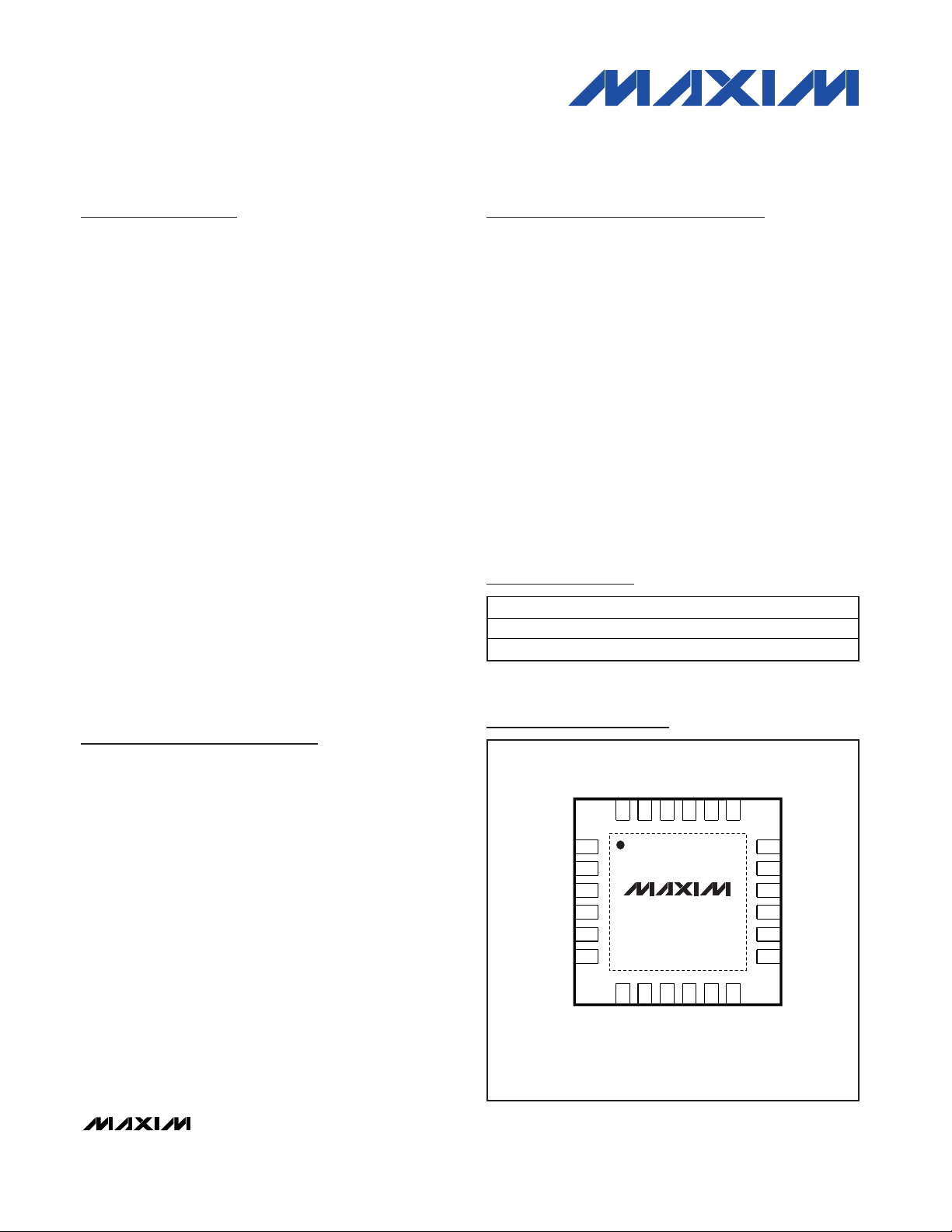
MAX3795
1Gbps to 4.25Gbps Multirate VCSEL
Driver with Diagnostic Monitors
________________________________________________________________ Maxim Integrated Products 1
Ordering Information
19-3387; Rev 0; 8/04
For pricing, delivery, and ordering information, please contact Maxim/Dallas Direct! at
1-888-629-4642, or visit Maxim’s website at www.maxim-ic.com.
PART
TEMP RANGE
PIN-PACKAGE
MAX3795ETG
24 Thi n QFN ( 4m m x 4m m )
MAX3795ETG+
24 Thi n QFN ( 4m m x 4m m )
24
23
22
21
20
19
PWRMON
REF
MD
COMP
VCCBIASMON
7
8
9
10
11
12
V
CC
TC1
TC2
GND
MODSET
PEAKSET
13
14
15
16
17
18
EXPOSED PAD IS CONNECTED TO GND
GND
OUT-
OUT+
V
CC
BIASSET
BIAS
6
5
4
3
2
1
SQUELCH
FAULT
IN-
IN+
TX_DISABLE
GND
MAX3795
THIN QFN (4mm x 4mm)
TOP VIEW
Pin Configuration
+Denotes lead-free package.
-40°C to +85°C
-40°C to +85°C
Page 2
MAX3795
1Gbps to 4.25Gbps Multirate VCSEL Driver
with Diagnostic Monitors
2 _______________________________________________________________________________________
ABSOLUTE MAXIMUM RATINGS
Stresses beyond those listed under “Absolute Maximum Ratings” may cause permanent damage to the device. These are stress ratings only, and functional
operation of the device at these or any other conditions beyond those indicated in the operational sections of the specifications is not implied. Exposure to
absolute maximum rating conditions for extended periods may affect device reliability.
Supply Voltage (VCC) ............................................-0.5V to +4.0V
Voltage at TX_DISABLE, IN+, IN-, FAULT,
SQUELCH, TC1, TC2, MODSET, PEAKSET, BIASSET,
BIAS, BIASMON, COMP, MD, REF,
PWRMON ...............................................-0.5V to (V
CC
+ 0.5V)
Voltage at OUT+, OUT-.........................(V
CC
- 2V) to (VCC+ 1V)
Current into FAULT ............................................ -1mA to +25mA
Current into OUT+, OUT- ....................................................60mA
Continuous Power Dissipation (T
A
= +85°C)
24-Pin Thin QFN
(derate 20.8mW/°C above +85°C).................................1354mW
Storage Temperature Range .............................-55°C to +150°C
Lead Temperature (soldering, 10s) .................................+300°C
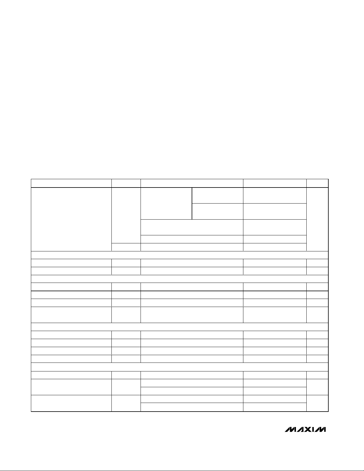
ELECTRICAL CHARACTERISTICS
(VCC= +2.97V to +3.63V, TA= -40°C to +85°C. Typical values are at VCC= +3.3V, TC1 and TC2 are shorted, PEAKSET open, TA=
+25°C, unless otherwise noted.)
PARAMETER
CONDITIONS
UNITS
I
MOD
= 2mA
P-P
35
SQUELCH set low,
TX_DISABLE set low,
peaking is not used
(Note 1)
I
MOD
= 15mA
P-P
71 81
Additional current when peaking is used,
R
PEAK
= 1.18kΩ
15
I
CC
Additional current when SQUELCH is high 5 10
Supply Current
Total current when TX_DISABLE is high 7
mA
FAULT OUTPUT
Output High Voltage V
OH
R
LOAD
= 10kΩ to 2.97V 2.4 V
Output Low Voltage V
OL
R
LOAD
= 4.7kΩ to 3.63V 0.4 V
TX_DISABLE INPUT
Input Impedance R
PULL
4.7 8
kΩ
Input High Voltage V
IH
2.0 V
Input Low Voltage V
IL
0.8 V
Power-Down Time
The time for I
CC
to reach I
CC-SHDN
when
TX_DISABLE transitions high
50 µs
SQUELCH
Squelch Threshold 25 85
mV
P-P
Squelch Hysteresis 6
mV
P-P
Time to Squelch Data (Note 3)
µs
Time to Resume from Squelch (Note 3)
µs
BIAS GENERATOR
Maximum Bias Pin Voltage
Referenced to V
CC
V
Minimum 1
Bias Current I
BIAS
Maximum 15
mA
5mA ≤ I
BIAS
≤ 15mA -8 +8
Accuracy of Programmed Bias
Current
∆BIAS
1mA ≤ I
BIAS
≤ 5mA -12
%
SYMBOL
MIN TYP MAX
I
CC-SHDN
V
BIAS-MAX
0.02 5.00
0.02 5.00
-0.65
10.0
+12
Page 3
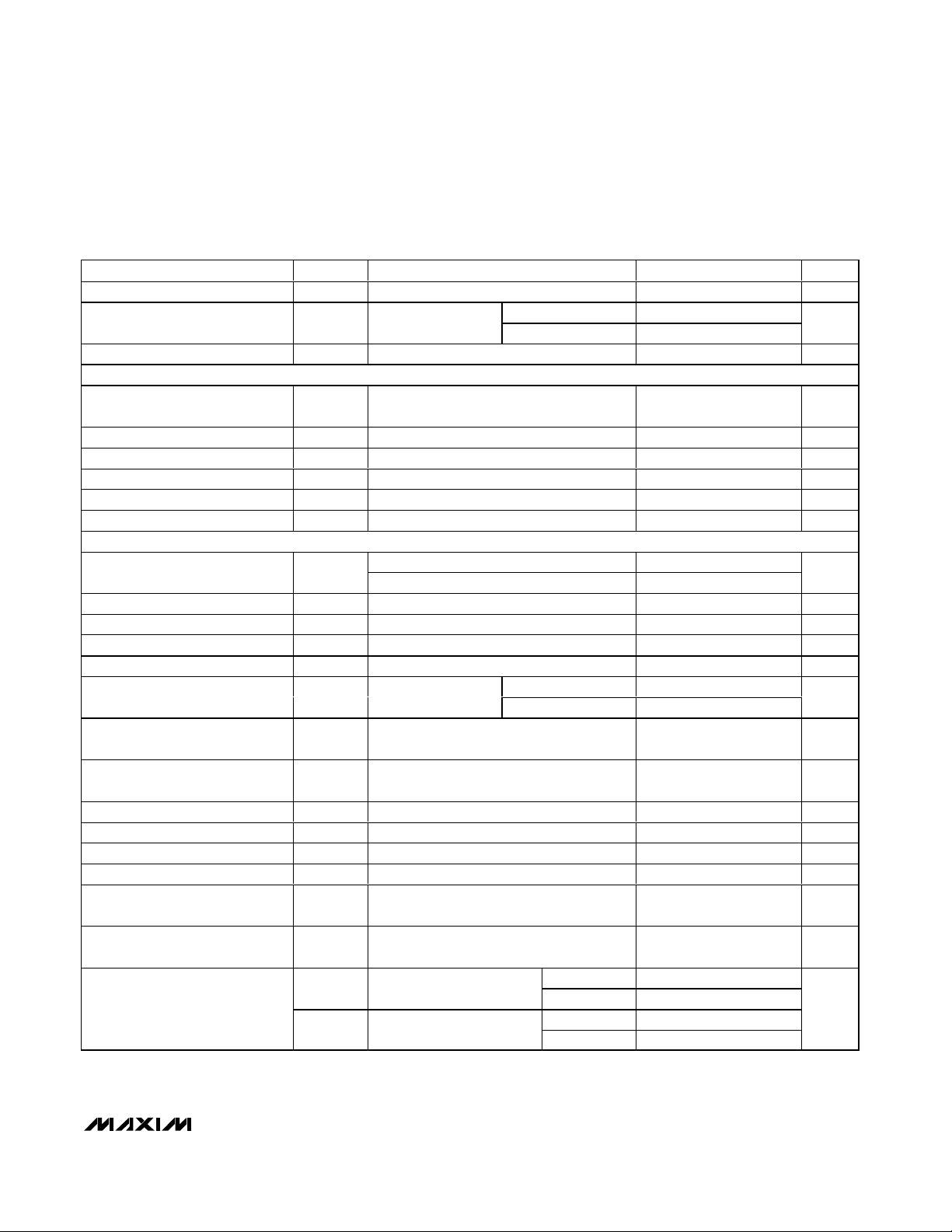
MAX3795
1Gbps to 4.25Gbps Multirate VCSEL Driver
with Diagnostic Monitors
_______________________________________________________________________________________ 3
ELECTRICAL CHARACTERISTICS (continued)
(VCC= +2.97V to +3.63V, TA= -40°C to +85°C. Typical values are at VCC= +3.3V, TC1 and TC2 are shorted, PEAKSET open, TA=
+25°C, unless otherwise noted.)
PARAMETER
SYMBOL
CONDITIONS
MIN
TYP
MAX
UNITS
Bias Current During Fault
Current out of the BIAS pin 1.5 10 µA
BIASMON Gain
I
BIASMON
/ I
BIAS
mA/mA
BIASMON Stability (Notes 2, 4) -10
%
AUTOMATIC POWER CONTROL (APC)
MD Nominal Voltage V
MD
APC loop is closed 1
0.2
2V
Voltage at REF V
REF
1.2 1.8 2.2 V
MD Voltage During Fault 0V
MD Input Current Normal operation (FAULT = low) -2 0.7 +2 µA
APC Time Constant C
COMP
= 0.047µF, ∆IPD / ∆I
LASER
= 0.02 90 µs
PWRMON Nominal Gain V
PWRMON
/ (V
REF
- VMD)
V/V
LASER MODULATOR (Load is 50Ω AC-Coupled to OUT+)
Minimum
Differential Input Voltage V
ID
Maximum 2.4
V
P-P
Input Common-Mode Voltage V
CM
V
Differential Input Resistance R
IN
85 100
Ω
Single-Ended Input Return Loss S11 f < 4GHz
dB
Differential Input Return Loss
f < 4GHz 11 dB
Minimum 2
Modulation Current I
MOD
Current into OUT+
R
LOAD
≤ 50Ω
Maximum 15
mA
Laser Modulation During Fault or
Squelch Active
DC tested 15 50
µA
P-P
Tolerance of Programmed
Modulation Current
TC1 is shorted to TC2 -10
%
Minimum Peaking Current R
PEAKSET
= 10kΩ 0.2 mA
Maximum Peaking Current R
PEAKSET
= 1kΩ 2mA
Peaking Current Duration 75 ps
Output Resistance
R
OUT
Single-ended resistance 42 50 58 Ω
Minimum Programmable
Temperature Coefficient
0
ppm/°C
Maximum Programmable
Temperature Coefficient
Temperature range 0°C to +70°C
ppm/°C
49 72
t
R
50Ω load, no peaking,
5mA ≤ I
MOD
≤ 15mA
+100°C 58
56 79
Modulation Transition Time
(Note 2)
t
F
50Ω load, no peaking,
5mA ≤ I
MOD
≤ 15mA
+100°C 64
ps
I
BIAS_OFF
G
BIASMON
SDD11
I
MOD_OFF
1mA < I
3mA ≤ I
< 3mA 0.0875 0.105 0.1375
BIAS
< 15mA 0.085 0.105 0.125
BIAS
V
REF
1.85 2.15 2.45
- 40°C to + 85° C
- 40°C to + 85° C
1.75
12.7
+5000
+10
-
0.25
115
+10
Page 4
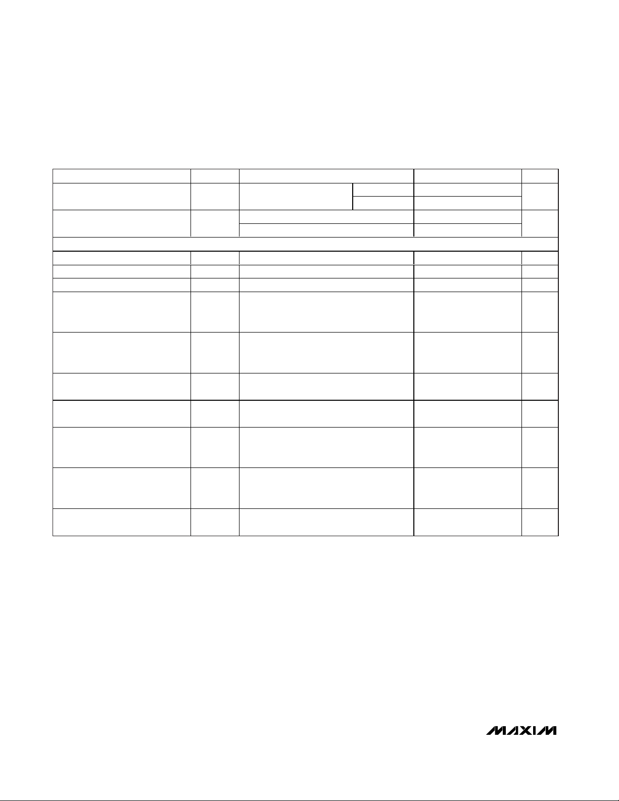
MAX3795
1Gbps to 4.25Gbps Multirate VCSEL Driver
with Diagnostic Monitors
4 _______________________________________________________________________________________
ELECTRICAL CHARACTERISTICS (continued)
(VCC= +2.97V to +3.63V, TA= -40°C to +85°C. Typical values are at VCC= +3.3V, TC1 and TC2 are shorted, PEAKSET open, TA=
+25°C, unless otherwise noted.)
PARAMETER
CONDITIONS
UNITS
8.4
Deterministic Jitter DJ
5m A ≤ I
M OD
≤ 15m A,
+100°C
ps
P-P
APC closed loop 0.5
Random Jitter RJ
APC open loop (Note 2) 0.5 0.9
ps
RMS
SAFETY FEATURES (see the Typical Operating Characteristics)
High-Current Fault Threshold V
BMTH
V
BIASMON
> V
BMTH
causes a fault 0.7 0.8 0.9 V
V
BIAS
Fault Threshold V
BTH
V
BIAS
referenced to V
CC
V
Power-Monitor Fault Threshold V
PMTH
V
PWRMON
> V
PMTH
causes a fault 0.7 0.8 0.9 V
TX Disable Time t_
OFF
Time from rising edge of TX_DISABLE to
I
BIAS
= I
BIAS_OFF
and I
MOD
= I
MOD_OFF
(Note 2)
1.8 5 µs
TX Disable Negate Time t_
ON
Time from rising edge of TX_DISABLE to
I
BIAS
and I
MOD
at 99% of steady state
(Note 2)
55 500 µs
Fault Reset Time t_
INIT
1
Time to set V
FAULT
= low after power-on or
after rising edge of TX_DISABLE (Note 2)
60 200 ms
Power-On Time t_
INIT
2
Time after power-on to transmitter-on with
TX_DISABLE low (Note 2)
60 200 ms
Fault Assert Time
Time from fault occurrence to V
FAULT
=
high; C
FAULT
< 20pF, R
FAULT
= 4.7kΩ
(Note 2)
1.4 50 µs
Fault Delay Time
Time from fault to I
BIAS
= I
BIAS_OFF
and
I
MOD
= I
MOD_OFF
; measured with a
continuously occurring fault (Note 2)
15µs
TX_DISABLE Reset
Time TX_DISABLE must be held high to
reset FAULT (Note 2)
1µs
Note 1: Supply current measurements exclude I
BIAS
from the total current.
Note 2: AC characteristics guaranteed by design and characterization.
Note 3: Measured by applying a pattern that contains 20µs of K28.5, followed by 5µs of zeros, then 20µs of K28.5, followed by 5µs
of ones. Data rate is equal to 2.5Gbps, with inputs filtered using 1.8GHz Bessel filters.
Note 4: Variation of bias monitor gain for any single part over the range of V
CC
, temperature, 3mA < I
BIAS
< 15mA.
Note 5: Deterministic jitter measured at 4.25Gbps with a K28.5 pattern (00111110101100000101).
SYMBOL
4.25G b p s, K28.5 ( N otes 2, 5)
- 40°C to + 85° C
MIN TYP MAX
15.6
12.7
-0.250 -0.2 -0.150
t_
FAULT
t_
FLTDLY
t_
RESET
Page 5
MAX3795
1Gbps to 4.25Gbps Multirate VCSEL Driver
with Diagnostic Monitors
_______________________________________________________________________________________ 5
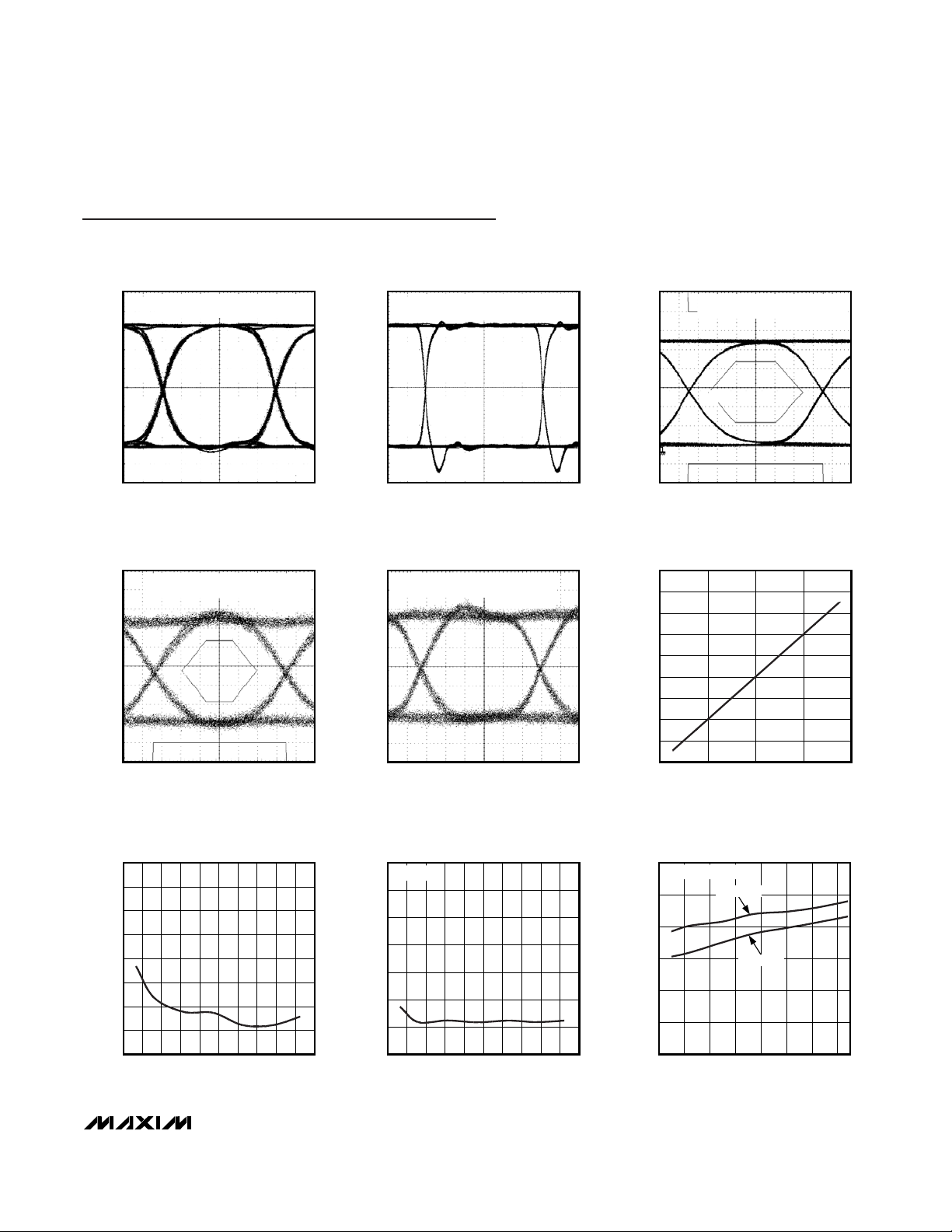
ELECTRICAL EYE DIAGRAM
MAX3795 toc01
40ps/div
75mV/div
4.25Gbps, K28.5, 10mA MODULATION,
PEAKING OFF
ELECTRICAL EYE DIAGRAM
MAX3795 toc02
152ps/div
75mV/div
1Gbps, K28.5, 10mA MODULATION,
R
PEAKSET
= 1.4kΩ
OPTICAL EYE DIAGRAM
MAX3795 toc03
135ps/div
1
2
3
1Gbps, K28.5, -3dBm, 850nm VCSEL
ADVANCED OPTICAL COMPONENTS,
HFE4191-541
OPTICAL EYE DIAGRAM
MAX3795 toc04
34ps/div
4.25Gbps, K28.5, -7dBm, 850nm VCSEL,
ADVANCED OPTICAL COMPONENTS
HFE4191-541
OPTICAL EYE DIAGRAM
MAX3795 toc05
50ps/div
3.125Gbps, K28.5, -7dBm, 850nm VCSEL,
ADVANCED OPTICAL COMPONENTS
HFE4191-541
I
BIASMON
vs. BIAS CURRENT
MAX3795 toc06
BIAS CURRENT (mA)
I
BIASMON
(mA)
1284
0.2
0.4
0.6
0.8
1.0
1.2
1.4
1.6
1.8
0
016
DETERMINISTIC JITTER
vs. MODULATION CURRENT
MAX3795 toc07
MODULATION CURRENT (mA
P-P
)
DETERMINISTIC JITTER (ps
P-P
)
5
10
15
20
25
30
35
40
0
024681012 14 16 18 20
RANDOM JITTER
vs. MODULATION CURRENT
MAX3795 toc08
MODULATION CURRENT (mA
P-P
)
RANDOM JITTER (ps
RMS
)
0.5
1.0
1.5
2.0
2.5
3.0
3.5
0
02468101214 16 18 20
I
BIAS
= 5mA
TRANSITION TIME
vs. MODULATION CURRENT
MAX3795 toc09
MODULATION CURRENT (mA)
TRANSITION TIME (ps)
10
20
30
40
50
60
70
024681012 14
MEASURED FROM 20%
FALL TIME
RISE TIME
Typical Operating Characteristics
(VCC= +3.3V, RTC= 0Ω, PEAKSET open, measured electrically with a 50Ω load AC-coupled to OUT+, TA= +25°C, unless otherwise
noted.)
Page 6

MAX3795
1Gbps to 4.25Gbps Multirate VCSEL Driver
with Diagnostic Monitors
6 _______________________________________________________________________________________
BIAS CURRENT vs. R
BIASSET
MAX3795 toc10
R
BIASSET
(Ω)
BIAS CURRENT (mA)
10
1
10
100
0.1
1 100
MODULATION CURRENT vs. R
MODSET
MAX3740A toc11
R
MODSET
(kΩ)
MODULATION CURRENT (mA
P-P
)
10
10
100
1
10010.1
MODULATION CURRENT TEMPCO
vs. R
TC
MAX3795 toc17
RTC (Ω)
TEMPCO (ppm/°C)
100k10k1k
500
1500
2500
3500
4500
5500
-500
100 1M
REFERENCED TO +25°C
MONITOR DIODE CURRENT
vs. R
PWRSET
MAX3795 toc12
R
PWRSET
(Ω)
MONITOR DIODE CURRENT (A)
1
10µ
100µ
1m
10m
1µ
010
SUPPLY CURRENT vs. TEMPERATURE
MAX3795 toc13
TEMPERATURE (°C)
SUPPLY CURRENT (mA)
603510-15
20
30
40
50
60
70
80
90
100
-40 85
I
MOD
= 2mA
I
MOD
= 15mA
INPUT RETURN LOSS
MAX3795 toc14
FREQUENCY (Hz)
S
11
(dB)
1G
-30
-25
-20
-15
-10
-5
0
-35
100 10G
DIFFERENTIAL
MEASUREMENT
AT IN±
OUTPUT RETURN LOSS
MAX3795 toc15
FREQUENCY (Hz)
S
22
(dB)
1G
-40
-35
-30
-25
-20
-15
-10
-5
0
-45
100 10G
SINGLE-ENDED
MEASUREMENT
MODULATION CURRENT
vs. TEMPERATURE
MAX3795 toc16
TEMPERATURE (°C)
MODULATION CURRENT (mA
P-P
)
8070605040302010
5
6
7
8
9
10
11
4
090
R
MODSET
= 1.8kΩ
RTC = 1kΩ
RTC = 500kΩ
RTC = 100kΩ
RTC = 60kΩ
RTC = 10kΩ
RTC = 5kΩ
RTC = 100Ω
Typical Operating Characteristics (continued)
(VCC= +3.3V, RTC= 0Ω, PEAKSET open, measured electrically with a 50Ω load AC-coupled to OUT+, TA= +25°C, unless otherwise
noted.)
Page 7

MONITOR DIODE CURRENT
vs. TEMPERATURE
MAX3795 toc18
TEMPERATURE (°C)
MONITOR DIODE CURRENT (µA)
6035-15 10
125
150
175
200
225
250
275
300
100
-40 85
MAX3795
1Gbps to 4.25Gbps Multirate VCSEL Driver
with Diagnostic Monitors
_______________________________________________________________________________________ 7
HOT PLUG WITH TX_DISABLE LOW
MAX3795 toc19
20ms/div
TX_DISABLE
V
CC
LASER
OUTPUT
FAULT
LOW
t_INIT = 60ms
3.3V
0V
LOW
STARTUP WITH SLOW RAMPING SUPPLY
MAX3795 toc20
20ms/div
TX_DISABLE
V
CC
LASER
OUTPUT
FAULT
LOW
t_INIT = 62ms
3.3V
LOW
0V
FAULT RECOVERY TIME
MAX3795 toc24
40µs/div
TX_DISABLE
V
PWRMON
LASER
OUTPUT
FAULT
LOW
t_INIT = 54µs
HIGH
EXTERNAL
FAULT
REMOVED
LOW
LOW
HIGH
FREQUENT ASSERTION OF TX_DISABLE
MAX3795 toc25
200µs/div
TX_DISABLE
V
PWRMON
LASER
OUTPUT
FAULT
EXTERNALLY
FORCED FAULT
Typical Operating Characteristics (continued)
(VCC= +3.3V, RTC= 0Ω, PEAKSET open, measured electrically with a 50Ω load AC-coupled to OUT+, TA= +25°C, unless otherwise
noted.)
TX_DISABLE NEGATE TIME
MAX3795 toc21
40µs/div
TX_DISABLE
V
CC
LASER
OUTPUT
FAULT
t_ON = 131µs
3.3V
LOW
LOW
HIGH
TRANSMITTER DISABLE
MAX3795 toc22
1µs/div
TX_DISABLE
V
CC
LASER
OUTPUT
FAULT
LOW
t_OFF = 2.2µs
3.3V
HIGH
LOW
RESPONSE TO FAULT
MAX3795 toc23
4µs/div
TX_DISABLE
V
PWRMON
LASER
OUTPUT
FAULT
LOW
t_FAULT = 2.16µs
HIGH
EXTERNALLY
FORCED
FAULT
LOW
Page 8

MAX3795
1Gbps to 4.25Gbps Multirate VCSEL Driver
with Diagnostic Monitors
8 _______________________________________________________________________________________
Pin Description
PIN NAME FUNCTION
1, 10, 13 GND Ground
2
Transmit Disable. Driver output is disabled when TX_DISABLE is high or left unconnected. The
driver output is enabled when the pin is asserted low.
3 IN+ Noninverted Data Input
4 IN- Inverted Data Input
5 FAULT
Fault Indicator. Open-drain output with ESD protection. FAULT is asserted high during a
fault condition.
6
Squelch Enable. Squelch is enabled when the pin is set high. Squelch is disabled when the pin is
set low or left open.
7, 16, 20 V
CC
+3.3V Supply Voltage
8 TC1
Temperature Compensation Set Pin 1. A resistor placed between TC1 and TC2 (R
TC
) programs the
temperature coefficient of the laser modulation current.
9 TC2
Temperature Compensation Set Pin 2. A resistor placed between TC1 and TC2 (R
TC
) programs the
temperature coefficient of the laser modulation current.
11 MODSET
Modulation Set. A resistor connected from MODSET to ground (R
MODSET
) programs the desired
modulation current amplitude.
12 PEAKSET
Peaking Current Set. A resistor connected between PEAKSET and ground (R
PEAKSET
) programs the
peaking current amplitude. To disable peaking, leave PEAKSET open.
14 OUT- Inverted Modulation Current Output
15 OUT+ Noninverted Modulation Current Output
17 BIASSET
Bias-Current Set. When a closed-loop configuration is used, connect a 1.7kΩ resistor between
ground and BIASSET to program the maximum bias current. When an open configuration is used,
connect a resistor between BIASSET and ground (R
BIASSET
) to program the VCSEL bias current.
18 BIAS Bias-Current Output
19 BIASMON
Bias-Current Monitor. The output of BIASMON is a sourced current proportional to the bias current.
A resistor connected between BIASMON and ground (R
BIASMON
) can be used to form a ground-
referenced bias monitor.
21 COMP
Compensation Pin. A capacitor between COMP and MD compensates the APC. A typical value of
0.047µF is recommended. For open-loop configuration, short the COMP pin to GND to deactivate
the APC circuit.
22 MD Monitor Diode Connection
23 REF
Refer ence P i n. Refer ence m oni tor used for AP C . A r esi stor b etw een RE F and M D ( R
P WRS E T
) p r og r am s
the p hotom oni tor cur r ent w hen the AP C l oop i s cl osed .
24 PWRMON
Average Power Monitor. The pin is used to monitor the transmit optical power. For open-loop
configuration, connect PWRMON to GND.
EP
Ground. Must be soldered to the circuit board ground for proper thermal and electrical
performance. See the Layout Considerations section.
TX_DISABLE
SQUELCH
Exposed Pad
Page 9

Detailed Description
The MAX3795 contains a bias generator with APC,
safety circuit, and a laser modulator with optional peaking compensation (see the Functional Diagram).
Bias Generator
Figure 1 shows the bias-generator circuitry that contains
a power-control amplifier and smooth-start circuitry. An
internal pnp transistor provides DC laser current to bias
the laser in a light-emitting state. The APC circuitry
adjusts the laser-bias current to maintain average power
over temperature and changing laser properties. The
smooth-start circuitry prevents current spikes to the laser
during power-up or enable, ensuring compliance with
safety requirements and extending the life of the laser.
The MD input is connected to the cathode of a monitor
diode, which is used to sense laser power. The BIAS
output is connected to the anode of the laser through an
inductor or ferrite bead. The power-control amplifier drives a current amplifier to control the laser’s bias current.
During a fault condition, the bias current is disabled.
The PWRMON output provides a voltage proportional to
average laser power given by:
V
PWRMON
= 2 x IPDx R
PWRSET
where V
PWRMON
= 0.4V (typ)
The BIASMON output provides a current proportional to
the laser bias current given by:
I
BIASMON
= I
BIAS
x G
BIASMON
When APC is not used (no monitor diode), connect the
COMP and PWRMON pins to GND. In this mode, bias
current is set by the resistor (R
BIASSET
) between the
BIASSET pin and GND. When a closed-loop configuration is used, connect a 1.7kΩ resistor between ground
and BIASSET to set the maximum bias current.
Safety Circuit
The safety circuit contains an input disable
(TX_DISABLE), a latched fault output (FAULT), and fault
detectors (Figure 2). This circuit monitors the operation
of the laser driver and forces a shutdown (disables
laser) if a fault is detected (Table 1). Table 2 contains
the circuit’s response to various single-point failures.
The transmit fault condition is latched until reset by a
toggle of TX_DISABLE or VCC. The FAULT pin should
be pulled high with a 4.7kΩ to 10kΩ resistor.
MAX3795
1Gbps to 4.25Gbps Multirate VCSEL Driver
with Diagnostic Monitors
_______________________________________________________________________________________ 9
C
COMP
COMP BIASSET
R
PWRSET
MD
1.8V
(2VBE + 0.2)
REF
CURRENT
AMPLIFIER
POWER-
CONTROL
AMPLIFIER
ENABLE
200Ω
R
BIASSET
PWRMON
BIAS GENERATOR
SMOOTH-
START
R
BIASMON
BIASMON
FERRITE
BEAD
BIAS
1.6V
(2V
BE
)
2X
I
BIAS
34
I
PD
I
BIAS
9
MAX3795
1V
Figure 1. Bias Generator
PIN FAULT CONDITION
BIAS V
BIAS
> VCC - 0.2V
BIASMON V
BIASMON
> 0.8V
PWRMON V
PWRMON
> 0.8V
Table 1. Fault Conditions
Page 10

MAX3795
1Gbps to 4.25Gbps Multirate VCSEL Driver
with Diagnostic Monitors
10 ______________________________________________________________________________________
Modulation Circuit
The modulation circuitry consists of an input buffer, a
current mirror, and a high-speed current switch (Figure
3). The modulator drives up to 15mA of modulation into
a 50Ω VCSEL load.
The amplitude of the modulation current is set with
resistors at MODSET and temperature coefficient (TC1,
TC2) pins. The resistor at MODSET (R
MODSET
) programs the temperature-stable portion of the modulation
current, and the resistor between TC1 and TC2 (RTC)
programs the temperature coefficient of the modulation
PIN NAME
CIRCUIT RESPONSE TO
V
CC
SHORT
CIRCUIT RESPONSE TO
GND SHORT
CIRCUIT RESPONSE TO
OPEN
FAULT Does not affect laser power. Does not affect laser power. Does not affect laser power.
Modulation and bias current are
disabled.
Normal condition for circuit
operation.
Modulation and bias current are
disabled.
IN+ Does not affect laser power.
Does not affect laser power.
Does not affect laser power.
IN- Does not affect laser power.
Does not affect laser power.
Does not affect laser power.
Does not affect laser power.
Does not affect laser power.
Does not affect laser power.
TC1 Does not affect laser power. Does not affect laser power.
The laser modulation is decreased,
but average power is not affected.
TC2
The laser modulation is increased,
but average power is not affected.
Modulation current is disabled.
The laser modulation is decreased,
but average power is not affected.
MODSET Modulation current is disabled.
The laser modulation is increased,
but average power is not affected.
The laser modulation is decreased,
but average power is not affected.
PEAKSET Does not affect laser power.
Does not affect laser power.
Does not affect laser power.
OUT+ Modulation current is disabled.
Modulation current is disabled.
Modulation current is disabled.
OUT- Does not affect laser power.
Does not affect laser power.
Does not affect laser power.
BIASSET Laser bias is disabled.
Fault state* occurs.
Laser bias is disabled.
BIAS
Fault state* occurs. Note that VCSEL
emissions may continue. Care must
be taken to prevent this condition.
This disables the VCSEL. This disables the VCSEL.
Fault state* occurs.
Does not affect laser power.
Fault state* occurs.
COMP
The bias current is reduced, and the
average power of the laser output is
reduced.
I
BIAS
increases to the value
determined by R
BIASSET
. If the biasmonitor fault threshold is exceeded,
a fault is signaled.
APC loop will be unstable.
If the bias-monitor fault threshold is
exceeded, a fault is signaled.
MD
I
BIAS
increases to the value
determined by R
BIASSET
. If the biasmonitor fault threshold is exceeded,
a fault is signaled.
The bias current is reduced, and the
average power of the laser output is
reduced.
I
BIAS
increases to the value
determined by R
BIASSET
. If the bias
monitor fault threshold is exceeded,
a fault is signaled.
REF
I
BIAS
increases to the value
determined by R
BIASSET
. If the biasmonitor fault threshold is exceeded,
a fault is signaled.
The bias current is reduced, and the
average power of the laser output is
reduced.
The bias current is reduced, and the
average power of the laser output is
reduced.
PWRMON Fault state* occurs. Does not affect laser power. Does not affect laser power.
*A fault state asserts the FAULT pin, disables the modulator output, and disables the bias output.
Table 2. Circuit Response to Various Single-Point Faults (Closed-Loop APC Configuration)
TX_DISABLE
SQUELCH
BIASMON
Page 11

MAX3795
1Gbps to 4.25Gbps Multirate VCSEL Driver
with Diagnostic Monitors
______________________________________________________________________________________ 11
S
R
Q
R-S LATCH
HIGH-POWER FAULT
HIGH-CURRENT FAULT
V
BIAS
FAULT
BIAS
BIASMON
PWRMON
POR
TX_DISABLE
TX_DISABLE
0.8V
0.8V
V
CC
- 0.2V
FAULT
ENABLE
SAFETY CIRCUIT
FAULT
OUTPUT
MAX3795
Figure 2. Safety Circuit
V
CC
R
OUT
100Ω
CURRENT AMPLIFIER 40x
ENABLE
IN+
IN-
OUT+
OUT-
TC1
MODSET
R
TC
R
MODSET
MODULATION
CURRENT GENERATOR
INPUT BUFFER
CURRENT SWITCH
TEMPERATURE
COMPENSATION
TC2
SIGNAL
DETECT
SQUELCH
PEAKING
CONTROL
PEAKSET
200Ω
R
OUT
1V
R
PEAKSET
MAX3795
Figure 3. Modulation Circuit
Page 12

current. For appropriate RTCand R
MODSET
values, see
the Typical Operating Characteristics.
Design Procedure
Select Laser
Select a communications-grade laser with a rise time of
90ps or better for 4.25Gbps applications. Use a highefficiency laser that requires low modulation current and
generates a low-voltage swing. Trim the leads to reduce
laser package inductance. The typical package leads
have inductance of 25nH per inch (1nH/mm). This
inductance causes a large voltage swing across the
laser. A compensation filter network can also be used to
reduce ringing, edge speed, and voltage swing.
Programming Modulation Current
A resistor (R
MODSET
) placed between the MODSET pin
and ground controls the modulation current out of the
MAX3795 to the VCSEL. The modulation current is
given by the following:
It is important to note that the load impedance of the
VCSEL affects the modulation current being sourced by
the MAX3795. The Modulation Current vs. R
MODSET
graph in the Typical Operating Characteristics shows the
current into a 50Ω load. Capacitance at the MODSET pin
should be ≤20pF.
Programming Bias Current
The bias current output of the MAX3795 is controlled by
a resistor (R
BIASSET
) placed between the BIASSET pin
and ground. In open-loop operation, BIASSET controls
the bias current level of the VCSEL. In closed-loop
operation (APC); the R
BIASSET
controls the maximum
allowed bias current. The open-loop bias current is
given by the following:
The Bias Current vs. R
BIASSET
graph in the Typical
Operating Characteristics shows the current into a 50Ω
load. Capacitance at the BIASSET pin should be
≤20pF.
Programming Modulation-Current Tempco
Compute the required modulation tempco from the
slope efficiency of the laser at TA= +25°C and at a
higher temperature. Then select the value of RTCfrom
the Typical Operating Characteristics. For example,
suppose a laser has a slope efficiency (SE) of
0.021mW/mA at +25°C, which reduces to 0.018mW/mA
at +85°C. The temperature coefficient is given by the
following:
From the Typical Operating Characteristics, the value
of RTC, which offsets the tempco of the laser, is 9kΩ. If
modulation temperature compensation is not desired,
short TC1 and TC2.
Programming the APC Loop
Program the average optical power by adjusting
R
PWRSET
. To select the resistance, determine the
desired monitor current to be maintained over temperature and lifetime. See the Monitor Diode Current vs.
R
PWRSET
graph in the Typical Operating Characteristics,
and select the value of R
PWRSET
that corresponds to the
required current.
Laser tempco
SE SE
SE
ppm C
=
−
×−
×
=°
−
()
()
/
85 25
25
6
85 25
10
2380
I
R
BIAS
BIASSET
=
+
×
12
200
34
.
I
R
R
RR
MOD
MODSET
OUT
OUT LOAD
=
+
×
×
+
1
200
40
MAX3795
1Gbps to 4.25Gbps Multirate VCSEL Driver
with Diagnostic Monitors
12 ______________________________________________________________________________________
MAX3795
IN+
IN-
1nH
1nH
0.5pF
0.5pF
15pF
V
CC
50Ω
50Ω
1kΩ
V
CC
V
CC
PACKAGE
Figure 4. Simplified Input Structure
Page 13

MAX3795
1Gbps to 4.25Gbps Multirate VCSEL Driver
with Diagnostic Monitors
______________________________________________________________________________________ 13
The low frequency cutoff of a transmitter using APC is
given by:
Input Termination Requirements
The MAX3795 data inputs are SFP MSA compatible. Onchip, 100Ω differential input impedance is provided for
optimal termination (Figure 4). Because of the on-chip
biasing network, the MAX3795 inputs self-bias to the
proper operating point to accommodate AC-coupling.
Applications Information
Interface Models
Figures 4 and 5 show simplified input and output circuits
for the MAX3795 laser driver. Figure 6 shows the fault circuit interface.
Layout Considerations
To minimize inductance, keep the connections between
the MAX3795 output pins and laser diode as short as
possible. Use multilayer boards with uninterrupted
ground planes to minimize EMI and crosstalk.
Exposed-Pad (EP) Package
The exposed pad on the 24-pin thin QFN provides a very
low thermal resistance path for heat removal from the IC.
The pad is also electrical ground on the MAX3795 and
must be soldered to the circuit board ground for proper
thermal and electrical performance. Refer to Maxim
Application Note HFAN-08.1: Thermal Considerations for
QFN and Other Exposed-Pad Packages for additional
information.
Laser Safety and IEC 825
The International Electrotechnical Commission (IEC)
determines standards for hazardous light emissions from
fiber-optic transmitters. IEC 825 defines the maximum
light output for various hazard levels. The MAX3795 provides features that facilitate compliance with IEC 825. A
common safety precaution is single-point fault tolerance,
whereby one unplanned short, open, or resistive connection does not cause excess light output. Using this laser
driver alone does not ensure that a transmitter design is
compliant with IEC 825. The entire transmitter circuit and
component selections must be considered. Customers
must determine the level of fault tolerance required by
their applications, recognizing that Maxim products are
not designed or authorized for use as components in
systems intended for surgical implant into the body, for
applications intended to support or sustain life, or for any
other application where the failure of a Maxim product
could create a situation where personal injury or death
may occur.
I
VV
R
V
R
PD
REF MD
PWRSET PWRSET
=
−
≈
02.
Figure 6. Fault Circuit Interface
MAX3795
V
CC
FAULT
Figure 5. Simplified Output Structure
f
I
IC
dB
PD
LASER APC
3
1
250
≈×
×× ×
∆
∆π
V
CC
50W
50W
PACKAGE
0.5pF
0.5pF
MAX3795
1nH
1nH
OUT-
OUT+
Page 14

PART PACKAGE TYPE
PACKAGE CODE
MAX3795ETG
24 Thin QFN
T2444-1
MAX3795ETG+
24 Thin QFN
T2444-1
Chip Information
TRANSISTOR COUNT: 3806
PROCESS: SiGe BIPOLAR
Package Information
For the latest package outline information, go to
www.maxim-ic.com/packages
.
MAX3795
1Gbps to 4.25Gbps Multirate VCSEL Driver
with Diagnostic Monitors
14 ______________________________________________________________________________________
Functional Diagram
SAFETY
CIRCUITRY
TX_DISABLE
FAULT
V
CC
IN+
IN-
OUTOUT+
MODULATION CURRENT
GENERATOR
BIAS
GENERATOR
WITH APC
ENABLE
ENABLE
100Ω
LASER
MODULATOR
PEAKING
CONTROL
COMP MD REF PWRMON
BIAS
BIASSET
BIASMON
PEAKSET
TC1 TC2 MODSET
SQUELCH
SIGNAL
DETECT
MAX3795
R
OUT
R
OUT
(4mm x 4mm x 0.8mm)
(4mm x 4mm x 0.8mm)
Page 15

MAX3795
1Gbps to 4.25Gbps Multirate VCSEL Driver
with Diagnostic Monitors
Maxim cannot assume responsibility for use of any circuitry other than circuitry entirely embodied in a Maxim product. No circuit patent licenses are
implied. Maxim reserves the right to change the circuitry and specifications without notice at any time.
Maxim Integrated Products, 120 San Gabriel Drive, Sunnyvale, CA 94086 408-737-7600 ____________________ 15
© 2004 Maxim Integrated Products Printed USA is a registered trademark of Maxim Integrated Products.
Typical Application Circuit
V
CC
REF
COMP
MD
BIAS
OUT+
OUT-
MODSET
BIASSET
R
BIASSET
PWRMON
TC1
TC2
IN+
IN-
TX_DISABLE
FAULT
SQUELCH
GND
0.047µF
+3.3V
0.1µF
0.1µF
R
TC
†
†
OPTIONAL COMPONENT
*FERRITE BEAD
PEAKSET
R
PEAKSET
†
0.01µF
0.01µF
50Ω
L1*
C
F
†
R
F
†
0.01µF
0.01µF
56Ω
L1*
L2*
C
F
†
R
F
†
BIASMON
R
BIASMON
4.7kΩ
†
R
PWRSET
R
MODSET
MAX3795
SINGLE-ENDED DRIVE
DIFFERENTIAL DRIVE
 Loading...