

Page 1
General Description
The MAX3744/MAX3745 transimpedance amplifiers provide a compact, low-power solution for communication
up to 2.7Gbps. They feature 330nA input-referred noise
at 2.1GHz bandwidth (BW) with 0.85pF input capacitance. The parts also have >2mA
P-P
AC input overload.
Both parts operate from a single +3.3V supply and consume 93mW. The MAX3744/MAX3745 are in a compact
30-mil x 50-mil die and require no external compensation capacitor. A space-saving filter connection is provided for positive bias to the photodiode through an
on-chip 580Ω resistor to VCC. These features allow
easy assembly into a low-cost TO-46 or TO-56 header
with a photodiode.
The MAX3744 and MAX3748A receiver chip set provides an RSSI output using a Maxim-proprietary* interface technique. The MAX3744 preamplifier, MAX3748A
postamplifier, and DS1858/DS1859 SFP controller meet
all the SFF-8472 digital diagnostic requirements.
Applications
Up to 2.7Gbps SFF/SFP Optical Receivers
Optimized for Small-Form-Factor Pluggable (SFP)
Optical Receivers
Features
♦ Up to 2.7Gbps (NRZ) Data Rates
♦ RSSI Implementation in 4-Pin TO46 Header
(MAX3744)
♦ 10ps
P-P
Deterministic Jitter for <100µA
P-P
Input
Current
♦ 330nA
RMS
Input-Referred Noise at 2.1GHz
Bandwidth
♦ 28mA Supply Current at +3.3V
♦ 2GHz Small-Signal Bandwidth
♦ 2.0mA
P-P
AC Overload
♦ Die Size: 30 mils x 50 mils
MAX3744/MAX3745
2.7Gbps SFP Transimpedance
Amplifiers with RSSI
________________________________________________________________ Maxim Integrated Products 1
Ordering Information
V
CC
FILTER
4-PIN TO CAN
400pF
400pF
IN
OUT+
OUT-
GND
OUT+
0.1
µ
F
0.1
µ
F
3.3k
Ω
IN+
V
CC
IN-
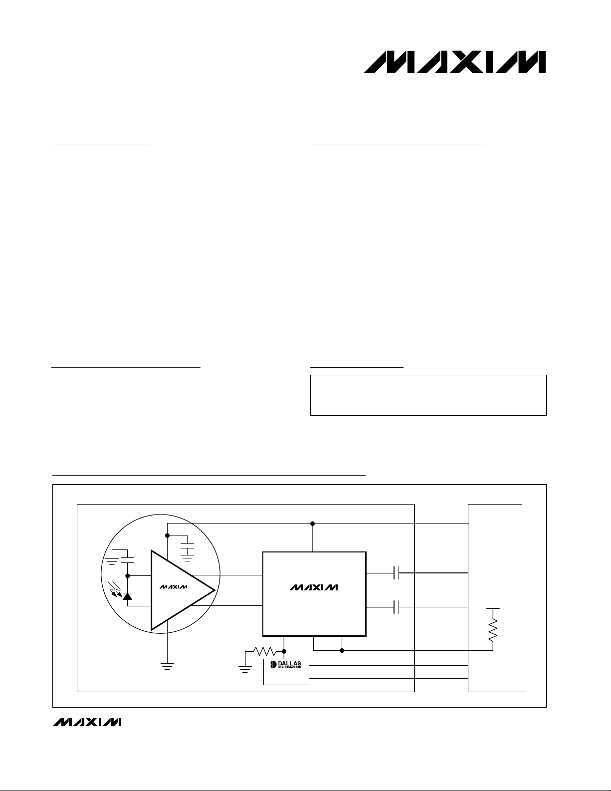
RSSI
DISABLE LOS
OUT-
MAX3748A
SFP OPTICAL RECEIVER
HOST
BOARD
MOD-DEF1
MOD-DEF2
4.7kΩ
TO
10kΩ
V
CC
MAX3744
DS1858/
DS1859
3.3V
Typical Application Circuit
19-2927; Rev 0; 7/03
For pricing, delivery, and ordering information, please contact Maxim/Dallas Direct! at
1-888-629-4642, or visit Maxim’s website at www.maxim-ic.com.
**Dice are guaranteed to operate from -40°C to +85°C, but are
tested only at T
A
= +25°C.
*Patent pending
MAX3744E/D -40°C to +85°C Dice**
MAX3745E/D -40°C to +85°C Dice**
PART TEMP RANGE PIN-PACKAGE
Page 2
MAX3744/MAX3745
2.7Gbps SFP Transimpedance
Amplifiers with RSSI
2 _______________________________________________________________________________________
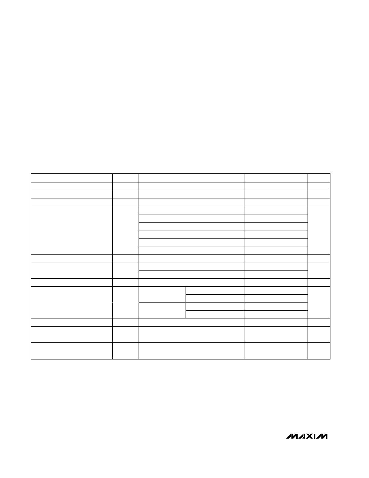
ABSOLUTE MAXIMUM RATINGS
ELECTRICAL CHARACTERISTICS
(VCC= +2.97V to +3.63V and TA= -40°C to +85°C. Typical values are at VCC= +3.3V, source capacitance (CIN) = 0.85pF, and TA=
+25°C, unless otherwise noted.) (Notes 1, 2)
Stresses beyond those listed under “Absolute Maximum Ratings” may cause permanent damage to the device. These are stress ratings only, and functional
operation of the device at these or any other conditions beyond those indicated in the operational sections of the specifications is not implied. Exposure to
absolute maximum rating conditions for extended periods may affect device reliability.
Power-Supply Voltage (VCC) .................................-0.5V to +6.0V
Continuous CML Output Current
(OUT+, OUT-) ............................................. -25mA to +25mA
Continuous Input Current (IN)...............................-4mA to +4mA
Continuous Input Current (FILTER).......................-8mA to +8mA
Operating Junction Temperature Range (T
J
) ....-55°C to +150°C
Storage Ambient Temperature Range (T
STG
) ...-55°C to +150°C
Die Attach Temperature...................................................+400°C
Supply Current I
Input Bias Voltage 1.0 V
Input Overload (Note 3) 2 mA
Input-Referred Noise I
Differential Transimpedance Differential output, IIN = 40µA
Small-Signal Bandwidth (Note 3) BW
Low-Frequency Cutoff -3dB, input current = 20µA
Deterministic Jitter
(Notes 3, 5)
Filter Resistance 510 580 690 Ω
Differential Output Resistance
(OUT+, OUT-)
Maximum Differential Output
Voltage
PARAMETER SYMBOL CONDITIONS MIN TYP MAX UNITS
Including CML output current (IIN = 0) 28 41 mA
CC
CIN = 0.85pF, BW = 933MHz 206
CIN = 0.85pF, BW = 2.1GHz 330 430
CIN = 0.85pF, BW = 18GHz 620
N
CIN = 0.6pF, BW = 933MHz 206
CIN = 0.6pF, BW = 2.1GHz 300 380
CIN = 0.6pF, BW = 18GHz 550
-3dB, CIN = 0.6pF 1.8 2
= 0.85pF 1.6 1.8
IN
< input ≤
P-P
P-P 2.7Gbps, 2
< input ≤
P-P
P-P
(output in limited state)
CC
V
DJ
OD
-3dB, C
100µA
2mA
10µA
100µA
Input > 50µA
V
AVE
(Note 3) 30 kHz
AVE
2.1Gbps, K28.5 pattern 14 31
31
-1 pattern 24
2.1Gbps, K28.5 pattern 10 16
2.7Gbps, 231-1 pattern 20
, output termination 50Ω to
AVE
2.8 3.5 4.5 kΩ
85 100 115 Ω
220 280 400 mV
nA
ps
P-P
RMS
GHz
P-P
P-P
Page 3
MAX3744/MAX3745
2.7Gbps SFP Transimpedance
Amplifiers with RSSI
_______________________________________________________________________________________ 3
ELECTRICAL CHARACTERISTICS (continued)
(VCC= +2.97V to +3.63V and TA= -40°C to +85°C. Typical values are at VCC= +3.3V, source capacitance (CIN) = 0.85pF, and TA=
+25°C, unless otherwise noted.) (Notes 1, 2)
Note 1: Die parameters are production tested at room temperature only, but are guaranteed by design and characterization from
-40°C to +85°C.
Note 2: Source capacitance represents the total capacitance at the IN pad during characterization of the noise and bandwidth para-
meters.
Note 3: Guaranteed by design and characterization.
Note 4: Input-referred noise is:
Note 5: Deterministic jitter is the sum of pulse-width distortion (PWD) and pattern-dependent jitter (PDJ).
Note 6: Power-supply noise rejection PSNR = -20log(∆V
OUT
/ ∆VCC), where ∆V
OUT
is the differential output voltage and ∆VCCis the
noise on V
CC
.
Note 7:
A
IIAIIA
A
where I
II
RSSI range is from I A to A
RSSI
OUT CM IN OUT CM IN
OUT CM
OUT OUT
IN
=
=− =
=
+
=
+−
__
_
()()
400 0
400
2
6 500
µµ
µ
µµ
RMS output noise
Gain at f MHz=
100
Single-Ended Output CommonMode Minimum Level (MAX3744)
Output Data Transition Time
Differential Output Return Loss
Power-Supply Noise Rejection PSNR
RSSI Gain (MAX3744) A
RSSI Gain Stability (MAX3744)
PARAMETER SYMBOL CONDITIONS MIN TYP MAX UNITS
RSSI
Relative to V
Input > 200µA
(Note 3)
Frequency ≤ 1GHz 17
1GHz < frequency ≤ 2GHz 10
I
= 0
IN
(Note 6)
(Note 7) 21 A/A
10log(A
A
at 3.3V, +25°C (Note 3)
RSSI
, IIN = 1mA
CC
20% to 80% rise/fall time
P-P
RSSI/ARSSI-NOM
AVE
f < 1MHz 46
1MHz ≤ f < 10MHz 34
) where A
RSSI-NOM
540 490 mV
=
80 140 ps
0.24 dB
TBD
dB
Page 4

MAX3744/MAX3745
2.7Gbps SFP Transimpedance
Amplifiers with RSSI
4 _______________________________________________________________________________________
Typical Operating Characteristics
(V
CC
= +3.3V, CIN= 0.85pF, TA = +25°C, unless otherwise noted.)
60ps/div
EYE DIAGRAM
INPUT = 2mA
P-P
, DATA RATE = 2.7Gbps
30mV/div
MAX3744 toc09
223-1 PATTERN
60ps/div
EYE DIAGRAM
INPUT = 2mA
P-P
, DATA RATE = 2.1Gbps
30mV/div
MAX3744 toc08
K28-5 PATTERN
60ps/div
EYE DIAGRAM
INPUT = 20µA
P-P
, DATA RATE = 2.1Gbps
5mV/div
MAX3744 toc06
K28-5 PATTERN
50
10M 10G1G100M
FREQUENCY RESPONSE
75
60
55
70
65
MAX3744 toc03
FREQUENCY (Hz)
GAIN (dB)
60ps/div
EYE DIAGRAM
INPUT = 20µA
P-P
, DATA RATE = 2.7Gbps
6mV/div
MAX3744 toc07
223-1 PATTERN
200
400
300
600
500
700
800
-40 20 40-20 0 60 80 100
INPUT-REFERRED NOISE
vs. TEMPERATURE
MAX3744 toc01
TEMPERATURE (°C)
INPUT-REFERRED NOISE (nA
RMS
)
UNFILTER
CIN = 1.5pF
CIN = 0.85pF
CIN = 0.5pF
200
400
300
600
500
700
800
-40 20 40-20 0 60 80 100
INPUT-REFERRED NOISE
vs. TEMPERATURE
MAX3744 toc02
TEMPERATURE (°C)
INPUT-REFERRED NOISE (nA
RMS
)
BW = 2.1GHz
CIN = 1.5pF
CIN = 0.85pF
CIN = 0.5pF
DETERMINISTIC JITTER
vs. INPUT AMPLITUDE
MAX3744 toc04
INPUT AMPLITUDE (mA
P-P
)
DETERMINISTIC JITTER (ps
P-P
)
10.1
10
20
30
40
50
0
0.01 10
2.7Gbp SONET
2.1Gbps FIBRE CHANNEL
60
65
70
75
-40 0 20-20 40 60 80 100
SMALL-SIGNAL TRANSIMPEDANCE
vs. TEMPERATURE
MAX3744 toc05
TEMPERATURE (°C)
TRANSIMPEDANCE (dB Ω)
Page 5

MAX3744/MAX3745
2.7Gbps SFP Transimpedance
Amplifiers with RSSI
_______________________________________________________________________________________ 5
Typical Operating Characteristics (continued)
(V
CC
= +3.3V, CIN= 0.85pF, TA = +25°C, unless otherwise noted.)
0
1.0
0.5
2.5
1.5
3.5
4.0
-40 20-20 40 60 100
BANDWIDTH vs. TEMPERATURE
MAX3744 toc14
TEMPERATURE (°C)
3dB BANDWIDTH (GHz)
3.0
2.0
080
CIN = 0.6pF
DIFFERENTIAL S22 vs. FREQUENCY
MAX3744 toc10
FREQUENCY (MHz)
S22 (dB)
350030002500200015001000500
-25
-20
-15
-10
-5
0
-30
0 4000
MAX3744
MAX3745
0
20
10
40
30
60
50
70
-40 0 20-20 40 60 80 100
SUPPLY CURRENT
vs. TEMPERATURE
MAX3744 toc11
TEMPERATURE (°C)
SUPPLY CURRENT (mA)
-200
-150
-100
-50
0
50
100
150
200
-100 -50 0 50 100
DC TRANSFER FUNCTION
(V
FILT
= 0V)
MAX3744 toc12
INPUT CURRENT (mA
P-P
)
OUTPUT VOLTAGE (mV
P-P
)
150
200
250
300
350
400
450
500
550
0 500 1000 1500 2000
RSSI
MAX3744, MAX3748A
MAX3744 toc13
AVERAGE INPUT CURRENT (µA)
MAX3748 RSSI OUTPUT (µA)
TA = -40°C
TA = +85°C
60ps/div
EYE DIAGRAM
TEMPERATURE = +100°C INPUT = 20µA
P-P
DATA RATE = 2.7Gbps
6mV/div
MAX3744 toc15
223-1 PRBS
Page 6

MAX3744/MAX3745
2.7Gbps SFP Transimpedance
Amplifiers with RSSI
6 _______________________________________________________________________________________
Pin Description
Detailed Description
The MAX3744/MAX3745 are transimpedance amplifiers
designed for up to 2.7Gbps SFF/SFP transceiver modules. A functional diagram of the MAX3744/MAX3745 is
shown in Figure 1. The MAX3744/MAX3745 comprise a
transimpedance amplifier stage, a voltage amplifier
stage, an output buffer, and a direct-current (DC) feedback cancellation circuit. The MAX3744 also includes a
signal strength indicator (RSSI). To provide this signal in
a standard 4-pin TO header, the RSSI level is added to
the common mode of the differential data output pins.
Transimpedance Amplifier Stage
The signal current at the input flows into the summing
node of a high-gain amplifier. Shunt feedback through
the resistor RFconverts this current to a voltage. In parallel with the feedback resistor are two back-to-back
Schottky diodes that clamp the output signal for large
input currents, as shown in Figure 2.
Figure 1. Functional Diagram
MAX3744/
MAX3745
BOND PAD
1, 3 V
2, 7 N.C. No Connection
4 IN TIA Input. Signal current from photodiode flows into this pin.
5 FILTER
6, 10 GND Supply Ground
8 OUT-
9 OUT+
TRANSIMPEDANCE
IN
NAME FUNCTION
Supply Voltage
Provides bias voltage for the photodiode through a 580Ω resistor to V
pin disables the DC cancellation amplifier to allow a DC path from IN to OUT+ and OUT- for
testing.
Inverting Data Output. Current flowing into IN causes the voltage at OUT- to decrease. For the
MAX3744, the common mode between OUT+ and OUT- is proportional to the average input
current.
Noninverting Data Output. Current flowing into IN causes the voltage at OUT+ to increase. For
the MAX3744, the common mode between OUT+ and OUT- is proportional to the average input
current.
MAX3744
AMPLIFIER
R
CC
F
OUT+
OUT-
. When grounded, this
CC
V
CC
R
F
TRANSIMPEDANCE
AMPLIFIER
IN
50Ω
50Ω
OUT+
OUT-
RSSI
50Ω
V
CC
DC CANCELLATION
CIRCUIT
FILTER
V
CC
DC CANCELLATION
CIRCUIT
FILTER
50Ω
MAX3745
Page 7

MAX3744/MAX3745
2.7Gbps SFP Transimpedance
Amplifiers with RSSI
_______________________________________________________________________________________ 7
Voltage Amplifier Stage
The voltage amplifier stage provides gain and converts
the single-ended input to differential outputs.
DC Cancellation Circuit
The DC cancellation circuit uses low-frequency feedback to remove the DC component of the input signal
(Figure 3). This feature centers the input signal within
the transimpedance amplifier’s linear range, thereby
reducing pulse-width distortion caused by large input
signals. The DC cancellation circuit is internally compensated and therefore does not require external
capacitors.
Output Buffer
The output buffer provides a reverse-terminated voltage
output. The buffer is designed to drive a 100Ω differential
load between OUT+ and OUT-. The MAX3744 must be
DC-coupled to the MAX3748A. See Figures 4 and 5.
For optimum supply-noise rejection, the MAX3745
should be terminated with a matched load. If a singleended output is required, the unused output should be
terminated to a 50Ω resistor to VCC. The MAX3745
does not drive a DC-coupled, 50Ω grounded load;
however, it does drive a compatible 50Ω CML input.
Signal-Strength Indicator
The MAX3744 produces a signal proportional to the
average photodiode current. This is added to the common mode of the data outputs OUT+ and OUT-. This
signal is intended for use with the MAX3748A to provide a ground-referenced RSSI voltage.
Applications Information
Signal-Strength Indicator
The SFF-8472 digital diagnostic specification requires
monitoring of input receive power. The MAX3748A and
MAX3744 receiver chipset allows for the monitoring of
the average receive power by measuring the average
DC current of the photodiode.
Figure 2. MAX3744/MAX3745 Limited Output
Figure 3. DC Cancellation Effect on Input
Figure 4. Equivalent Output MAX3744
Figure 5. Equivalent Output MAX3745
AMPLITUDE
TIME
OUTPUT (SMALL SIGNALS)
OUTPUT (LARGE SIGNALS)
AMPLITUDE
INPUT AFTER DC CANCELLATION
V
CC
100Ω
V
CC
50Ω 50Ω
INPUT FROM PHOTODIODE
TIME
OUT+
OUT-
OUT+
OUT-
Page 8

MAX3744/MAX3745
2.7Gbps SFP Transimpedance
Amplifiers with RSSI
8 _______________________________________________________________________________________
The MAX3744 preamp measures the average photodiode current and provides the information to the output
common mode. The MAX3748A RSSI detect block
senses the common-mode DC level of input signals IN+
and IN- and provides a ground-level-referenced output
signal of the photodiode current. The advantage of this
implementation is that it allows the TIA to be packaged
in a low-cost conventional 4-pin TO-46 header.
The MAX3748A RSSI output is connected to an analog
input channel of the DS1858/DS1859 SFP controller to
convert the analog information into a 16-bit word. The
DS1858/DS1859 provide the received power information to the host board of the optical receiver through a
2-wire interface. The DS1859 allows for internal calibration of the receive power monitor.
The MAX3744 and the MAX3748A have been optimized
to achieve RSSI stability of better than 2.5dB within the
6µA to 500µA range of average input photodiode current. To achieve the best accuracy, Maxim recommends receive power calibration at the low end (6µA)
and the high end (500µA) of the required range.
Optical Power Relations
Many of the MAX3744/MAX3745 specifications relate to
the input signal amplitude. When working with optical
receivers, the input is sometimes expressed in terms of
average optical power and extinction ratio. Figure 6
and Table 1 show relations that are helpful for converting optical power to input signal when designing with
the MAX3744/MAX3745. (Refer to Application Note
HFAN–3.0.0: Accurately Estimating Optical Receiver
Sensitivity.)
Optical Sensitivity Calculation
The input-referred RMS noise current (IN) of the
MAX3744/MAX3745 generally determines the receiver
sensitivity. To obtain a system bit-error rate (BER) of
1E-12, the signal-to-noise ratio must always exceed
14.1. The input sensitivity, expressed in average power,
can be estimated as:
where ρ is the photodiode responsivity in A/W and INis
RMS current in amps.
Input Optical Overload
The overload is the largest input that the MAX3744/
MAX3745 can accept while meeting deterministic jitter
specifications. The optical overload can be estimated
in terms of average power with the following equation:
Optical Linear Range
The MAX3744/MAX3745 have high gain, which limits
the output when the input signal exceeds 50µA
P-P
. The
MAX3744/MAX3745 operate in a linear range (10% linearity) for inputs not exceeding:
Linear Range
Ar
r
dBm
RMS e
e
log
( )
( )
=
+
−
10
50 1
21
1000
µ
ρ
Overload
mA r
r
dBm
RMS e
e
log
( )
( )
=
+
−
10
21
21
1000
ρ
Sensitivity
Ir
r
dBm
Ne
e
log
.( )
( )
=
×+
−
10
14 1 1
21
1000
ρ
Table 1. Optical Power Relations
Note: Assuming 50% average duty cycle and mark density.
Average power P
Extinction ratio r
Optical power of a 1 P
Optical power of a zero P
Signal amplitude P
PARAMETER SYMBOL RELATION
P
= (P0 + P1) / 2
AVG
re = P1 / P
P1 = 2P
P0 = 2P
PIN = P1 - P0; PIN = 2P
0
AVG(re
AVG
) / (re + 1)
/ (re + 1)
AVG
e
1
0
IN
AVG(re
- 1) / (re + 1)
Page 9

Layout Considerations
Noise performance and bandwidth are adversely affected by capacitance at the IN pad. Minimize capacitance
on this pad and select a low-capacitance photodiode.
Assembling the MAX3744/MAX3745 in die form using
chip and wire technology provides the best possible
performance. Figure 7 shows a suggested layout for a
TO header for the MAX3744/MAX3745. The placement
of the filter cap to minimize the ground loop of the photodiode is required to achieve the specified bandwidth.
The OUT+ and OUT- bond wire lengths should also be
minimized to meet the bandwidth specification. Special
care should be taken to ensure that ESD at IN does not
exceed 500V.
Photodiode Filter
Supply voltage noise at the cathode of the photodiode
produces a current I = CPD∆V/∆t, which reduces the
receiver sensitivity (CPDis the photodiode capacitance.) The filter resistor of the MAX3744/MAX3745,
combined with an external capacitor, can be used to
reduce this noise (see the Typical Application Circuit).
Current generated by supply noise voltage is divided
between C
FILTER
and CPD. The input noise current due
to supply noise is (assuming the filter capacitor is much
larger than the photodiode capacitance):
I
NOISE
= (V
NOISE
)(CPD) / (R
FILTER
)(C
FILTER
)
If the amount of tolerable noise is known, the filter
capacitor can be easily selected:
C
FILTER
= (V
NOISE
)(CPD) / (R
FILTER
)(I
NOISE
)
For example, with maximum noise voltage = 100mV
P-P
,
CPD= 0.85pF, R
FILTER
= 600Ω, and I
NOISE
selected to
be 350nA:
C
FILTER
= (100mV)(0.85pF) / (600Ω)(350nA) = 405pF
Wire Bonding
For high-current density and reliable operation, the
MAX3744/MAX3745 use gold metalization. Connections
to the die should be made with gold wire only, using ballbonding techniques. Die thickness is typically 14 mils
(0.4mm).
MAX3744/MAX3745
2.7Gbps SFP Transimpedance
Amplifiers with RSSI
_______________________________________________________________________________________ 9
Figure 6. Optical Power Relations
Figure 7. Suggested Layout for TO-46 Header
TOP VIEW OF TO-46 HEADER
PI
P
AVG
OPTICAL POWER
PO
TIME
CASE
GROUND
PHOTODIODE
OUT-
400pF TO
1000pF
400pF TO
1000pF
MAX3744
MAX3745
V
OUT+
CC
Page 10

MAX3744/MAX3745
2.7Gbps SFP Transimpedance
Amplifiers with RSSI
Maxim cannot assume responsibility for use of any circuitry other than circuitry entirely embodied in a Maxim product. No circuit patent licenses are
implied. Maxim reserves the right to change the circuitry and specifications without notice at any time.
10 ____________________Maxim Integrated Products, 120 San Gabriel Drive, Sunnyvale, CA 94086 408-737-7600
© 2003 Maxim Integrated Products Printed USA is a registered trademark of Maxim Integrated Products.
Pad Coordinates
Chip Information
TRANSISTOR COUNT: 301
PROCESS: SiGe Bipolar
SUBSTRATE: ISOLATED
DIE THICKNESS: 0.014in ±0.001in
Chip Topography
V
N.C.
V
FILTER
CC
CC
IN
1
2
3
4
5
PAD
10 490 495.6
COORDINATES (µm)
X
1 1.4 495.6
2 0 336
3 0 224
4 0 112
50 0
6 494.2 -1.4
7 865.2 -1.4
8 1005.2 -1.4
9 1005.2 495.6
COORDINATES (µm)
GND
10
6
GND
0.05in
(1.26mm)
7
N.C.
MAX3744
MAX3745
9
8
OUT+
0.03in
(0.76mm)
OUT-
Y
 Loading...