

Page 1
General Description
The MAX3737 is a +3.3V laser driver designed for
multirate transceiver modules with data rates from
155Mbps to 2.7Gbps. Lasers can be DC-coupled to the
MAX3737 for reduced component count and ease of
multirate operation.
Laser extinction ratio control (ERC) combines the features
of automatic power control (APC), modulation compensation, and built-in thermal compensation. The APC loop
maintains constant average optical power. Modulation
compensation increases the modulation current in proportion to the bias current. These control loops combined
with thermal compensation maintain a constant optical
extinction ratio over temperature and lifetime.
The MAX3737 accepts differential data input signals.
The wide 5mA to 60mA (up to 85mA AC-coupled) modulation current range and up to 100mA bias current
range makes the MAX3737 ideal for driving FP/DFB
lasers in fiber-optic modules. External resistors set the
required laser current levels. The MAX3737 provides
transmit disable control (TX_DISABLE), single-point
fault tolerance, bias-current monitoring, modulation-current monitoring, and photocurrent monitoring. The
device also offers a latched failure output (TX_FAULT)
to indicate faults, such as when the APC loop is no
longer able to maintain the average optical power at the
required level. The MAX3737 is compliant with the SFF8472 transmitter diagnostic and SFP MSA timing
requirements.
The MAX3737 is offered in a 5mm x 5mm 32-pin thin QFN
and QFN package and operates over the -40°C to +85°C
extended temperature range.
Applications
Multirate OC-3 to OC-48 FEC Transceivers
Gigabit Ethernet SFF/SFP and GBIC
Transceivers
1Gbps/2Gbps Fibre Channel SFF/SFP and GBIC
Transceivers
Features
♦ Single +3.3V Power Supply
♦ 47mA Power-Supply Current
♦ 85mA Modulation Current
♦ 100mA Bias Current
♦ Automatic Power Control (APC)
♦ Modulation Compensation
♦ On-Chip Temperature Compensation
♦ Self-Biased Inputs for AC-Coupling
♦ Ground-Referenced Current Monitors
♦ Laser Safety, Shutdown, and Alarm Outputs
MAX3737
Multirate Laser Driver with Extinction
Ratio Control
________________________________________________________________ Maxim Integrated Products 1
Pin Configurations
Ordering Information
19-2818; Rev 0; 4/03
For pricing, delivery, and ordering information, please contact Maxim/Dallas Direct! at
1-888-629-4642, or visit Maxim’s website at www.maxim-ic.com.
EVALUATION KIT
AVAILABLE
Functional Diagram and Typical Application Circuit appear
at end of data sheet.
Pin Configurations continued at end of data sheet.
PART TEMP RANGE PIN-PACKAGE
MAX3737ETJ -40°C to +85°C 32 Thin QFN
MAX3737EGJ -40°C to +85°C 32 QFN
TOP VIEW
APCFILT2
APCSET
28
27
13
14
VBS
SHUTDOWN
APCFILT1
25 VMD
26
16GND
15
GND
24 MD
23
22
21
20
19
18
17
TX_DISABLE
V
V
PC_MON
BC_MON
IN+
MODTCOMP
TH_TEMP
MODBCOMP
MODSET
32
31
30
29
1GND
2
3
CC
4
9
10
GND
MC_MON
MAX3737EGJ
11
12
CC
V
TX_FAULT
5mm x 5mm
QFN
5
IN-
6
CC
7
8
V
CC
OUT+
OUT+
OUT-
OUT-
V
CC
BIAS
*THE EXPOSED PADDLE MUST BE SOLDERED TO SUPPLY GROUND
TO ACHIEVE SPECIFIED PERFORMANCE.
Page 2
MAX3737
Multirate Laser Driver with Extinction
Ratio Control
2 _______________________________________________________________________________________
ABSOLUTE MAXIMUM RATINGS
ELECTRICAL CHARACTERISTICS
(VCC= +2.97V to +3.63V, TA = -40°C to +85°C. Typical values are at VCC= +3.3V, I
BIAS
= 60mA, I
MOD
= 60mA, TA = +25°C, unless
otherwise noted.) (Notes 1, 2)
Stresses beyond those listed under “Absolute Maximum Ratings” may cause permanent damage to the device. These are stress ratings only, and functional
operation of the device at these or any other conditions beyond those indicated in the operational sections of the specifications is not implied. Exposure to
absolute maximum rating conditions for extended periods may affect device reliability.
Supply Voltage VCC...............................................-0.5V to +6.0V
IN+, IN-, TX_DISABLE, TX_FAULT, SHUTDOWN,
MC_MON, BC_MON, PC_MON, VBS, VMD,
APCFILT1, APCFILT2, MD, TH_TEMP,
MODTCOMP, MODBCOMP, MODSET, and
APCSET Voltage .......................................-0.5V to V
CC
+ 0.5V
OUT+, OUT-, BIAS Current.............................-20mA to +150mA
Continuous Power Dissipation (T
A
= +85°C)
32-Pin QFN (derate 21.2mW/°C above +85°C) ...............1.3W
Operating Junction Temperature Range...........-55°C to +150°C
Storage Temperature Range .............................-55°C to +150°C
POWER SUPPLY
Supply Current I
Power-Supply Noise Rejection PSNR f ≤ 1MHz, 100mV
I/O SPECIFICATIONS
Differential Input Swing V
Common-Mode Input V
LASER BIAS
Bias-Current Setting Range 1 100 mA
Bias Off Current TX_DISABLE = high 0.1 mA
Bias-Current Monitor Ratio I
LASER MODULATION
Modulation-Current Setting
Range
Output Edge Speed
Output Overshoot/Undershoot (Note 7) ±6 %
Random Jitter (Notes 6, 7) 0.65 1.3 ps
Deterministic Jitter (Notes 6, 8)
Modulation-Current Temperature
Stability
PARAMETER SYMBOL CONDITIONS MIN TYP MAX UNITS
CC
I
MOD
CM
(Note 3) 47 60 mA
DC-coupled, Figure 1 0.2 2.4 V
ID
BIAS/IBC_MON
(Note 5) 5 85 mA
20% to 80%
(Notes 6, 7)
2.7Gbps
1.25Gbps
622Mbps
155Mbps
(Note 6) ±150 ±480 ppm/°C
(Notes 4, 6) 33 dB
P-P
5mA ≤ I
10mA < I
5mA ≤ I
10mA < I
5mA ≤ I
10mA < I
5mA ≤ I
10mA < I
5mA ≤ I
10mA < I
≤ 10mA 71 80
MOD
≤ 85mA 52 80
MOD
≤ 10mA 25.6 40
MOD
≤ 85mA 16 40
MOD
≤ 10mA 32 41
MOD
≤ 85mA 15 41
MOD
≤ 10mA 39 46
MOD
≤ 85mA 21 46
MOD
≤ 10mA 65 100
MOD
≤ 85mA 46 70
MOD
V
-
1.7
68 82 95 mA/mA
CC
/4
V
ID
ps
P-P
V
ps
P-P
Page 3
MAX3737
Multirate Laser Driver with Extinction
Ratio Control
ELECTRICAL CHARACTERISTICS (continued)
(VCC= +2.97V to +3.63V, TA = -40°C to +85°C. Typical values are at VCC= +3.3V, I
BIAS
= 60mA, I
MOD
= 60mA, TA = +25°C, unless
otherwise noted.) (Notes 1, 2)
Note 1: AC characterization is performed using the circuit in Figure 2 using a PRBS 2
23
- 1 or equivalent test pattern.
Note 2: Specifications at -40°C are guaranteed by design and characterization.
Note 3: Excluding I
BIAS
and I
MOD
. Input data is AC-coupled. TX_FAULT open, SHUTDOWN open.
Note 4: Power-supply noise rejection (PSNR) = 20log
10(Vnoise (on VCC)
/∆V
OUT
). V
OUT
is the voltage across the 15Ω load when IN+ is high.
Note 5: The minimum required voltage at the OUT+ and OUT- pins is +0.75V.
Note 6: Guaranteed by design and characterization.
Note 7: Tested with 00001111 pattern at 2.7Gbps.
Note 8: DJ includes pulse-width distortion (PWD).
_______________________________________________________________________________________ 3
Modulation-Current Setting Error
PARAMETER SYMBOL CONDITIONS MIN TYP MAX UNITS
5mA ≤ I
10mA < I
MOD
MOD
15Ω load,
T
= +25°C
A
Modulation Off Current TX_DISABLE = high 0.1 mA
Modulation-Current Monitor Ratio I
MOD/IMC_MON
EXTINCTION RATIO CONTROLS
M oni tor - D i od e Inp ut C ur r ent Rang eIMDAverage current into the MD pin 18 1500 µA
MD Pin Voltage 1.4 V
MD-Current Monitor Ratio IMD/I
APC Loop Time Constant C
PC_MON
APC_FILT
= 0.01µF, ∆IMD/∆I
BIAS
APC Setting Stability ±100 ±480 ppm/°C
APC Setting Accuracy TA = +25°C ±15 %
I
Compensation Setting
MOD
Range by Bias
I
Compensation Setting
MOD
Range by Temperature
Threshold Setting Range for
Temperature Compensation
K K = ∆I
TC TC = ∆I
T
TH
(Note 6) 10 60 °C
/∆I
MOD
BIAS
/∆Τ (Note 6) 0 1.0 mA/°C
MOD
LASER SAFETY AND CONTROL
Bias and Modulation Turn-Off
Delay
Bias and Modulation Turn-On
Delay
Threshold Voltage at Monitor Pins V
REF
C
APC_FILT
= 0.01µF, ∆IMD/∆I
BIAS
(Note 6)
C
APC_FILT
= 0.01µF, ∆IMD/∆I
BIAS
(Note 6)
Figure 5 1.14 1.3 1.39 V
INTERFACE SIGNALS
TX_DISABLE Input High V
TX_DISABLE Input Low V
TX_DISABLE Input Current
LO
HI
R
= 7.5kΩ 0.8 V
PULL
V
= V
HI
CC
= GND -450 -800
V
LO
TX_FAULT Output Low Sinking 1mA, open collector 0.4 V
Shutdown Output High Sourcing 100µA
Shutdown Output Low Sinking 100µA 0.4 V
≤ 10mA ±20
≤ 85mA ±15
%
223 262 302 mA/mA
0.85 1.0 1.15 mA/mA
= 1/70 3.3 µs
0 1.5 mA/mA
= 1/80
= 1/80
5µs
600 µs
2.0 V
15
V
-
CC
µA
0.4
V
Page 4
MAX3737
Multirate Laser Driver with Extinction
Ratio Control
4 _______________________________________________________________________________________
Typical Operating Characteristics
(VCC= +3.3V, C
APC
= 0.01µF, I
BIAS
= 20mA, I
MOD
= 30mA, TA = +25°C, unless otherwise noted.)
OPTICAL EYE DIAGRAM
(2.7Gbps, 2
7
- 1PRBS, 2.3GHz FILTER)
MAX3737 toc01
54ps/div
1310nm FP LASER
E
r
= 8.2dB
OPTICAL EYE DIAGRAM
(1.25Gbps, 2
7
- 1PRBS, 940MHz FILTER)
MAX3737 toc02
116ps/div
1310nm FP LASER
E
r
= 8.2dB
OPTICAL EYE DIAGRAM
(155Mbps, 2
7
- 1PRBS, 117MHz FILTER, C
APC
= 0.1µF)
MAX3737 toc03
920ps/div
ELECTRICAL EYE DIAGRAM
(I
MOD
= 30mA, 2.7Gbps, 27 - 1PRBS)
MAX3737 toc04
52ps/div
75mV/div
SUPPLY CURRENT (ICC) vs. TEMPERATURE
(EXCLUDES BIAS AND MODULATION CURRENTS)
MAX3737 toc05
TEMPERATURE (°C)
SUPPLY CURRENT (mA)
60
40
20
0-20
40
45
50
55
60
65
35
-40 80
VCC = 3.63V
VCC = 2.97V
VCC = 3.3V
I
MOD
= 60mA
I
BIAS
= 60mA
BIAS-CURRENT MONITOR GAIN
vs. TEMPERATURE
MAX3737 toc06
TEMPERATURE (°C)
I
BIAS
/I
BC_MON
(mA/mA)
603510-15
72
74
76
78
80
82
84
86
88
90
70
-40 85
PHOTO-CURRENT MONITOR GAIN
vs. TEMPERATURE
MAX3737 toc07
TEMPERATURE (°C)
I
MD
/I
PC_MON
(mA/mA)
6035-15 10
0.85
0.90
0.95
1.00
1.05
1.10
1.15
1.20
0.80
-40 85
Page 5
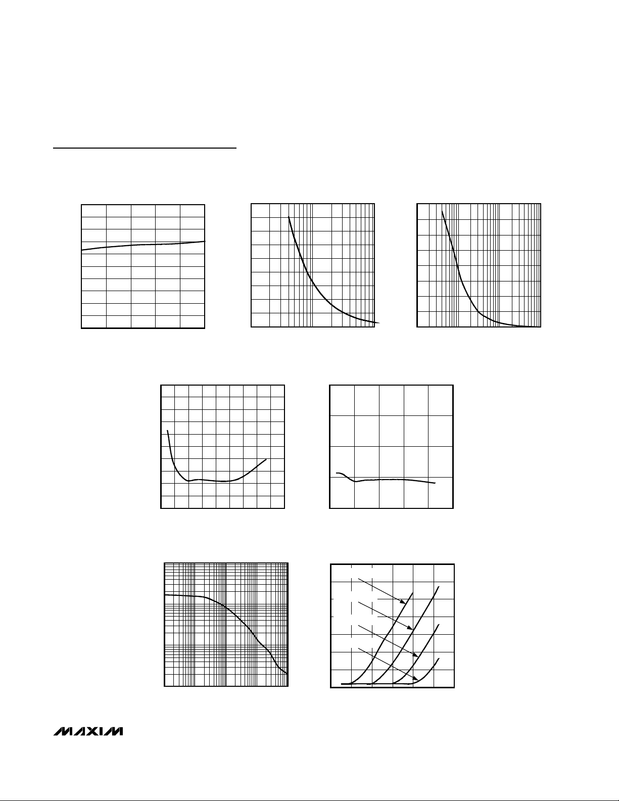
MAX3737
Multirate Laser Driver with Extinction
Ratio Control
200
230
220
210
240
250
260
270
280
290
300
-40 10-15 35 60 85
MODULATION-CURRENT MONITOR GAIN
vs. TEMPERATURE
MAX3737 toc08
TEMPERATURE (°C)
I
MOD
/I
MC_MON
(mA/mA)
90
0
1 10 100
MODULATION CURRENT
vs. R
MODSET
20
10
MAX3737 toc09
R
MODSET
(kΩ)
I
MOD
(mA)
40
30
60
70
50
80
0
15
10
5
20
25
30
35
40
45
50
02010 30 5040 70 8060 90
DETERMINISTIC JITTER
vs. MODULATION CURRENT
MAX3737 toc11
I
MOD
(mA)
DJ
(ps
P-P
)
0
0.5
1.0
1.5
2.0
0 20 40 60 80 100
RANDOM JITTER
vs. MODULATION CURRENT
MAX3737 toc12
I
MOD
(mA)
RJ
(ps
RMS
)
10
0.01
0 0.1 100
COMPENSATION (K)
vs. R
MODBCOMP
0.1
1
MAX3737 toc13
R
MODBCOMP
(kΩ)
K
(mA/mA)
110
30
50
40
60
70
80
90
100
-20 200 40 60 80 100
TEMPERATURE COMPENSATION
vs. R
TH_TEMP
(R
MODCOMP
= 500Ω)
MAX3737 toc14
TEMPERATURE (°C)
I
MOD
(mA)
R
TH_TEMP
= 12kΩ
R
TH_TEMP
= 7kΩ
R
TH_TEMP
= 4kΩ
R
TH_TEMP
= 2kΩ
Typical Operating Characteristics (continued)
(VCC= +3.3V, C
APC
= 0.01µF, I
BIAS
= 20mA, I
MOD
= 30mA, TA = +25°C, unless otherwise noted.)
1.6
0
0.1 10 100
PHOTODIODE CURRENT
vs. R
APCSET
0.4
0.2
0.6
0.8
1.0
1.2
1.4
MAX3737 toc10
R
APCSET
(kΩ)
I
MD
(mA)
1
_______________________________________________________________________________________ 5
Page 6
MAX3737
Multirate Laser Driver with Extinction
Ratio Control
6 _______________________________________________________________________________________
Typical Operating Characteristics (continued)
(VCC= +3.3V, C
APC
= 0.01µF, I
BIAS
= 20mA, I
MOD
= 30mA, TA = +25°C, unless otherwise noted.)
30
32
34
36
38
40
42
44
-20 200 406080100
TEMPERATURE COMPENSATION
vs. R
TH_TEMP
(R
MODTCOMP
= 10kΩ)
MAX3737 toc15
TEMPERATURE (°C)
I
MOD
(mA)
R
TH_TEMP
= 12kΩ
R
TH_TEMP
= 7kΩ
R
TH_TEMP
= 4kΩ
R
TH_TEMP
= 2kΩ
20ms/div
HOT PLUG WITH TX_DISABLE LOW
V
CC
FAULT
MAX3737 toc16
TX_DISABLE
LASER
OUTPUT
t_init = 60ms
3.3V
0V
LOW
LOW
20
µs/div
TRANSMITTER ENABLE
V
CC
FAULT
MAX3737 toc17
TX_DISABLE
LASER
OUTPUT
t_on = 75µs
3.3V
LOW
HIGH
LOW
40ns/div
TRANSMITTER DISABLE
V
CC
FAULT
MAX3737 toc18
TX_DISABLE
LASER
OUTPUT
3.3V
LOW
LOW
t_off = 134ns
HIGH
1µs/div
RESPONSE TO FAULT
V
PC_MON
FAULT
MAX3737 toc19
TX_DISABLE
LASER
OUTPUT
t_fault = 0.9µs
HIGH
EXTERNALLY
FORCED FAULT
LOW
LOW
100ms/div
FAULT RECOVERY TIME
V
PC_MON
FAULT
MAX3737 toc20
TX_DISABLE
LASER
OUTPUT
t_init = 68ms
LOW
EXTERNAL FAULT
REMOVED
LOW
HIGH
HIGH
LOW
Page 7

MAX3737
Multirate Laser Driver with Extinction
Ratio Control
Pin Description
_______________________________________________________________________________________ 7
PIN NAME FUNCTION
1, 10, 15, 16 GND Ground
2 TX_DISABLE
3, 6, 11, 18, 23 V
4 IN+ Noninverted Data Input
5 IN- Inverted Data Input
7 PC_MON
8 BC_MON
9 MC_MON
12 TX_FAULT Open-Collector Transmit Fault Indicator (Table 1)
13 SHUTDOWN
14 VBS
17 BIAS Laser Bias-Current Output
19, 20 OUT-
21, 22 OUT+
24 MD
25 VMD
26 APCFILT1
27 APCFILT2 (See Pin 26.)
28 APCSET A resistor connected from this pin to ground sets the desired average optical power.
29 MODSET
30 MODBCOMP
31 TH_TEMP
32 MODTCOMP
CC
Transmitter Disable, TTL. Laser output is disabled when TX_DISABLE is asserted high or left
unconnected. The laser ouput is enabled when this pin is asserted low.
+3.3V Supply Voltage
Photodiode-Current Monitor Output. Current out of this pin develops a ground-referenced voltage
across an external resistor that is proportional to the monitor-diode current.
Bias-Current Monitor Output. Current out of this pin develops a ground-referenced voltage across
an external resistor that is proportional to the bias current.
Modulation-Current Monitor Output. Current out of this pin develops a ground-referenced voltage
across an external resistor that is proportional to the modulation current amplitude.
Shutdown Driver Output. Voltage output to control an external transistor for optional shutdown
circuitry.
Bias Voltage Sense. Isolated tap (3kΩ ±15%) on the bias output reduces component count when a
precision bias sense resistor is used.
Inverted Modulation-Current Output (Connect Pins 19 and 20 Together). I
when input data is low.
Noninverted Modulation-Current Output (Connect Pins 21 and 22 Together). I
when input data is high.
Monitor Photodiode Input. Connect this pin to the anode of a monitor photodiode. A capacitor to
ground is required to filter the high-speed AC monitor photocurrent.
Monitor Photodiode Voltage Sense. Isolated tap (3kΩ ±15%) on the MD input reduces component
count when a precision photodiode current-sense resistor is used.
Connect a capcitor (C
pole of the APC feedback loop.
A resistor connected from this pin to ground sets the desired constant portion of the modulation
current.
Modulation-Current Compensation from Bias. Couples the bias current to the modulation current.
Mirrors I
Threshold for Temperature Compensation. A resistor at this pin programs the temperature, above
which compensation is added to the modulation current.
Modulation-Current Compensation from Temperature. A resistor at this pin sets the temperature
coefficient of the modulation current when above the threshold temperature. Leave open for zero
temperature compensation.
through an external resistor. Leave open for zero coupling.
BIAS
) between pin 26 (APCFILT1) and pin 27 (APCFILT2) to set the dominant
APC
flows into this pin
MOD
flows into this pin
MOD
EP Exposed Pad
Ground. Solder the exposed pad to the circuit board ground for specified thermal and electrical
performance.
Page 8

MAX3737
Detailed Description
The MAX3737 laser driver consists of three main parts: a
high-speed modulation driver, biasing block with ERC,
and safety circuitry. The circuit design is optimized for
high-speed, low-voltage (+3.3V) operation (Figure 4).
High-Speed Modulation Driver
The output stage is composed of a high-speed differential pair and a programmable modulation current
source. The MAX3737 is optimized for driving a 15Ω
load. The minimum instantaneous voltage required at
OUT+ is 0.7V for modulation current up to 60mA and
0.75V for currents from 60mA to 85mA. Operation
above 60mA can be accomplished by AC-coupling or
with sufficient voltage at the laser to meet the driver
output voltage requirement.
To interface with the laser diode, a damping resistor (RD)
is required. The combined resistance due to the series
damping resistor and the equivalent series resistance
(ESR) of the laser diode should equal 15Ω. To further
damp aberrations caused by laser diode parasitic inductance, an RC shunt network may be necessary. Refer to
Maxim Application Note HFAN 02.0: Interfacing Maxim’s
Laser Drivers to Laser Diodes for more information.
At data rates of 2.7Gbps, any capacitive load at the
cathode of a laser diode degrades optical output performance. Because the BIAS output is directly connected
to the laser cathode, minimize the parasitic capacitance
associated with the pin by using an inductor to isolate
the BIAS pin parasitics from the laser cathode.
Extinction Ratio Control
The extinction ratio (re) is the laser on-state power
divided by the off-state power. Extinction ratio remains
constant if peak-to-peak and average power are held
constant:
P
AVG
+ P
P-P
/ 2P
AVG
- P
P-P
Average power is regulated using APC, which keeps
constant current from a photodiode coupled to the
laser. Peak-to-peak power is maintained by compensating the modulation current for reduced slope efficiency (η) of the laser over time and temperature:
P
P-P
= η x I
MOD
Multirate Laser Driver with Extinction
Ratio Control
8 _______________________________________________________________________________________
,
Figure 1. Required Input Signal and Output Polarity
Figure 2. Test Circuit for Characterization
Figure 3. Supply Filter
V
V
CC
OUT-
OUT-
OUT+
OUT+
CC
30Ω
30Ω
0.5pF
+
I
OUT
VOLTAGE
V
+
IN
-
V
IN
+) - (VIN-)
(V
IN
CURRENT
I
OUT
+
SINGLE ENDED
DIFFERENTIAL
100mV (MIN)
1200mV (MAX)
(MIN)
200mV
P-P
2400mV (MAX)
I
MOD
MAX3737
Z0 = 30Ω
Z0 = 30Ω
30Ω
75Ω
Z0 = 50Ω
50Ω
TIME
HOST BOARD
SOURCE
NOISE
VOLTAGE
SUPPLY
FILTER DEFINED BY SFP MSA
C1
0.1µF
C2
10µF
MODULE
TO LASER
DRIVER V
L1
1µH
C3
0.1µF
OPTIONAL
OPTIONAL
CC
P
AVG
=
ρ
I
MD
MON
OSCILLOSCOPE
Page 9

Modulation compensation from bias increases the modulation current by a user-selected proportion (K) needed to maintain peak-to-peak laser power as bias
current increases with temperature. Refer to Maxim
Application Note HFAN-02.2.1 for details:
This provides a first-order approximation of the current
increase needed to maintain peak-to-peak power. Slope
efficiency decreases more rapidly as temperature
increases. The MAX3737 provides additional temperature compensation as temperature increases past a
user-defined threshold (T
TH
).
Safety Circuitry
The safety circuitry contains a disable, input (TX_DISABLE), a latched fault output (TX_FAULT), and fault
detectors (Figure 5). This circuitry monitors the operation of the laser driver and forces a shutdown if a fault
is detected (Table 1). The TX_FAULT pin should be
pulled high with a 4.7kΩ to 10kΩ resistor to VCCas
required by the SFP MSA. A single-point fault can be a
short to VCCor GND. See Table 2 to view the circuit
response to various single-point failures. The transmit
fault condition is latched until reset by a toggle of
TX_DISABLE or VCC. The laser driver offers redundant
laser diode shutdown through the optional shutdown
circuitry as shown in the Typical Operating Circuit. This
shutdown transistor prevents a single-point fault at the
laser from creating an unsafe condition.
MAX3737
Multirate Laser Driver with Extinction
Ratio Control
Figure 4. Functional Diagram
_______________________________________________________________________________________ 9
R
MDMON
R
BC_MON
R
MC_MON
SHUTDOWN
TX_FAULT
TX_DISABLE
PC_MON
BC_MON
MC_MON
SHUTDOWN
V
CC
MAX3737
R
PULL
INPUT BUFFER
DATA
PATH
I
ENABLE
H
T
R
MOD
I
BIAS
MODTCOMP
ENABLE
xTC
x268 xK
V
BG
R
MODSET
R
SAFETY LOGIC
AND POWER
DETECTOR
= 7.5Ω
I
MD
1
I
BIAS
82
I
MOD
268
V
CC
T > T
TH_TEMP MODTCOMP MODBCOMP APCFILT2MODSET APCFILT1
R
TH_TEMP
MODBCOMP
I
MOD
V
CC
I
BIAS
V
X1/2
C
APC
IN+
IN-
BG
I
APCSET
X1
OUT-
OUT+
BIAS
APCSET
MD
R
APCSET
R
D
I
BIAS
I
MD
C
MD
I
∆
MOD
K
=
I
∆
BIAS
Page 10

MAX3737
Safety Circuitry Current Monitors
The MAX3737 features monitors (MC_MON, BC_MON,
PC_MON) for modulation current (I
MOD
), bias current
(I
BIAS
), and photocurrent (IMD). The monitors are realized
by mirroring a fraction of the currents and developing voltages across external resistors connected to ground.
Voltages greater than V
REF
at MC_MON, PC_MON, or
BC_MON result in a fault state. For example, connecting a
Multirate Laser Driver with Extinction
Ratio Control
10 ______________________________________________________________________________________
Table 1. Typical Fault Conditions
Table 2. Circuit Responses to Various Single-Point Faults
*A fault state asserts the TX_FAULT pin, disables the modulation and bias currents, and asserts the SHUTDOWN pin.
If any of the I/O pins is shorted to GND or V
1
exceed the programmed threshold.
2 End-of-life (EOL) condition of the laser diode. The bias current and/or the photocurrent exceed the programmed threshold.
3 Laser cathode is grounded and photocurrent exceeds the programming threshold.
No feedback for the APC loop (broken interconnection, defective monitor photodiode), and the bias current exceeds the
4
programmed threshold.
(single-point failure; see Table 2), and the bias current or the photocurrent
CC
PIN
TX_FAULT Does not affect laser power. Does not effect laser power.
TX_DISABLE Modulation and bias currents are disabled. Normal condition for circuit operation.
IN+
IN-
MD This disables bias current. A fault state occurs.
SHUTDOWN
BIAS
OUT+
OUT- Does not affect laser power. Does not affect laser power.
PC_MON Fault state* occurs. Does not affect laser power.
BC_MON Fault state* occurs. Does not affect laser power.
MC_MON Fault state* occurs. Does not affect laser power.
APCFILT1
APCFILT2
MODSET Does not affect laser power. Fault state* occurs.
APCSET Does not affect laser power. Fault state* occurs.
CIRCUIT RESPONSE TO OVERVOLTAGE
OR SHORT TO V
The optical average power increases and a fault occurs
if V
PC_MON
responds by decreasing the bias current.
The optical average power decreases and the APC loop
responds by increasing the bias current. A fault state
occurs if V
Does not affect laser power. If the shutdown circuitry is
used, laser current is disabled.
In this condition, laser forward voltage is 0V and no light
is emitted.
The APC circuit responds by increasing the bias current
until a fault is detected, then a fault state* occurs.
I
BIAS
voltage.
I
BIAS
voltage.
exceeds the threshold. The APC loop
exceeds the threshold voltage.
BC_MON
increases until V
increases until V
BC_MON
BC_MON
CC
exceeds the threshold
exceeds the threshold
CIRCUIT RESPONSE TO UNDERVOLTAGE
OR SHORT TO GROUND
The optical average power decreases and the APC loop
responds by increasing the bias current. A fault state
occurs if V
The optical average power increases and a fault occurs
if V
responds by decreasing the bias current.
The APC circuit responds by increasing bias current
until a fault is detected, then a fault* state occurs.
Does not affect laser power.
Fault state* occurs. If the shutdown circuitry is used,
laser current is disabled.
Fault state* occurs. If the shutdown circuitry is used,
laser current is disabled.
I
BIAS
voltage.
I
BIAS
voltage.
BC_MON
PC_MON
increases until V
increases until V
exceeds the threshold voltage.
exceeds the threshold. The APC loop
BC_MON
BC_MON
exceeds the threshold
exceeds the threshold
Page 11

100Ω resistor to ground at each monitor output gives the
following relationships:
V
MC_MON
= (I
MOD
/ 268) ✕ 100Ω
V
BC_MON
= (I
BIAS
/ 82) ✕ 100Ω
V
PC_MON
= I
MD
✕ 100Ω
External sense resistors can be used for high-accuracy
measurement of bias and photodiode currents. On-chip
isolation resistors are included to reduce the number of
components needed to implement this function.
Design Procedure
When designing a laser transmitter, the optical output is
usually expressed in terms of average power and
extinction ratio. Table 3 gives relationships that are
helpful in converting between the optical average
power and the modulation current. These relationships
are valid if the mark density and duty cycle of the optical waveform are 50%.
For a desired laser average optical power (P
AVG
) and
optical extinction ratio (re), the required bias and modulation currents can be calculated using the equations in
Table 3. Proper setting of these currents requires knowl-
edge of the laser to monitor transfer (ρ
MON
) and slope
efficiency (η).
Programming the Monitor Diode Current
Set Point
The MAX3737 operates in APC mode at all times. The
bias current is automatically set so average laser power
is determined by the APCSET resistor:
The APCSET pin controls the set point for the monitordiode current. An internal current regulator establishes
the APCSET current in the same manner as the MODSET
pin. See the I
MD
vs. R
APCSET
graph in the Typical
Operating Characteristics and select the value of R
APC-
SET
that corresponds to the required current at +25°C:
The laser driver automatically adjusts the bias to maintain
the constant average power. For DC-coupled laser diodes:
Programming the Modulation Current with
Compensation
Determine the modulation current from the laser slope
efficiency:
The modulation current of the MAX3737 consists of a
static modulation current (I
MODS
), a current proportional
to I
BIAS,
and a current proportional to temperature. The
portion of I
MOD
set by MODSET is established by an
internal current regulator, which maintains the reference
voltage of V
REF
across the external programming resis-
tor. See to the I
MOD
vs. R
MODSET
graph in the Typical
Operating Characteristics and select the value of R
MOD-
SET
that corresponds to the required current at +25°C:
MAX3737
Multirate Laser Driver with Extinction
Ratio Control
______________________________________________________________________________________ 11
Table 3. Optical Power Relations
Note: Assuming a 50% average input duty cycle and mark density.
P
AVG
I
MD
=
ρ
MON
I
MD
1
=×
2
V
REF
R
APCSET
II
=+
AVG BIAS
I
MOD
2
I
=× ×
2
MOD
Pr
AVG e
η
1
-
+
r
1
e
Average power P
Extinction ratio r
Optical power of a 1 P
Optical power of a zero P
Optical amplitude P
Laser slope efficiency ηη = P
Modulation current I
Threshold current I
Bias current (AC-coupled) I
Laser to monitor transfer ρ
PARAMETER SYMBOL RELATION
AVG
e
1
0
P-P
MOD
TH
BIAS
MON
P
AVG
P1 = 2P
P0 = 2P
P
I
MOD
I
BIAS
= (P0 + P1) / 2
re = P1 / P
AVG re
P-P
P0 at I ≥ I
≥ ITH + I
I
MD
/ (re + 1)
/ (re + 1)
AVG
= P1 - P
/ I
P-P
MOD
= P
P-P
MOD
/ P
AVG
0
0
/ η
TH
/ 2
Page 12

MAX3737
An external resistor at the MODBCOMP pin sets current
proportional to I
BIAS
. Open circuiting the MODBCOMP
pin can turn off the interaction between I
BIAS
and I
MOD
:
If I
MOD
must be increased from I
MOD1
to I
MOD2
to
maintain the extinction ratio at elevated temperature,
the required compensation factor is:
A threshold for additional temperature compensation
can be set with a programming resistor at the
TH_TEMP pin:
The temperature coefficient of thermal compensation
above TTHis set by R
MODTCOMP
. Leaving the MODT-
COMP pin open disables additional thermal compensation:
Current Compliance (I
MOD
≤ 60mA),
DC-Coupled
The minimum voltage at the OUT+ and OUT- pins is
0.7V.
For:
V
DIODE
—Diode bias point voltage (1.2V typ)
R
L
—Diode bias point resistance (5Ω typ)
RD—Series matching resistor (20Ω typ)
For compliance:
Current Compliance (I
MOD
> 60mA),
AC-Coupled
For applications requiring modulation current greater
than 60mA, headroom is insufficient for proper operation of the laser driver if the laser is DC-coupled. To
avoid this problem, the MAX3737’s modulation output
can be AC-coupled to the cathode of a laser diode. An
external pullup inductor is necessary to DC-bias the
modulation output at VCC. Such a configuration isolates
laser forward voltage from the output circuitry and
allows the output at OUT+ to swing above and below
the supply voltage (VCC). When AC-coupled, the
MAX3737 modulation current can be programmed up
to 85mA. Refer to Maxim Application Note HFAN 02.0:
Interfacing Maxim’s Laser Drivers to Laser Diodes for
more information on AC-coupling laser drivers to laser
diodes.
For compliance:
Determine C
APC
The APC loop filter capacitor C
APC
must be selected to
balance the requirements for fast turn-on and minimal
interaction with low frequencies in the data pattern. The
low-frequency cutoff is:
High-frequency noise can be filtered with an additional
cap CMDfrom the MD pin to ground:
The MAX3737 is designed so that turn-on time is faster
than 1ms for most laser gain values (η ✕ ρ
MON
).
Choosing a smaller value of C
APC
reduces turn-on
time. Careful balance between turn-on time and low-frequency cutoff may be needed at low data rates for
some values of laser gain.
Interface Models
Figures 6 and 7 show simplified input and output circuits for the MAX3737 laser driver. If dice are used,
replace package parasitic elements with bondwire parasitic elements.
Multirate Laser Driver with Extinction
Ratio Control
12 ______________________________________________________________________________________
II KII
=+×+
MOD MODS BIAS MODT
V
-
R
MODSET
REF
>
I
=×268
MODS
ITCTTTT
=×
|
MODT TH TH
ITT
=≤
MODT TH
()
|
0
K
±
10%
=
1700
R
+
1000
MODBCOMP
II
MOD MOD
K
=
II
BIAS BIAS
-
21
-
21
I
VV
-
=
OUT C
C
MOD
×+
RR V
()
2
DL+
≥
075 .
TC
=°+
TH
-70
kR
.
92
Ω
.
145
+
M
Ω
TH TEMP
_
°±
C
%
10
TC
=
0510. ()
1
Rk
+°
MODTCOMP
mA
±
%
C
Ω
VVV I RRI R V
- - - .07
=
OUT CC DIODE MOD D L BIAS L+
×+
()
×≥
CF
()
µηρ≈××
APC
68
f kHz
()
3
DB
( )
11
MON
x
C
MD
C
APC
≈
4
Page 13
Layout Considerations
To minimize loss and crosstalk, keep the connections
between the MAX3737 output and the laser diode as
short as possible. Use good high-frequency layout
techniques and multilayer boards with uninterrupted
ground plane to minimize EMI and crosstalk. Circuit
boards should be made using low-loss dielectrics. Use
controlled-impedance lines for data inputs, as well as
the module output.
Laser Safety and IEC 825
Using the MAX3737 laser driver alone does not ensure
that a transmitter design is IEC 825 compliant. The entire
transmitter circuit and component selections must be
considered. Each customer must determine the level of
fault tolerance required by their application, recognizing
that Maxim products are not designed or authorized for
use as components in systems intended for surgical
implant into the body, for applications intended to support
or sustain life, or for any other application where the failure of a Maxim product could create a situation where
personal injury or death may occur.
MAX3737
Multirate Laser Driver with Extinction
Ratio Control
______________________________________________________________________________________ 13
Figure 5. Simplified Safety Circuit
Figure 6. Simplified Input Structure
V
TX_DISABLE
PC_MON
R
PC_MON
BC_MON
R
BC_MON
MC_MON
R
MC_MON
CC
POR AND COUNTER
60ms DELAY
COUNTER
60ms DELAY
V
CC
I
MD
1
V
CC
I
BIAS
82
V
CC
I
MOD
268
EXCESSIVE
MODULATION
CURRENT
MAX3737
I
MOD
ENABLE
100ns
DELAY
V
REF
COMP
V
REF
COMP
V
REF
COMP
RQ
RS
LATCH
S
I
BIAS
ENABLE
CMOS
TTL
OPEN
COLLECTOR
SHUTDOWN
TX_FAULT
MAX3737
PACKAGE
0.83nH
0.11pF
0.83nH
0.11pF
V
CC
V
CC
16kΩ
5kΩ
5kΩ
24kΩ
V
CC
Page 14
MAX3737
Exposed-Pad (EP) Package
The exposed-pad on the 32-pin QFN provides a very low
thermal resistance path for heat removal from the IC. The
pad is also electrical ground on the MAX3737 and should
be soldered to the circuit board ground for proper thermal and electrical performance. Refer to Maxim
Application Note HFAN-08.1: Thermal Considerations for
QFN and Other Exposed Pad Packages at www.maximic.com for additional information.
Multirate Laser Driver with Extinction
Ratio Control
14 ______________________________________________________________________________________
Figure 7. Simplified Output Structure
Pin Configurations (continued)
Chip Information
TRANSISTOR COUNT: 2727
PROCESS: SiGe/Bipolar
V
CC
PACKAGE
0.82nH
0.82nH
0.11pF
0.11pF
OUT-
OUT+
TOP VIEW
APCFILT2
MODTCOMP
TH_TEMP
MODBCOMP
MODSET
32
31
30
29
1GND
TX_DISABLE
PC_MON
BC_MON
2
V
3
CC
IN+
4
9
10
GND
MC_MON
MAX3737ETJ
11
12
CC
V
TX_FAULT
IN-
5
6
V
CC
7
8
5mm x 5mm
THIN QFN
*THE EXPOSED PADDLE MUST BE SOLDERED TO SUPPLY GROUND
TO ACHIEVE SPECIFIED PERFORMANCE.
APCSET
28
27
13
14
VBS
SHUTDOWN
APCFILT1
25 VMD
26
16GND
15
GND
24 MD
23
V
22
OUT+
21
OUT+
20
OUT-
19
OUT-
18
V
BIAS
17
CC
CC
MAX3737
Page 15

MAX3737
Multirate Laser Driver with Extinction
Ratio Control
______________________________________________________________________________________ 15
Typical Operating Circuit
CDR
0.1µF
0.1µF
R
MODBCOMP
R
MODTCOMP
R
TH_TEMP
IN+
IN-
MODBCOMP
MODTCOMP
TH_TEMP
GND
R
MODSET
MODSET
R
APCSET
APCFILT1
APCSET
TX_DISABLE
C
APC
TX_FAULT
MAX3737
APCFILT2
R
MC_MON
+3.3V
CC
V
MC_MON
R
BC_MON
+3.3V
OPTIONAL SHUTDOWN
CIRCUITRY
+3.3V
15Ω
OUT-
SHUTDOWN
BC_MON
R
PC_MON
OUT+
BIAS
MD
PC_MON
10Ω
FERRITE BEAD
C
MD
0.01µF
REPRESENTS A CONTROLLED-IMPEDANCE TRANSMISSION LINE
Page 16

Package Information
(The package drawing(s) in this data sheet may not reflect the most current specifications. For the latest package outline information,
go to www.maxim-ic.com/packages
.)
MAX3737
Multirate Laser Driver with Extinction
Ratio Control
16 ______________________________________________________________________________________
32L QFN.EPS
PACKAGE OUTLINE, 16,20,28,32L QFN,
5x5x0.90 MM
21-0091
PACKAGE OUTLINE, 16,20,28,32L QFN,
5x5x0.90 MM
21-0091
I
I
1
2
2
2
Page 17

MAX3737
Multirate Laser Driver with Extinction
Ratio Control
Maxim cannot assume responsibility for use of any circuitry other than circuitry entirely embodied in a Maxim product. No circuit patent licenses are
implied. Maxim reserves the right to change the circuitry and specifications without notice at any time.
Maxim Integrated Products, 120 San Gabriel Drive, Sunnyvale, CA 94086 408-737-7600 ____________________ 17
© 2003 Maxim Integrated Products Printed USA is a registered trademark of Maxim Integrated Products.
Package Information (continued)
(The package drawing(s) in this data sheet may not reflect the most current specifications. For the latest package outline information,
go to www.maxim-ic.com/packages
.)
PIN # 1
I.D.
D
C
0.15 C A
D/2
0.15
C B
E/2
E
0.10
C
A
0.08 C
A3
A1
(NE-1) X e
DETAIL A
L
D2
k
e
(ND-1) X e
L
e e
PROPRIETARY INFORMATION
TITLE:
PACKAGE OUTLINE
16, 20, 28, 32L, QFN THIN, 5x5x0.8 mm
APPROVAL
C
L
D2/2
b
0.10 M
E2/2
L
DOCUMENT CONTROL NO.
21-0140
C A B
PIN # 1 I.D.
0.35x45
C
E2
L
k
CC
L
REV.
C
L
1
2
QFN THIN.EPS
COMMON DIMENSIONS
NOTES:
1. DIMENSIONING & TOLERANCING CONFORM TO ASME Y14.5M-1994.
2. ALL DIMENSIONS ARE IN MILLIMETERS. ANGLES ARE IN DEGREES.
3. N IS THE TOTAL NUMBER OF TERMINALS.
4. THE TERMINAL #1 IDENTIFIER AND TERMINAL NUMBERING CONVENTION SHALL CONFORM TO JESD 95-1
SPP-012. DETAILS OF TERMINAL #1 IDENTIFIER ARE OPTIONAL, BUT MUST BE LOCATED WITHIN THE
ZONE INDICATED. THE TERMINAL #1 IDENTIFIER MAY BE EITHER A MOLD OR MARKED FEATURE.
5. DIMENSION b APPLIES TO METALLIZED TERMINAL AND IS MEASURED BETWEEN 0.25 mm AND 0.30 mm
FROM TERMINAL TIP.
6. ND AND NE REFER TO THE NUMBER OF TERMINALS ON EACH D AND E SIDE RESPECTIVELY.
7. DEPOPULATION IS POSSIBLE IN A SYMMETRICAL FASHION.
8. COPLANARITY APPLIES TO THE EXPOSED HEAT SINK SLUG AS WELL AS THE TERMINALS.
9. DRAWING CONFORMS TO JEDEC MO220.
10. WARPAGE SHALL NOT EXCEED 0.10 mm.
EXPOSED PAD VARIATIONS
PROPRIETARY INFORMATION
TITLE:
PACKAGE OUTLINE
16, 20, 28, 32L, QFN THIN, 5x5x0.8 mm
21-0140
REV.DOCUMENT CONTROL NO.APPROVAL
2
C
2
 Loading...