

Page 1
General Description
The MAX3679A is a low-jitter precision clock generator
with the integration of three LVPECL and one LVCMOS
outputs optimized for Ethernet applications. The device
integrates a crystal oscillator and a phase-locked loop
(PLL) clock multiplier to generate high-frequency clock
outputs for Ethernet applications.
Maxim’s proprietary PLL design features ultra-low jitter
(0.36ps
RMS
) and excellent power-supply noise rejection,
minimizing design risk for network equipment.
Applications
Ethernet Networking Equipment
Features
♦ Crystal Oscillator Interface: 25MHz
♦ CMOS Input: 25MHz
♦ Output Frequencies for Ethernet
62.5MHz, 125MHz, 156.25MHz, 312.5MHz
♦ Low Jitter
0.14ps
RMS
(1.875MHz to 20MHz)
0.36ps
RMS
(12kHz to 20MHz)
♦ Excellent Power-Supply Noise Rejection
♦ No External Loop Filter Capacitor Required
MAX3679A
+3.3V, Low-Jitter Crystal to LVPECL
Clock Generator
________________________________________________________________
Maxim Integrated Products
1
Ordering Information
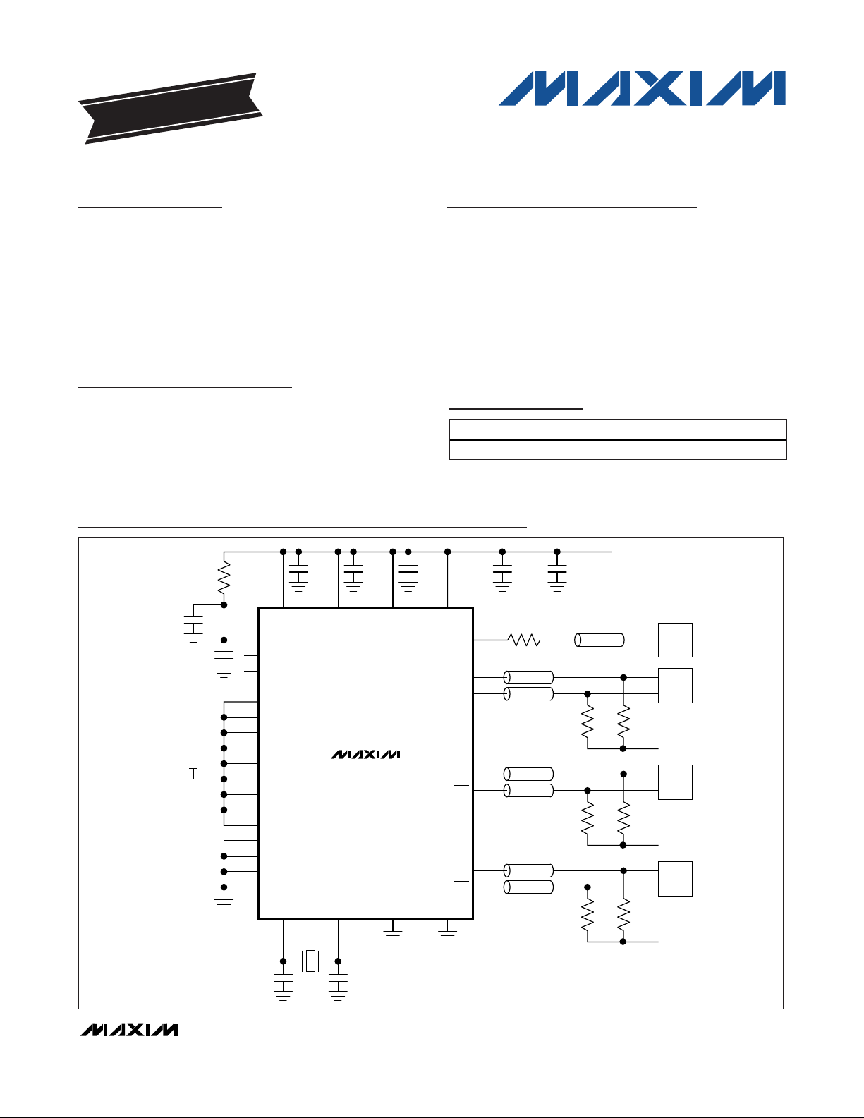
Typical Application Circuit
19-4858; Rev 0; 8/09
For pricing, delivery, and ordering information, please contact Maxim Direct at 1-888-629-4642,
or visit Maxim’s website at www.maxim-ic.com.
+
Denotes a lead(Pb)-free/RoHS-compliant package.
*
EP = Exposed pad.
EVALUATION KIT
AVAILABLE
Pin Configuration appears at end of data sheet.
10.5Ω
PART TEMP RANGE PIN-PACKAGE
MAX3679AETJ+ -40°C to +85°C 32 TQFN-EP*
+3.3V ±5%
0.01μF0.1μF 0.1μF 0.1μF 0.1μF
10μF
0.1μF
V
CC
(C
25MHz
= 18pF)
L
V
CCO_A
MAX3679A
X_IN GNDO_AGND
V
CC
V
CCA
MR
REF_IN
IN_SEL
QAC_OE
QA_OE
QB0_OE
QB1_OE
BYPASS
SELA1
SELA0
SELB1
SELB0
RES1
RES0
X_OUT
33pF 27pF
V
CCO_B
V
DDO_A
QA_C
QB0
QB0
QB1
QB1
QA
QA
125MHz
125MHz
312.5MHz
312.5MHz
36Ω
Z
= 50Ω
0
Z0 = 50Ω
= 50Ω
Z
0
Z0 = 50Ω
Z
= 50Ω
0
Z0 = 50Ω
Z0 = 50Ω
50Ω
50Ω
50Ω
50Ω
50Ω
50Ω
(V
(V
(V
ASIC
ASIC
CC
ASIC
CC
ASIC
CC
- 2V)
- 2V)
- 2V)
Page 2
MAX3679A
+3.3V, Low-Jitter Crystal to LVPECL
Clock Generator
2 _______________________________________________________________________________________
ABSOLUTE MAXIMUM RATINGS
ELECTRICAL CHARACTERISTICS
(VCC= +3.0V to +3.6V, TA= -40°C to +85°C, unless otherwise noted. Typical values are at VCC= +3.3V, TA= +25°C, unless otherwise noted.) (Notes 1, 2, and 3)
Stresses beyond those listed under “Absolute Maximum Ratings” may cause permanent damage to the device. These are stress ratings only, and functional
operation of the device at these or any other conditions beyond those indicated in the operational sections of the specifications is not implied. Exposure to
absolute maximum rating conditions for extended periods may affect device reliability.
Supply Voltage Range VCC, V
CCA
,
V
DDO_A
, V
CCO_A
, V
CCO_B
................................-0.3V to +4.0V
Voltage Range at REF_IN, IN_SEL,
SELA[1:0], SELB[1:0], RES[1:0],
QAC_OE, QA_OE, QB0_OE, QB1_OE,
MR, BYPASS ..........................................-0.3V to (V
CC
+ 0.3V)
Voltage Range at X_IN Pin ...................................-0.3V to +1.2V
Voltage Range at GNDO_A...................................-0.3V to +0.3V
Voltage Range at X_OUT ............................-0.3V to (V
CC
- 0.6V)
Current into QA_C ...........................................................±50mA
Current into QA, QA, QB0, QB0, QB1, QB1 .....................-56mA
Continuous Power Dissipation (T
A
= +70°C)
32-Pin TQFN (derate 34.5mW/°C above +70°C) .......2759mW
Operating Junction Temperature Range...........-55°C to +150°C
Storage Temperature Range .............................-65°C to +160°C
PARAMETER SYMBOL CONDITIONS MIN TYP MAX UNITS
Power-Supply C urrent ICC (Note 4) 77 100 mA
CONTROL INPUT CHARACTERISTICS
(SELA[1:0], SELB[1:0], IN_SEL, QAC_OE, QA_OE, QB1_OE, QB0_OE, MR, BYPASS Pins)
Input Capacitance C
Input Pulldown Resistor R
Input Logic Bia s Resistor R
Input Pullup Resistor R
LVPECL OUTPUT SPECIFICATIONS (QA, QA, QB0, QB0, QB1, QB1 Pins)
Output High Voltage V
Output Low Voltage V
Peak-to-Peak Output-Voltage
Swing (Single-Ended)
Cloc k Output Ris e/Fall Time 20% to 80% (Note 2) 200 350 600 ps
Output Duty-Cycle Distortion
LVCMOS/LVTTL INPUT SPECIFICATIONS
(SELA[1:0], SELB[1:0], IN_SEL, QAC_OE, QA_OE, QB1_OE, QB0_OE, MR, BYPASS Pins)
Input-Voltage High VIH 2.0 V
Input-Voltage Low V
2 pF
IN
PULLDOWN
BIAS
PULLUP
OH
OL
Pin MR 75 k
Pins SELA[1:0], SELB[1:0], QB0_OE 50 k
Pins QAC_OE, QA_OE, QB1_OE, IN_SEL,
BYPASS
TA = 0°C to +85°C
TA = -40°C to 0°C
TA = 0°C to +85°C
TA = -40°C to 0°C
(Note 2) 0.6 0.72 0.9 V
PLL enabled 48 50 52
PLL bypassed (Note 5) 40 50 60
0.8 V
IL
75 k
V
-
CC
1.13
V
CC
1.18
V
CC
1.85
V
CC
1.90
-
-
-
VCC -
0.98
VCC -
1.7
VCC -
0.83
VCC -
0.83
VCC -
1.55
VCC -
1.55
V
V
P-P
%
Page 3
MAX3679A
+3.3V, Low-Jitter Crystal to LVPECL
Clock Generator
_______________________________________________________________________________________ 3
ELECTRICAL CHARACTERISTICS (continued)
(VCC= +3.0V to +3.6V, TA= -40°C to +85°C, unless otherwise noted. Typical values are at VCC= +3.3V, TA= +25°C, unless otherwise noted.) (Notes 1, 2, and 3)
Note 1: A series resistor of up to 10.5Ω is allowed between VCCand V
CCA
for filtering supply noise when system power-supply
tolerance is V
CC
= 3.3V ±5%. See Figure 2.
PARAMETER SYMBOL CONDITIONS MIN TYP MAX UNITS
Input High Current I
Input Low Current I
REF_IN SPECIFICATIONS (Input DC- or AC-Coupled)
Reference Clock Frequenc y
Input-Voltage High VIH 2.0 V
Input-Voltage Low V
Input High Current I
Input Low Current I
Reference Clock Duty Cycle PLL enab led 30 70 %
Input Capacitance 2.5 pF
QA_C SPECIFICATIONS
Output High Voltage VOH QA_C sourcing 12mA 2.6 V
Output Low Voltage V
Output Rise/Fall Time (Notes 3, 6) 250 500 1000 ps
Output Duty-Cycle Distortion
Output Impedance 14
CLOCK OUTPUT AC SPECIFICATIONS
VCO Frequency Range 625 MHz
Random Jitter (Note 7) RJ
Deterministic Jitter Due to
Supply Noise
Spurs Induced by Power-Supply
Noise (Note s 7, 9, 10)
Nonharmonic and Subharmonic
Spurs
Output Skew
Clock Output SSB Phase Noise
at 125MH z (Note 11)
IH
IL
IH
IL
OL
RMS
VIN = V
CC
VIN = 0V -80 μA
PLL enabled 25
PLL bypassed 320
0.8 V
IL
VIN = V
CC
VIN = 0V -240 μA
QA_C sink ing 12mA 0.4 V
PLL enabled 42 50 58
PLL bypassed (Note 5) 40 60
12kHz to 20MHz 0.36 1.0
1.875MHz to 20MHz 0.14
LVPECL o utput (Notes 7, 8, 9) 5.0 ps
LVPECL o utput -59
LVCMOS output -47
-70 dBc
Between QB0 and QB1 15
Between QA and QB0 or QB1,
PECL outputs
f = 1kHz -124
f = 10kHz -125
f = 100kHz -130
f = 1MHz -145
f > 10MH z -153
80 μA
MHz
240 μA
%
ps
RMS
P-P
dBc
20
ps
dBc/Hz
Page 4
MAX3679A
+3.3V, Low-Jitter Crystal to LVPECL
Clock Generator
4 _______________________________________________________________________________________
ELECTRICAL CHARACTERISTICS (continued)
(VCC= +3.0V to +3.6V, TA= -40°C to +85°C, unless otherwise noted. Typical values are at VCC= +3.3V, TA= +25°C, unless otherwise noted.) (Notes 1, 2, and 3)
Figure 1. LVCMOS Output Measurement Setup
Note 2: Guaranteed up to 320MHz for LVPECL output.
Note 3: Guaranteed up to 160MHz for LVCMOS output.
Note 4: All outputs enabled and unloaded. IN_SEL set high.
Note 5: Measured with crystal or AC-coupled, 50% duty-cycle signal on REF_IN.
Note 6: Measured using setup shown in Figure 1 with V
CC
= 3.3V ±5%.
Note 7: Measured with crystal source.
Note 8: Total TIE including random and deterministic jitter. Measured with Agilent DSO81304A 40GS/s real-time oscilloscope
using 2M sample record length.
Note 9: Measured with 40mV
P-P
, 100kHz sinusoidal signal on the supply.
Note 10: Measured at 156.25MHz output.
Note 11: Measured with 25MHz crystal or 25MHz reference clock at LVCMOS input with a slew rate of 0.5V/ns or greater.
MAX3679A
QA_C
36Ω 499Ω
4.7pF
0.1μF
OSCILLOSCOPE
Z0 = 50Ω
50Ω
Page 5

MAX3679A
+3.3V, Low-Jitter Crystal to LVPECL
Clock Generator
_______________________________________________________________________________________
5
Typical Operating Characteristics
(Typical values are at VCC= +3.3V, TA= +25°C, crystal frequency = 25MHz.)
SUPPLY CURRENT
vs. TEMPERATURE
MAX3679A toc01
AMBIENT TEMPERATURE (°C)
SUPPLY CURRENT (mA)
603510-15
25
50
75
100
125
150
175
200
225
250
0
-40 85
ALL OUTPUTS ACTIVE AND TERMINATED
ALL OUTPUTS ACTIVE AND UNTERMINATED
OUTPUT WAVEFORM AT 125MHz
(LVCMOS OUTPUT)
MAX3679A toc03
1ns/div
AMPLITUDE (50mV/div)
MEASURED USING 50Ω OSCILLOSCOPE INPUT
THROUGH NETWORK SHOWN IN FIGURE 1
PHASE NOISE AT 312.5MHz
CLOCK FREQUENCY
MAX3679A toc04
OFFSET FREQUENCY (kHz)
NOISE POWER DENSITY (dBc/Hz)
10,00010001 10 100
-150
-140
-130
-120
-110
-100
-90
-80
-160
0.1 100,000
PHASE NOISE AT 125MHz
CLOCK FREQUENCY
MAX3679A toc05
OFFSET FREQUENCY (kHz)
NOISE POWER DENSITY (dBc/Hz)
10,00010001 10 100
-150
-140
-130
-120
-110
-100
-90
-80
-160
0.1 100,000
DIFFERENTIAL OUTPUT WAVEFORM
AT 156.25MHz (LVPECL OUTPUT)
AMPLITUDE (200mV/div)
1ns/div
MAX3679A toc02
JITTER HISTOGRAM (312.5MHz OUTPUT,
SUPPLY NOISE AT 100kHz)
40mV
P-P
DJ = 5.0ps
5ps/div
MAX3679A toc06
P-P
0
-10
-20
-30
-40
-50
-60
SPUR AMPLITUDE (dBc)
-70
-80
-90
NOISE SPUR AMPLITUDE
vs. NOISE FREQUENCY
fC = 156.25MHz
NOISE AMPLITUDE = 40mV
10 10,000
NOISE FREQUENCY (kHz)
P-P
1000100
MAX3679A toc07
Page 6

MAX3679A
+3.3V, Low-Jitter Crystal to LVPECL
Clock Generator
6 _______________________________________________________________________________________
Pin Description
PIN NAME FUNCTION
1 V
2, 19, 24 GND Supply Ground
3 QB0_OE
4, 5
6 QAC_OE
7 MR
8 GNDO_A Ground for QA_C Output. Connect to supply ground.
9 QA_C LVCMOS Clock Output
10 V
11 V
12 QA Noninverting Clock Output, LVPECL
13 QA Inverting Clock Output, LVPECL
14 BYPASS
15 RES1 Not Internally Connected. Connect to GND, VCC, or leave open for normal operation.
16 RES0 Reserved for Test. Connect to GND for normal operation.
17 V
18 VCC Core Power Supply. Connect to +3.3V.
20 QA_OE
21, 22
23 QB1_OE
25 X_OUT Crysta l Oscillator Output
26 X_IN Crystal Oscillator Input
27 REF_IN LVCMOS Reference Clock Input. Self-biased to allow AC- or DC-coupling.
28 IN_SEL
29 QB1 LVPECL, Inverting C lock Output
30 QB1 LVPECL, Nonin verting Clock Output
31 QB0 LVPECL, Inverting C lock Output
32 QB0 LVPECL, Nonin verting Clock Output
— EP Exposed Pad. Connect to supply ground for proper electrical and therma l performance.
Power Supply for QB0 and QB1 Clock Outputs. Connect to +3.3V.
CCO_ B
LVCMOS/LVTTL Input. Enables/disables QB0 clock output. Connect pin high to enable LVPECL
clock output QB0. Connect low to set QB0 to a logic 0. Has internal 50k input impedance.
SELB1 ,
SELB0
DDO_ A
CCO_ A
CCA
SELA0 ,
SELA1
LVCMOS/LVTTL Input. Controls NB divider setting. Has 50k input impedance. See Table 2 for
more information.
LVCMOS/LVTTL Input. Enables/disables QA_C clock output. Connect pin hi gh to enable QA_C.
Connect low to set QA_C to a high-impedance state. Ha s internal 75k pullup to V
LVCMOS/LVTTL Input. Master reset input. Pulse high for > 1μ s to reset al l dividers. Has internal
75k pulldown to GND. Not required for normal operation.
Power Supply for QA_C Clock Output. Connect to +3.3V.
Power Supply for QA Clock Output. Connect to +3.3V.
LVCMOS/LVTTL Input (Active Low). Connect low to bypass the internal PLL. Connect high for
normal operation. When in bypass mode the output div iders are set to divide by 1. Has internal
75k pullup to V
Analog Power Supply for the VCO. Connect to +3.3V. For additional power-supply noise f iltering,
this pin can connect to V
LVCMOS/LVTTL Input. Enables/disables the QA clock output. Connect this p in high to enable the
LVPECL c lock output QA. Con nect low to set QA t o a logic 0. Ha s internal 75k pullup to V
LVCMOS/LVTTL Input. Controls NA d ivider setting. See Table 2 for more information. Has 50k
input impedance.
LVCMOS/LVTTL Input. Enables/disables QB1 clock output. Connect pin high to enable LVPECL
clock output QB1. Connect low to set QB1 to a logic 0. Has internal 50k input impedance.
LVCMOS/LVTTL Input. Connect high or leave open to use a crystal. Connect low to use REF_IN.
Has internal 75k pullup to V
CC
.
through 10.5 as shown in Figure 2 (requires VCC = +3.3V ±5%).
CC
.
CC
.
CC
.
CC
Page 7
MAX3679A
Detailed Description
The MAX3679A is a low-jitter clock generator designed
to operate at Ethernet frequencies. It consists of an onchip crystal oscillator, PLL, programmable dividers,
LVCMOS output buffer, and LVPECL output buffers.
Using a low-frequency clock (crystal or CMOS input) as
a reference, the internal PLL generates a high-frequency output clock with excellent jitter performance.
Crystal Oscillator
An integrated oscillator provides the low-frequency
reference clock for the PLL. This oscillator requires an
external crystal connected between X_IN and X_OUT.
Crystal frequency is 25MHz.
REF_IN Buffer
An LVCMOS-compatible clock source can be connected
to REF_IN to serve as the reference clock.
The LVCMOS REF_IN buffer is internally biased to allow
AC- or DC-coupling. It is designed to operate up to
320MHz.
PLL
The PLL takes the signal from the crystal oscillator or
reference clock input and synthesizes a low-jitter, highfrequency clock. The PLL contains a phase-frequency
detector (PFD), a lowpass filter, and a 625MHz voltagecontrolled oscillator (VCO). The VCO output is connected to the PFD input through a feedback divider. The
PFD compares the reference frequency to the divideddown VCO output (f
VCO
/25) and generates a control
signal that keeps the VCO locked to the reference
clock. The high-frequency VCO output clock is sent to
the output dividers. To minimize noise-induced jitter,
the VCO supply (V
CCA
) is isolated from the core logic
and output buffer supplies.
Output Dividers
The output divider is programmable to allow a range of
output frequencies. See Table 2 for the divider input
settings. The output dividers are automatically set to
divide by 1 when the MAX3679A is in bypass mode
(BYPASS = 0).
LVPECL Drivers
The high-frequency outputs—QA, QB0, and QB1—are
differential PECL buffers designed to drive transmission
lines terminated with 50Ω to VCC- 2.0V. The maximum
operating frequency is specified up to 320MHz. Each
output can be individually disabled, if not used. The
outputs go to a logic 0 when disabled.
LVCMOS Driver
QA_C, the LVCMOS output, is designed to drive a single-ended high-impedance load. The maximum operating frequency is specified up to 160MHz. This output
can be disabled by the QAC_OE pin if not used and
goes to a high impedance when disabled.
Reset Logic/POR
During power-on, the power-on reset (POR) signal is
generated to synchronize all dividers. An external master reset (MR) signal is not required.
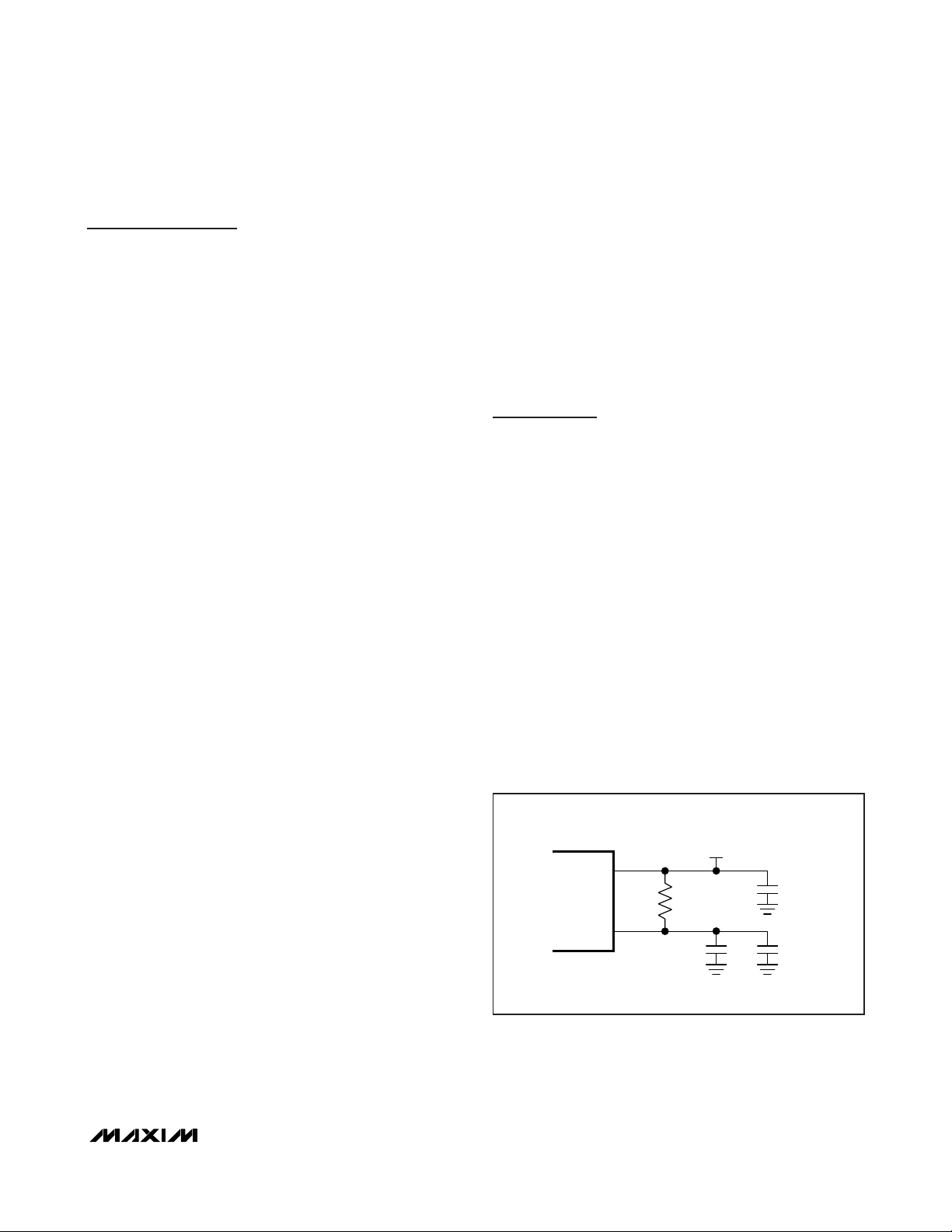
Applications Information
Power-Supply Filtering
The MAX3679A is a mixed analog/digital IC. The PLL
contains analog circuitry susceptible to random noise.
In addition to excellent on-chip power-supply noise
rejection, the MAX3679A provides a separate powersupply pin, V
CCA
, for the VCO circuitry. Figure 2 illustrates the recommended power-supply filter network for
V
CCA
. The purpose of this design technique is to
ensure clean input power supply to the VCO circuitry
and to improve the overall immunity to power-supply
noise. This network requires that the power supply is
+3.3V ±5%. Decoupling capacitors should be used on
all other supply pins for best performance.
Output Divider Configuration
Table 2 shows the input settings required to set the output dividers. Leakage in the OPEN case must be less
than 1µA. Note that when the MAX3679A is in bypass
mode (BYPASS set low), the output dividers are automatically set to divide by 1.
Figure 2. Analog Supply Filtering
+3.3V, Low-Jitter Crystal to LVPECL
Clock Generator
_______________________________________________________________________________________ 7
V
CC
V
CCA
10.5Ω
+3.3V ±5%
0.1μF
0.1μF 10μF
Page 8

MAX3679A
+3.3V, Low-Jitter Crystal to LVPECL
Clock Generator
8 _______________________________________________________________________________________
Crystal Selection
The crystal oscillator is designed to drive a fundamental
mode, AT-cut crystal resonator. See Table 3 for recommended crystal specifications. See Figure 4 for external
capacitance connection.
Crystal Input Layout and
Frequency Stability
The crystal, trace, and two external capacitors should
be placed on the board as close as possible to the
MAX3679A’s X_IN and X_OUT pins to reduce crosstalk
of active signals into the oscillator.
The layout shown in Figure 3 gives approximately 3pF
of trace plus footprint capacitors per side of the crystal
(Y1). The dielectric material is FR4 and dielectric thickness of the reference board is 15 mils. Using a 25MHz
crystal and the capacitor values of C22 = 27pF and
C23 = 33pF, the measured output frequency accuracy
is -14ppm at +25°C ambient temperature.
Table 2. Output Divider Configuration
Table 3. Crystal Selection Parameters
Table 1. Output Frequency Determination
*Maximum guaranteed output frequency is 160MHz for CMOS
and 320MHz for LVPECL output.
Figure 3. Crystal Layout
Figure 4. Crystal, Capacitors Connection
XO OR CMOS
INPUT
FREQUENCY
(MHz)
25 25 625
FEEDBACK
DIVIDER, M
VCO
FREQUENCY
(MHz)
OUTPUT
DIVIDER,
NA AND NB
÷2 312.5
÷4 156.25
÷5 125
÷10 62.5
OUTPUT
FREQUENCY
(MHz)
APPLICATIONS
Ethernet
INPUT
SELA1/SELB1 SELA0/SELB0
0 0 ÷2*
1 0 ÷4
1 1 ÷5
0 OPEN ÷10
NA/NB DIVIDER
PARAMETER SYMBOL MIN TYP MAX UNITS
Crystal Oscillation
Frequency
Shunt Capacitance CO 2.0 7.0 pF
Load Capacitance CL 18 pF
Equivalent Series
Resistance (ESR)
Maximum Crystal
Dri ve Le ve l
25MHz CRYSTAL
f
25 MHz
OSC
R
50
S
300 μW
27pF
X_IN
= 18pF)
(C
L
X_OUT
33pF
Page 9

MAX3679A
_______________________________________________________________________________________ 9
+3.3V, Low-Jitter Crystal to LVPECL
Clock Generator
Interfacing with LVPECL Outputs
The equivalent LVPECL output circuit is given in Figure 8.
These outputs are designed to drive a pair of 50Ω transmission lines terminated with 50Ω to V
TT=VCC
- 2V. If a
separate termination voltage (V
TT
) is not available, other
termination methods can be used such as shown in
Figures 5 and 6. Unused outputs should be disabled and
can be left open. For more information on LVPECL terminations and how to interface with other logic families,
refer to Application Note 291:
HFAN-01.0: Introduction to
LVDS, PECL, and CML
.
Interface Models
Figures 7, 8, and 9 show examples of interface models.
Figure 5. Thevenin Equivalent of Standard PECL Termination
Figure 6. AC-Coupled PECL Termination
Figure 7. Simplified REF_IN Pin Circuit Schematic
Figure 8. Simplified LVPECL Output Circuit Schematic
Figure 9. Simplified LVCMOS Output Circuit Schematic
130Ω 130Ω
MAX3679A
Z
Qx
Qx
= 50Ω
0
Z0 = 50Ω
82Ω
+3.3V
82Ω
0.1μF
0.1μF
Z0 = 50Ω
100Ω
Z0 = 50Ω
Qx
MAX3679A
Qx
HIGH
IMPEDANCE
HIGH
IMPEDANCE
V
CC
Qx
Qx
ESD
STRUCTURES
150Ω
150Ω
NOTE: AC-COUPLING IS OPTIONAL.
V
CC
V
= 1.4V
B
V
REF_IN
CC
V
B
14.5kΩ
ESD
STRUCTURES
V
DDO_A
DISABLE
10Ω
QA_CIN
V
B
10Ω
ESD
STRUCTURES
Page 10

MAX3679A
+3.3V, Low-Jitter Crystal to LVPECL
Clock Generator
10 ______________________________________________________________________________________
×
Pin Configuration
Layout Considerations
The inputs and outputs are critical paths for the
MAX3679A, and care should be taken to minimize discontinuities on these transmission line. Here are some
suggestions for maximizing the MAX3679A’s performance:
• An uninterrupted ground plane should be positioned beneath the clock I/Os.
• Ground pin vias should be placed close to the IC
and the input/output interfaces to allow a return
current path to the MAX3679A and the receive
devices.
• Supply decoupling capacitors should be placed
close to the MAX3679A supply pins.
• Maintain 100Ω differential (or 50Ω single-ended)
transmission line impedance out of the MAX3679A.
• Use good high-frequency layout techniques and a
multilayer board with an uninterrupted ground
plane to minimize EMI and crosstalk.
Refer to the MAX3679A Evaluation Kit for more information.
Exposed-Pad Package
The exposed pad on the 32-pin TQFN package provides a very low inductance path for return current traveling to the PCB ground plane. The pad is also
electrical ground on the MAX3679A and must be soldered to the circuit board ground for proper electrical
performance.
Chip Information
TRANSISTOR COUNT: 10,780
PROCESS: BiCMOS
TOP VIEW
V
1
CCO_B
GND
2
SELB1
SELB0
MR
3
4
5
6
7
8
910
QB0_OE
QAC_OE
GNDO_A
*EXPOSED PAD CONNECTED TO GROUND.
QB1
QB0
QB0
3132 30 28 27 26
QB1
29
+
MAX3679A
*EP
12 13 14 15
11
DDO_A
CCO_A
V
V
THIN QFN
(5mm
QA
QA_C
IN_SEL
QA
5mm)
REF_IN
BYPASS
X_IN
RES1
25
16
X_OUT
24
23
22
21
20
19
18
17
RES0
GND
QB1_OE
SELA1
SELA0
QA_OE
GND
V
CC
V
CCA
Page 11

MAX3679A
+3.3V, Low-Jitter Crystal to
LVPECL Clock Generator
Maxim cannot assume responsibility for use of any circuitry other than circuitry entirely embodied in a Maxim product. No circuit patent licenses are
implied. Maxim reserves the right to change the circuitry and specifications without notice at any time.
Maxim Integrated Products, 120 San Gabriel Drive, Sunnyvale, CA 94086 408-737-7600 ____________________
11
© 2009 Maxim Integrated Products Maxim is a registered trademark of Maxim Integrated Products, Inc.
CRYSTAL
OSCILLATOR
LVCMOS
DIVIDERS:
NA = 2, 4, 5, 10
NB = 2, 4, 5, 10
REF_IN
X_IN
25MHz
X_OUT
0
1
0
1
PFD FILTER
÷25
DIVIDER
NB
DIVIDER
NA
VCO
625MHz
LVCMOS
BUFFER
QA_C
QAC_OE
LVPECL
BUFFER
QA
QA_OE
QA
LVPECL
BUFFER
QB1
QB1_OE
QB1
LVPECL
BUFFER
QB0
QB0_OE
QB0
SELB[1:0]
SELA[1:0]IN_SEL
BYPASS
MAX3679A
33pF
27pF
Block Diagram
PACKAGE TYPE PACKAGE CODE DOCUMENT NO.
32 TQFN-EP T3255+3
21-0140
Package Information
For the latest package outline information and land patterns, go to www.maxim-ic.com/packages.
 Loading...