

Page 1
MAX3673
Low-Jitter Frequency Synthesizer
with Selectable Input Reference
________________________________________________________________
Maxim Integrated Products
1
19-4442; Rev 0; 2/09
For pricing, delivery, and ordering information, please contact Maxim Direct at 1-888-629-4642,
or visit Maxim’s website at www.maxim-ic.com.
EVALUATION KIT
AVAILABLE
General Description
The MAX3673 is a low-jitter frequency synthesizer that
accepts two reference clock inputs and generates nine
phase-aligned outputs. The device features 40kHz jitter
transfer bandwidth, 0.3ps
RMS
(12kHz to 20MHz) integrated phase jitter, and best-in-class power-supply
noise rejection (PSNR), making it ideal for jitter cleanup, frequency translation, and clock distribution in wireless base-station applications.
The MAX3673 operates from a single +3.3V supply and
typically consumes 400mW. The IC is available in an
8mm x 8mm, 56-pin TQFN package, and operates from
-40°C to +85°C.
Applications
3G Wireless Base Stations
Frequency Translation
Jitter Cleanup
Clock Distribution
Features
♦ Two Reference Clock Inputs: LVPECL
♦ Nine Phase-Aligned Clock Outputs: LVPECL
♦ Input Frequencies: 61.44MHz,122.88MHz,
245.76MHz, 307.2MHz
♦ Output Frequencies: 61.44MHz, 122.88MHz,
153.6MHz, 245.76MHz, 307.2MHz
♦ Low-Jitter Generation: 0.3ps
RMS
(12kHz to 20MHz)
♦ Clock Failure Indicator for Both Reference Clocks
♦ External Feedback Provides Zero-Delay Capability
♦ Low Output Skew: 20ps Typical
Ordering Information
PART TEMP RANGE PIN-PACKAGE
MAX3673ETN+ -40°C to +85°C 56 TQFN-EP*
SIGNAL QUALIFIER
AND
LOCK DETECT
POWER-ON
RESET
(POR)
IN0FAIL
IN1FAIL
LOCK
REFCLK0
REFCLK0
FB_INFB_SEL FB_IN
REFCLK1
REFCLK1
MR
0
1
1
0
DIV M
DMSEL_CLK
DA
DB
PFD CP
DIV N
DIV A
DIV B
VCO
2.457GHz61.44MHz
OUTA2
OUTA2
OUTA1
OUTA1
OUTA3
OUTA3
OUTA0
OUTB_EN
OUTA0
OUTA_ENPLL_BYPASS
1
0
10
OUTB3
OUTB3
OUTB2
OUTB2
OUTB4
OUTB4
OUTB1
OUTB1
OUTB0
OUTB0
C
PLL
0.1μF
C
REG
0.22μF
MAX3673
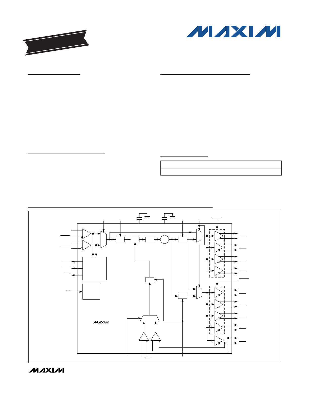
Functional Diagram
+
Denotes a lead(Pb)-free/RoHS-compliant package.
*
EP = Exposed pad.
Pin Configuration and Typical Application Circuits appear at
end of data sheet.
Page 2
MAX3673
Low-Jitter Frequency Synthesizer
with Selectable Input Reference
2 _______________________________________________________________________________________
ABSOLUTE MAXIMUM RATINGS
ELECTRICAL CHARACTERISTICS
(VCC= +3.0V to +3.6V, TA= -40°C to +85°C, C
PLL
= 0.1µF, C
REG
= 0.22µF. Typical values are at VCC= +3.3V, TA= +25°C, unless
otherwise noted.)
Stresses beyond those listed under “Absolute Maximum Ratings” may cause permanent damage to the device. These are stress ratings only, and functional
operation of the device at these or any other conditions beyond those indicated in the operational sections of the specifications is not implied. Exposure to
absolute maximum rating conditions for extended periods may affect device reliability.
Supply Voltage Range (VCC, VCC_VCO)..............-0.3V to +4.0V
LVPECL Output Current (OUTA[3:0],
, OUTB[4:0], ) .............................-56mA
All Other Pins..............................................-0.3V to (V
CC
+ 0.3V)
Continuous Power Dissipation (T
A
= +70°C)
56-Pin TQFN (derate 47.6mW/°C above 70°C)..........3808mW
Operating Junction Temperature (T
J
)................-55°C to +150°C
Storage Temperature Range .............................-65°C to +160°C
Lead Temperature (soldering, 10s) .................................+300°C
O
UTA[ : ]30
OUTB[ : ]40
Supply Current ICC LVPECL outputs unt ermin ated 120 175 mA
POWER-ON RESET
VCC Rising (Note 1) 2.55 V
VCC Falling (Note 1) 2.45 V
LVCMOS/LVTTL INPUTS (MR, SEL_CLK, PLL_BYPAS S, FB_SEL)
Input High Voltage VIH 2.0 V
Input Low Voltage VIL 0.8 V
Input High Current IIH VIN = VCC 75 μA
Input Low Current IIL VIN = GND -75 μA
LVCMOS/LVTTL OUTPUTS (IN0FAIL, IN1FAIL, LOCK)
Output High Voltage VOH IOH = -8mA 2.4 V
Output Low Voltage VOL IOL = +8mA 0.4 V
LVPECL INPUTS (REFCLK0, REFCLK0, REFCLK1, REFCLK1, FB_IN, FB_IN) (Note 2)
Input High Voltage VIH
Input Low Voltage V
Input Bias Voltage V
Differentia l-Input Swing 0.15 1.9 V
Differentia l-Input Impedance > 40 k
Common-Mode Input Impedance > 14 k
Input Capacitance 1.5 pF
Input Current VIH = VCC - 0.7V, VIL = VCC - 2.0V -100 +100 μA
Input Inrush Current When Power
is Off (Steady State)
Input Inrush Current Over shoot
When Power i s Off
PARAMETER SYMBOL CONDITIONS MIN TYP MAX UNITS
IL
CMI
I
DC
I
OVERSHOOT
(Notes 3, 4) 8 mA
(Notes 3, 4) 6 mA
VCC -
2.0
VCC -
1.8
V
VCC -
1.34
V
-
CC
0.7
V
V
P-P
Page 3
MAX3673
Low-Jitter Frequency Synthesizer
with Selectable Input Reference
_______________________________________________________________________________________ 3
ELECTRICAL CHARACTERISTICS (continued)
(VCC= +3.0V to +3.6V, TA= -40°C to +85°C, C
PLL
= 0.1µF, C
REG
= 0.22µF. Typical values are at VCC= +3.3V, TA= +25°C, unless
otherwise noted.)
REFERENCE CLOCK INPUTS (REFCLK0, REFCLK0, REFCLK1, REFCLK1)
Reference Clock Frequenc y f
Reference Clock Frequenc y
Tolerance
Reference Clock Duty Cycle 40 60 %
Reference Clock Amplitude
Detection Assert Threshold
LVPECL OUTPUTS (OUTA[3:0],
Output High Voltage V
Output Low Voltage V
Differentia l-Output Swing 1.1 1.45 1.8 V
Output Current When Disabled VO = VCC - 2.0V to VCC - 0.7V 130 μA
Output Frequency f
Output Rise/Fall Time tR, tF 20% to 80% (Note 8) 150 500 ps
Output Duty Cycle
Output-to-Output Skew t
OTHER AC ELECTRICAL SPECIFICATIONS
PLL Jitter Transfer Bandwidth 40 kH z
Jitter Peaking 0.1 dB
PFD Compare Frequency 61.44 MHz
VCO Center Frequency 2.457 GHz
Random Jitter Generation Integrated 12kH z to 20MH z (Notes 5, 8) 0.3 1.0 ps
Determinisitic Jitter Caused by
Power-Supply Noise
PARAMETER SYMBOL CONDITIONS MIN TYP MAX UNITS
REF
-200 +200 ppm
V
DT
OUTA[3:0],
OH
OL
OUT
SKEW
(Note 10) 5 ps
Table 1 MHz
Differentia l swing (Notes 5, 6) 200 mV
OUTB[4:0],
OUTB[4:0])
PLL_BYP ASS = 0 48 52
PLL_BYP ASS = 1 (Note 9) 45 55
Within output bank 20
All outputs 40
(Note 7)
VCC -
1.13
VCC -
1.85
VCC -
0.98
VCC -
1.70
Table s
2, 3
VCC -
0.83
VCC -
1.55
MHz
P-P
V
V
P-P
%
ps
RMS
P-P
Frequency Difference Between
Reference Clock and VCO
Within Which the PLL i s
Considered in Lock
Frequency Difference Between
Reference Clock and VCO at
Which the PLL is Con sidered
Out-of-Lock
PLL Lock Time t
500 ppm
800 ppm
Figure 2 600 μs
LOCK
Page 4
MAX3673
Low-Jitter Frequency Synthesizer
with Selectable Input Reference
4 _______________________________________________________________________________________
ELECTRICAL CHARACTERISTICS (continued)
(VCC= +3.0V to +3.6V, TA= -40°C to +85°C, C
PLL
= 0.1µF, C
REG
= 0.22µF. Typical values are at VCC= +3.3V, TA= +25°C, unless
otherwise noted.)
Note 1: During the power-on-reset time, the LVPECL outputs are held to logic-low (OUTxx = low, OUTxx = high). See the
Power-
On-Reset (POR)
section for more information.
Note 2: LVPECL inputs can be AC- or DC-coupled.
Note 3: For hot-pluggable purposes, the device can receive LVPECL inputs when no supply voltage is applied. Measured with
V
CC
pins connected to GND. See Figure 1.
Note 4: Measured with LVPECL input (V
IH
, VIL) as specified.
Note 5: Measured using reference clock input with 550ps rise/fall time (20% to 80%).
Note 6: When input differential swing is below the specified threshold, a clock failure is declared. See Figure 4.
Note 7: LVPECL outputs terminated 50Ω to V
TT
= VCC- 2V.
Note 8: Guaranteed by design and characterization.
Note 9: Measured with 50% duty cycle at reference clock input.
Note 10: Measured with 50mV
P-P
sinusoidal noise on the power supply, f
NOISE
= 100kHz.
Note 11: Measured with f
REFCLKx
= f
FB_IN
and matched slew rates.
Master Reset (MR) Minimum
Pulse Width
Propagation Delay from Input to
FB_IN
Propagation Delay from Input to
Any Output
PARAMETER SYMBOL CONDITIONS MIN TYP MAX UNITS
100 ns
FB_SEL = 1 (Notes 8, 11) -120 +120 ps
PLL_BYP ASS = 1 1.0 ns
Page 5
MAX3673
Low-Jitter Frequency Synthesizer
with Selectable Input Reference
_______________________________________________________________________________________ 5
Figure 1. LVPECL Input Inrush Current
REFCLK0
REFCLK1
OUTxx
IN0FAIL
IN1FAIL
LOCK
HIGH
SEL_CLK
LOW
V
CC
POWER-ON-RESET (~ 20μs)
HIGH
t
LOCK
(~ 600μs)
PLL LOCKED TO REFCLK0
Figure 2. Power-Up, PLL Locks to REFCLK0
INRUSH CURRENT
(mA)
I
OVERSHOOT
I
DC
t
Page 6

MAX3673
Low-Jitter Frequency Synthesizer
with Selectable Input Reference
6 _______________________________________________________________________________________
Typical Operating Characteristics
(VCC= 3.3V, TA= +25°C, unless otherwise noted.)
-60
RANDOM JITTER = 0.41ps
-70
INTEGRATED 12kHz TO 20MHz
-80
-90
-100
-110
-120
PHASE NOISE (dBc/Hz)
-130
-140
-150
-160
100 100M
OFFSET FREQUENCY (Hz)
PHASE NOISE AT 245.76MHz
-60
RANDOM JITTER = 0.27ps
-70
INTEGRATED 12kHz TO 20MHz
-80
-90
-100
-110
-120
PHASE NOISE (dBc/Hz)
-130
-140
-150
-160
100 100M
OFFSET FREQUENCY (Hz)
PHASE NOISE AT 61.44MHz
RMS
RMS
PHASE NOISE AT 122.88MHz
-60
RANDOM JITTER = 0.29ps
-70
MAX3673 toc01
10M1M100k10k1k
INTEGRATED 12kHz TO 20MHz
-80
-90
-100
-110
-120
PHASE NOISE (dBc/Hz)
-130
-140
-150
-160
100 100M
OFFSET FREQUENCY (Hz)
RMS
10M1M100k10k1k
-60
-70
MAX3673 toc02
-80
-90
-100
-110
-120
PHASE NOISE (dBc/Hz)
-130
-140
-150
-160
PHASE NOISE AT 307.2MHz
-60
RANDOM JITTER = 0.28ps
-70
MAX3673 toc04
10M1M100k10k1k
INTEGRATED 12kHz TO 20MHz
-80
-90
-100
-110
-120
PHASE NOISE (dBc/Hz)
-130
-140
-150
-160
100 100M
OFFSET FREQUENCY (Hz)
RMS
MAX3673 toc05
-5
-10
-15
JITTER TRANSFER (dB)
-20
-25
10M1M100k10k1k
-30
PHASE NOISE AT 153.6MHz
RANDOM JITTER = 0.28ps
INTEGRATED 12kHz TO 20MHz
100 100M
OFFSET FREQUENCY (Hz)
RMS
10M1M100k10k1k
JITTER TRANSFER
5
0
1k 1M
JITTER FREQUENCY (Hz)
100k10k
MAX3673 toc03
MAX3673 toc06
200mV/div
DIFFERENTIAL OUTPUT WAVEFORM
AT 153.6MHz
800ps/div
MAX3673 toc07
200mV/div
DIFFERENTIAL OUTPUT WAVEFORM
AT 307.2MHz
400ps/div
MAX3673 toc08
REFERENCE CLOCK AMPLITUDE DETECTION
ASSERT THRESHOLD vs. INPUT FREQUENCY
330
310
)
290
INPUT RISE/FALL TIME = 550ps
P-P
270
250
230
210
190
ASSERT THRESHOLD (mV
170
150
130
INPUT RISE/FALL TIME = 270ps
50 350
REFERENCE CLOCK INPUT FREQUENCY (MHz)
MAX3673 toc09
300250200150100
Page 7

MAX3673
Low-Jitter Frequency Synthesizer
with Selectable Input Reference
_______________________________________________________________________________________
7
Typical Operating Characteristics (continued)
(VCC= 3.3V, TA= +25°C, unless otherwise noted.)
SUPPLY CURRENT
500
450
400
350
300
250
200
150
SUPPLY CURRENT (mA)
100
50
0
-40 85
SPURS CAUSED BY POWER-SUPPLY NOISE
0
-10
-20
-30
-40
-50
-60
SPUR POWER (dBc)
-70
-80
-90
-100
10k 10M
vs. TEMPERATURE
ALL OUTPUTS ENABLED
AND TERMINATED
ALL OUTPUTS ENABLED
AND UNTERMINATED
TEMPERATURE (°C)
vs. SUPPLY NOISE FREQUENCY
f
= 122.88MHz
OUT
SUPPLY NOISE = 100mV
SUPPLY NOISE = 50mV
SUPPLY NOISE FREQUENCY (Hz)
P-P
1M100k
MAX3673 toc10
603510-15
)
MAX3673 toc13
P-P
DETERMINISTIC JITTER (ps
JITTER HISTOGRAM WITH SUPPLY NOISE
(SUPPLY NOISE = 50mV
P-P
DJ = 5ps
2ps/div
DETERMINISTIC JITTER
vs. POWER-SUPPLY NOISE FREQUENCY
40
35
P-P
30
25
20
15
10
5
0
SUPPLY NOISE = 100mV
SUPPLY NOISE = 50mV
10k 10M
SUPPLY NOISE FREQUENCY (Hz)
P-P
1M100k
, 100kHz)
MAX3673 toc11
P-P
P-P
vs. POWER-SUPPLY NOISE AMPLITUDE
40
35
)
P-P
30
25
20
15
10
DETERMINISTIC JITTER (ps
5
0
0 300
V
CC
MAX3673 toc14
OUTxx
LOCK
DETERMINISTIC JITTER
f
NOISE
f
= 200kHz
NOISE
f
= 1MHz
NOISE
SUPPLY NOISE AMPLITUDE (mV
POWER-ON-RESET
200μs/div
= 100kHz
25020050 100 150
P-P
MAX3673 toc15
MAX3673 toc12
)
REFERENCE CLOCK FAILURE DETECTION
REFCLK1
IN1FAIL
LOCK
2ms/div
MAX3673 toc17
MR
OUTxx
LOCK
MASTER RESET
40μs/div
MAX3673 toc16
Page 8
MAX3673
Low-Jitter Frequency Synthesizer
with Selectable Input Reference
8 _______________________________________________________________________________________
Pin Description
PIN NAME FUNCTION
REFCLK0 Fai lure Indicator, LVCMOS/LVTTL Output. Low indicate s REFCLK0 fails the clock
1 IN0FAIL
2 RSVD1 Reserved. Leave pin open.
3 RSVD2 Re served. Connect to GND.
4 REFCLK0
5 REFCLK0
6 DM Four-Level Control Input for Reference Clock Input Di vider. See Table 1.
7, 22, 30, 41,
49, 52
8, 14, 23, 29,
42, 48, 53
9 MR
10 REFCLK1
11 REFCLK1
12 SEL_CLK
13 VCC_VCO Power Supply for VCO. Connect to +3.3V.
15 CPLL Connection for PLL Filter Capacitor. Connect a 0.1μF capacitor between this pin and GND.
16 CREG
17 FB_SEL
18 FB_IN
19 FB _IN
20 OUTB0
21 OUTB0
24 OUTB1
25 OUTB1
26 OUTB2
27 OUTB2
28 DB Four-Leve l Control Input for B-Group Output Divider. See Table 3.
31 OUTB3
32 OUTB3
33 OUTB4
34 OUTB4
35 OUTB_EN Three-Level Control Input for B-Group Output Enable. See Table 5.
36 OUTA_EN Three-Level Control Input for A-Group Output Enable. See Table 4.
Power Supply. Connect to +3.3V.
V
CC
GND Supply Ground
qualification. Once a failed c lock is d etected, the indicator status i s latched and updated
every 128 PFD cycles (~ 2μs).
Reference Clock Input 0, Differential LVPECL
Master Reset, LVCMOS/LVTTL Input. Connect this pin high or leave open for normal
operation. Has internal 90k pul lup to V
required at power-up. If the output divider settings are changed on the fly, a reset is
required to phase align the outputs. This input has a 100ns minimum pulse width and is
asynchronous to the reference clock. While in reset, all clock outputs are held to logiclow. See Table 6.
Reference Clock Input 1, Differential LVPECL
Reference Clock Select, LVCMOS/LVTTL Input. Connect low or leave open to select REFCLK0
as the reference clock. Has internal 90k pulldown to GND. Connect high to select REFCLK1
as the reference clock.
Connection for VCO Regulator Capacitor. Connect a 0.22μF capacitor between this pin and
GND.
External Feedback Select, LVCMOS/LVTTL Input. Connect high to se lect external feedback
for zero-delay buffer configuration. Connect low or leave open for internal feedback. Has
internal 90k pulldown to GND.
External Feedback Clock Input, Differentia l LVPECL. Used for zero-delay buffer
configuration.
Cloc k Output B0, Differential LVPECL
Cloc k Output B1, Differential LVPECL
Cloc k Output B2, Differential LVPECL
Cloc k Output B3, Differential LVPECL
Cloc k Output B4, Differential LVPECL
. Connect low to reset the device. A reset is not
CC
Page 9
MAX3673
Low-Jitter Frequency Synthesizer
with Selectable Input Reference
_______________________________________________________________________________________ 9
Pin Description (continued)
Detailed Description
The MAX3673 integrates two differential LVPECL reference inputs with a 2:1 mux, a PLL with configurable
dividers, nine differential LVPECL clock outputs, and a
selectable external feedback input for zero-delay buffer
applications (see the
Functional Diagram
).
The two reference clock inputs are continuously monitored for clock failure by the internal PLL and associated logic. If the primary clock fails, the user can switch
over to the secondary clock using the 2:1 mux.
The PLL accepts reference input frequencies of 61.44,
122.88, 245.76, or 307.2MHz and generates output frequencies of 61.44, 122.88, 153.6, 245.76, or 307.2MHz.
The nine clock outputs are organized into two groups
(A and B). Each group has a configurable frequency
divider and output-enable control.
Phase-Locked Loop (PLL)
The PLL contains a phase-frequency detector (PFD),
charge pump (CP) with a lowpass filter, and voltagecontrolled oscillator (VCO). The PFD compares the
divided reference frequency to the divided VCO output
at 61.44MHz, and generates a control signal to keep
the VCO phase and frequency locked to the selected
reference clock. Using a high-frequency VCO
(2.457GHz) and low-loop bandwidth (40kHz), the
MAX3673 attenuates reference clock jitter while maintaining lock and generates low-jitter clock outputs at
multiple frequencies. Typical jitter generation is
0.3ps
RMS
(integrated 12kHz to 20MHz).
To minimize supply noise-induced jitter, the VCO supply (VCC_VCO) is isolated from the core logic and output buffer supplies. Additionally, the MAX3673 uses an
internal low-dropout (LDO) regulator to attenuate noise
from the power supply. This allows the device to
achieve excellent power-supply noise rejection, significantly reducing the impact on jitter generation.
Clock Failure Conditions
The MAX3673 clock failure detection is performed
using the combination of amplitude qualification and
PLL frequency and phase-error qualification. The failure
status is indicated for REFCLK0 and REFCLK1 at
PIN NAME FUNCTION
37 OUTA3
38 OUTA3
39 OUTA2
40 OUTA2
43 DA Four-Leve l Control Input for A-Group Output Divider. See Table 2.
44 OUTA1
45 OUTA1
46 OUTA0
47 OUTA0
50 PLL_BYP ASS
51 RSVD3 Re served. Connect to VCC.
54 RSVD4 Reserved. Leave pin open.
55 LOCK PLL Lock Indicator, LVCMOS/LVTTL Output. Low indicate s PLL is locked.
56 IN1FAIL
— EP Exposed Pad. Connect to supply ground for proper electrical and therma l performance.
Cloc k Output A3, Differential LVPECL
Cloc k Output A2, Differential LVPECL
Cloc k Output A1, Differential LVPECL
Cloc k Output A0, Differential LVPECL
PLL Bypa ss Control, LVCMOS/LVTTL Input. Connect low or open for normal operation. Has
internal 90k pulldown to GND. Connect high to bypass the PLL, connecting the selected
reference clock directly to the clock outputs. In this mode, the clock qualification function
is not valid. To reduce spurious jitter in bypass mode, the internal VCO should be disabled
by shorting the CREG pin to GND.
REFCLK1 Fai lure Indicator, LVCMOS/LVTTL Output. Low indicate s REFCLK1 fails the clock
qualification. Once a failed c lock is d etected, the indicator status i s latched and updated
every 128 PFD cycles (~ 2μs).
Page 10
MAX3673
Low-Jitter Frequency Synthesizer
with Selectable Input Reference
10 ______________________________________________________________________________________
IN0FAIL and IN1FAIL, respectively. Once an indicator
is asserted low, it is latched and updated every 128
PFD cycles (~ 2µs).
It should be noted that when the PLL is locked to a reference clock, the clock failure indicator for the other
reference clock is only valid for amplitude qualification
and frequency qualification.
Amplitude Qualification
A reference clock input fails amplitude qualification if
any of the following conditions occur:
• Either one or both inputs (REFCLKx, REFCLKx) are
shorted to VCCor GND.
• Both inputs (REFCLKx, REFCLKx) are disconnect-
ed from the source and have 130Ω to V
CC
and 82Ω
to GND at each input. See Figure 3.
• Input reference clock differential swing is below the
clock failure assert threshold as specified in the
Electrical Characteristics
. See Figure 4.
The response time for these conditions is typically
between 50ns and 300ns.
Phase Qualification
A reference clock input fails phase qualification when
the phase error at the PFD output exceeds the error
window (0.75ns typical) for more than five of eight PFD
cycles. A reference clock input is qualified when phase
error at the PFD output is within the phase-error window
for eight consecutive PFD cycles. Note that phase qualification only applies to the reference input currently
being used by the PLL.
Frequency Qualification
A reference clock input becomes frequency qualified if
the input frequency is within ±2.4% of the nominal frequency. The reference input becomes frequency disqualified if the input frequency moves away from the
nominal frequency by more than ±8%.
Figure 3. Positions for Open-Circuit Detection
Figure 4. Input Amplitude Detection Threshold
BOTH INPUTS
OPEN
V
130Ω
82Ω 82Ω
DIFFERENTIAL INPUT: (REFCLKx - REFCLKx)
V
CC
CC
130Ω
MAX3673
LVPECL
V
0V
DT
Page 11

MAX3673
Low-Jitter Frequency Synthesizer
with Selectable Input Reference
______________________________________________________________________________________ 11
PLL Out-of-Lock Condition
If the frequency difference between the reference clock
input and the VCO at the PFD input becomes within
500ppm, the PLL is considered to be in lock (LOCK =
0). When the frequency difference between the reference clock input and the VCO at the PFD input
becomes greater than 800ppm, the PLL is considered
out-of-lock. It should be noted that the LOCK indicator
is not part of the frequency qualification used for the
INxFAIL indicators.
Input and Output Frequencies
The MAX3673 input and output dividers are configured
using four-level control inputs DM, DA, and DB. Each
divider is independent and can have a unique setting.
The input connection and associated frequencies are
listed in Tables 1, 2, and 3.
Output-Enable Controls
Each output group (A and B) has a three-level control
input OUTA_EN and OUTB_EN. See Tables 4 and 5 for
configuration settings. When clock outputs are disabled, they are high impedance. Unused enabled outputs should be left open.
Power-On-Reset (POR)
At power-on, an internal signal is generated to hold the
MAX3673 in a reset state. This internal reset time is
about 20µs after VCCreaches 3.0V (Figure 2). During
the POR time, the outputs are held to logic-low (OUTxx
= low and OUTxx = high). See Table 6 for output signal
status during POR. After this internal reset time, the PLL
starts to lock to the reference clock selected by
SEL_CLK.
Table 1. Divider M Configuration for Input
Frequencies
Table 2. Divider A Configuration for
A-Group Output Frequencies
Table 3. Divider B Configuration for
B-Group Output Frequencies
Table 4. OUTA[3:0] Enable Control
Table 5. OUTB[4:0] Enable Control
*Connecting both OUTA_EN and OUTB_EN to VCCenables a factory test mode and forces all indicators to GND. This is not a valid
mode of operation.
*Connecting both OUTA_EN and OUTB_EN to V
CC
enables a factory test mode and forces all indicators to GND. This is not a valid
mode of operation.
CONNECTION FROM DM PIN INPUT FREQUENCY (MHz)
GND 61.44
VCC 122.88
Open 245.76
10k to GND 307.2
CONNECTION FROM DA PIN
GND 61.44
VCC 122.88
Open 153.6
10k to GND 307.2
OUTPUT FREQUENCY AT
OUTA[3:0] (MHz)
CONNECTION FROM DB PIN
GND 61.44
VCC 122.88
Open 245.76
10k to GND 307.2
OUTPUT FREQUENCY AT
OUTB[4:0] (MHz)
CONNECTION FROM OUTA_EN PIN A-GROUP OUTPUT ENABLED
GND OUTA0, OUTA1, OUTA2, OUTA3 —
VCC* — OUTA0, OUTA1, OUTA2, OUTA3
Open OUTA0, OUTA1 OUTA2, OUTA3
A-GROUP OUTPUT DISABLED TO HIGH
IMPEDANCE
CONNECTION FROM OUTB_EN PIN B-GROUP OUTPUT ENABLED
GND OUTB0, OUTB1, OUTB2, OUTB3, OUTB4 —
VCC* OUTB0 OUTB1, OUTB2, OUTB3, OUTB4
Open OUTB0, OUTB1, OUTB2 OUTB3, OUTB4
B-GROUP OUTPUT DISABLED TO HIGH
IMPEDANCE
Page 12

MAX3673
Low-Jitter Frequency Synthesizer
with Selectable Input Reference
12 ______________________________________________________________________________________
Master Reset
After power-up, an external master reset (MR) can be
provided to reset the internal dividers. This input
requires a minimum reset pulse width of 100ns (active
low) and is asynchronous to the reference clock. While
MR is low, all clock outputs are held to logic-low (OUTxx
= low, OUTxx = high). See Table 6 for the output signal
status during master reset. When the master reset input
is deasserted (MR = 1), the PLL starts to lock to the reference clock selected by SEL_CLK.
Master reset is only needed for applications where
divider configurations are changed on the fly and the
clock outputs need to maintain phase alignment. A
master reset is not required at power-up.
External Feedback for Zero-Delay Buffer
The MAX3673 can be operated with either internal or
external PLL feedback path, controlled by the FB_SEL
input. Connecting FB_SEL to GND selects internal feedback. For applications where a known phase relationship between the reference clock input and the external
feedback input (FB_IN, FB_IN) are needed for phase
synchronization, connect FB_SEL to VCCfor zero-delay
buffer configuration and provide external feedback to
the FB_IN input.
PLL Bypass Mode
PLL bypass mode is provided for test purposes. In PLL
bypass mode (PLL_BYPASS = 1), the selected reference clock is connected to the LVPECL clock outputs
directly. The output clock frequency is the same as the
input clock frequency and the clock qualification function is not valid. To reduce spurious jitter in bypass
mode, the internal VCO should be disabled by shorting
the CREG pin to GND.
Applications Information
Interfacing with LVPECL Inputs
Figure 5 shows the equivalent LVPECL input circuit for
REFCLK0, REFCLK1, and FB_IN. These inputs are
internally biased to allow AC- or DC-coupling and have
> 40kΩ differential input impedance. When AC-coupled, these inputs can accept LVDS, CML, and
LVPECL signals. Unused reference clock inputs should
be left open.
Interfacing with LVPECL Outputs
Figure 6 shows the equivalent LVPECL output circuit.
These outputs are designed to drive a pair of 50Ω
transmission lines terminated with 50Ω to VTT= VCC2V. If a separate termination voltage (V
TT
) is not available, other termination methods can be used such as
those shown in Figures 7 and 8. Unused outputs,
enabled or disabled, can be left open or properly terminated. For more information on LVPECL terminations
and how to interface with other logic families, refer to
Application Note 291:
HFAN-01.0: Introduction to LVDS,
PECL, and CML
.
Layout Considerations
The clock inputs and outputs are critical paths for the
MAX3673, and care should be taken to minimize discontinuities on the transmission lines. Maintain 100Ω
differential (or 50Ω single-ended) impedance in and out
of the MAX3673. Avoid using vias and sharp corners.
Termination networks should be placed as close as
possible to receiving clock inputs. Provide space
between differential output pairs to reduce crosstalk,
especially if the A and B group outputs are operating at
different frequencies.
Table 6. Output Signal Status During Power-On-Reset or Master Reset
OUTPUT
IN0FAIL 1
IN1FAIL 1
LOCK 1 PLL out-of-lock.
OUTA[3:0] Logic-Low —
OUTB[4:0] Logic-Low —
DURING POWER-ON-RESET
(FOR ~ 20μs AFTER V
CC
> 3.0V)
DURING MASTER RESET
(MR = 0)
NOTES
Forced high regardless of reference
input qualification.
Forced high regardless of reference
input qualification.
Page 13

MAX3673
Low-Jitter Frequency Synthesizer
with Selectable Input Reference
______________________________________________________________________________________ 13
Power Supply and Ground Connections
The MAX3673 has seven supply connection pins;
installation of a bypass capacitor at each supply pin is
recommended. All seven supply connections should be
driven from the same source to eliminate the possibility
of independent power-supply sequencing. Excessive
supply noise can result in increased jitter.
The 56-pin TQFN package features an exposed pad
(EP), which provides a low-resistance thermal path for
heat removal from the IC and must be connected to the
circuit board ground plane for proper operation.
ESD
STRUCTURES
REFCLKx, FB_IN
REFCLKx, FB_IN
V
CC
V
CC
VCC - 1.34V
> 20kΩ> 20kΩ
200Ω
200Ω
MAX3673
Figure 5. Equivalent LVPECL Input Circuit
Figure 6. Equivalent LVPECL Output Circuit
Figure 7. Thevenin Equivalent LVPECL Termination
V
CC
ESD
STRUCTURES
MAX3673
OUTxx
OUTxx
+3.3V
Z = 50Ω
Z = 50Ω
+3.3V +3.3V
130Ω 130Ω
82Ω
82Ω
+3.3V
LVPECLLVPECL
Page 14

MAX3673
Low-Jitter Frequency Synthesizer
with Selectable Input Reference
14 ______________________________________________________________________________________
Figure 8. AC-Coupled LVPECL Termination
TOP VIEW
THIN QFN
(8mm
× 8mm × 0.8mm)
42 GNDIN0FAIL 1
41 V
CC
RSVD1 2
40 OUTA2RSVD2 3
39 OUTA2REFCLK0 4
38 OUTA3REFCLK0 5
37 OUTA3DM 6
36 OUTA_ENVCC7
35 OUTB_ENGND 8
34 OUTB4MR 9
33 OUTB4REFCLK1 10
32 OUTB3REFCLK1 11
31 OUTB3SEL_CLK 12
30 V
CC
VCC_VCO 13
29 GNDGND 14
15
56
CPLL IN1FAIL
16
55
CREG LOCK
17
54
FB_SEL RSVD4
18
53
FB_IN GND
19
52
FB_IN V
CC
20
51
OUTB0 RSVD3
21
50
OUTB0 PLL_BYPASS
22
49
V
CC
V
CC
23
48
GND GND
24
47
OUTB1 OUTA0
25
46
OUTB1 OUTA0
26
45
OUTB2 OUTA1
27
44
OUTB2 OUTA1
28
43
DB DA
EP*
*THE EXPOSED PAD OF THE TQFN PACKAGE MUST BE SOLDERED TO GROUND FOR PROPER THERMAL AND
ELECTRICAL OPERATION.
MAX3673
Pin Configuration
0.1μF
Z = 50Ω
50Ω
0.1μF
150Ω
0.1μF
150Ω
50Ω
Z = 50Ω
+3.3V+3.3V
LVPECLLVPECL
Page 15
MAX3673
Low-Jitter Frequency Synthesizer
with Selectable Input Reference
______________________________________________________________________________________ 15
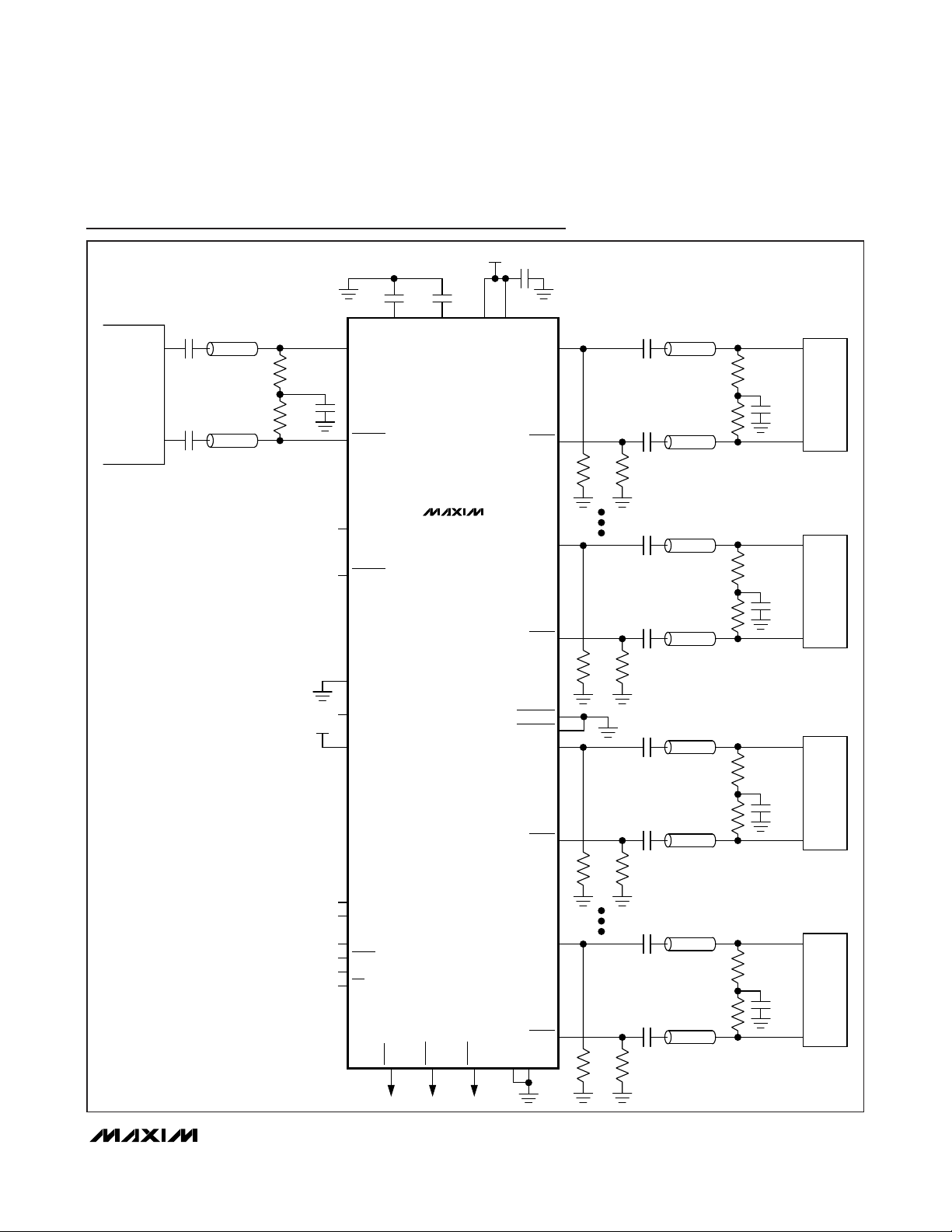
Typical Application Circuits
61.44MHz
TIMING
CARD
0.1μF
0.1μF
Z = 50Ω
Z = 50Ω
50Ω
50Ω
0.1μF
REFCLK0
REFCLK0
REFCLK1
REFCLK1
DM
CPLL
0.1μF
0.22μF
CREG
MAX3673
+3.3V
CC
V
0.1μF
OUTA3
VCC_VCO
OUTA3
OUTA0
OUTA0
150Ω
150Ω
0.1μF
0.1μF
150Ω
0.1μF
0.1μF
150Ω
Z = 50Ω
Z = 50Ω
Z = 50Ω
Z = 50Ω
153.6MHz
50Ω
50Ω
153.6MHz
50Ω
50Ω
ASIC
0.1μF
ASIC
0.1μF
+3.3V
DA
DB
SEL_CLK
PLL_BYPASS
FB_IN
FB_IN
FB_SEL
MR
LOCK
IN0FAIL
IN1FAIL
OUTA_EN
OUTB_EN
OUTB4
OUTB4
OUTB0
OUTB0
GND
EP
150Ω
150Ω
0.1μF
0.1μF
150Ω
0.1μF
0.1μF
150Ω
Z = 50Ω
Z = 50Ω
Z = 50Ω
Z = 50Ω
122.88MHz
50Ω
50Ω
122.88MHz
50Ω
50Ω
0.1μF
0.1μF
CPRI
SerDes
CPRI
SerDes
Page 16

MAX3673
Low-Jitter Frequency Synthesizer
with Selectable Input Reference
Maxim cannot assume responsibility for use of any circuitry other than circuitry entirely embodied in a Maxim product. No circuit patent licenses are
implied. Maxim reserves the right to change the circuitry and specifications without notice at any time.
16
____________________Maxim Integrated Products, 120 San Gabriel Drive, Sunnyvale, CA 94086 408-737-7600
© 2009 Maxim Integrated Products Maxim is a registered trademark of Maxim Integrated Products, Inc.
Typical Application Circuits (continued)
Chip Information
PROCESS: BiCMOS
Package Information
For the latest package outline information and land patterns, go
to www.maxim-ic.com/packages
.
PACKAGE TYPE PACKAGE CODE DOCUMENT NO.
56 TQFN-EP T5688+3
21-0135
61.44MHz
IN015.36kHz
IN115.36kHz
CLK0
MAX9450
61.44MHz
4 x 153.6MHz
5 x 122.88MHz
REFCLK0
OUTA[3:0]
MAX3673
OUTB[4:0]
 Loading...