

Page 1
General Description
The MAX3645 limiting amplifier functions as a data
quantizer and is pin compatible with the Mindspeed
MC2045-2 and MC2045-2Y postamplifiers. The amplifier accepts a wide range of input voltages and provides
constant-level positive emitter-coupled logic (PECL)
output voltages with controlled edge speeds.
The MAX3645 features an integrated power detector
with complementary PECL loss-of-signal (LOS) outputs
that indicate when the input power level drops below a
programmable threshold. An optional squelch function
holds the data outputs at static levels during a
LOS condition.
The MAX3645 operates from a single +3.3V or +5.0V
power supply over a -40°C to +85°C temperature
range. It is available in 16-pin SO and 16-pin QSOP
packages.
Applications
SONET 155Mbps Transceivers
Fast Ethernet Receivers
FDDI 125Mbps Receivers
FTTx Receivers
ESCON Receivers
Features
♦ Pin Compatible with the Mindspeed
MC2045-2/MC2045-2Y
♦ 500µV Input Sensitivity (BER = 10
-12
)
♦ Compatible with 4B/5B Data Coding
♦ Programmable LOS Threshold
♦ Stable LOS Threshold Over Supply Range
♦ Output Disable Function and Automatic Squelch
♦ Single +3.3V or +5.0V Power Supply
♦ 18mA Supply Current
MAX3645
+2.97V to +5.5V, 125Mbps to 200Mbps Limiting
Amplifier with Loss-of-Signal Detector
________________________________________________________________ Maxim Integrated Products 1
Ordering Information
19-3026; Rev 0; 10/03
For pricing, delivery, and ordering information, please contact Maxim/Dallas Direct! at
1-888-629-4642, or visit Maxim’s website at www.maxim-ic.com.
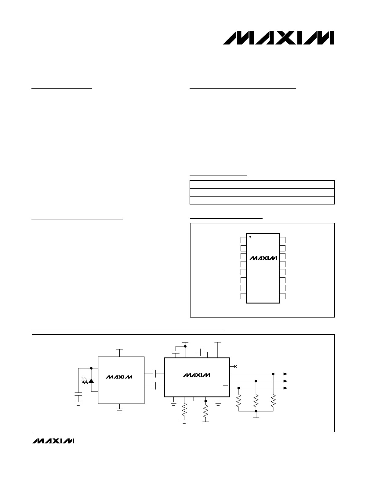
Pin Configuration
MAX3645
MAX3644*
PIN K
IN
V
CC
V
CC
V
CC
V
CC
OUT-
OUT+
DIN+
DIN-
GNDA
DOUT+
DOUT-
LOS
LOS
DIS
CSD
V
CCA CAZ1 CAZ2
GND
*FUTURE PRODUCT
V
CCE
TH GNDE
N.C.
0.1µF
0.1µF
C
SD
1nF
C
AZ
0.1µF
R
TH
100Ω
50Ω
50Ω 50Ω 50Ω
V
CC
- 2V
V
CC
- 2V
Typical Application Circuit
PART TEMP RANGE PIN-PACKAGE
MAX3645ESE -40°C to +85°C 16 SO
MAX3645EEE -40°C to +85°C 16 QSOP
TOP VIEW
CAZ2
CAZ1
GNDA
DIN+
DIN-
V
CCA
CSD
DIS
1
2
3
MAX3645
4
5
6
7
8
16
TH
15
N.C.
14
V
CCE
DOUT+
13
DOUT-
12
GNDE
11
LOS
10
LOS
9
SO/QSOP
Page 2
MAX3645
+2.97V to +5.5V, 125Mbps to 200Mbps Limiting
Amplifier with Loss-of-Signal Detector
2 _______________________________________________________________________________________
ABSOLUTE MAXIMUM RATINGS
ELECTRICAL CHARACTERISTICS
(VCC= +2.97V to +5.5V, PECL outputs are terminated with 50Ω to VCC- 2V, RTH= 100Ω, CAZ= 0.1µF, CSD= 1nF, TA= -40°C to
+85°C. Typical values are at V
CC
= +3.3V, TA = +25°C, unless otherwise noted.)
Stresses beyond those listed under “Absolute Maximum Ratings” may cause permanent damage to the device. These are stress ratings only, and functional
operation of the device at these or any other conditions beyond those indicated in the operational sections of the specifications is not implied. Exposure to
absolute maximum rating conditions for extended periods may affect device reliability.
Power-Supply Voltage (V
CCA
, V
CCE
) ....................-0.5V to +7.0V
Voltage at CAZ1, CAZ2, DIN+,
DIN-, CSD, DIS, TH ................................-0.5V to (V
CC
+ 0.5V)
PECL Output Current (DOUT+, DOUT-, LOS, LOS) ...........50mA
Differential Voltage between CAZ1 and CAZ2......-1.5V to +1.5V
Differential Voltage between DIN+ and DIN- ........-1.5V to +1.5V
Continuous Power Dissipation (T
A
= +85°C)
16-Pin SO (derate 8.7mW/°C above +85°C)................565mW
16-Pin QSOP (derate 8.3mW/°C above +85°C)...........540mW
Storage Ambient Temperature Range (T
S
)…….-65°C to +160°C
Lead Temperature (soldering, 10s)...........……………….+300°C
POWER SUPPLY
Supply Current I
INPUT SPECIFICATIONS
Input Resistance R
Input Sensitivity (Note 1) V
Input Overload (Note 1) V
Input-Referred Offset Voltage
Input Common-Mode Voltage V
Input-Referred RMS Noise V
DIS Input High V
DIS Input Low V
DIS Input Current IIL, I
OUTPUT SPECIFICATIONS
PECL Output-Voltage High (Notes 1, 2)
PECL Output-Voltage Low (Notes 1, 2)
PARAMETER SYM B O L CONDITIONS MIN TYP MAX UNITS
CC
IN-MIN
IN-MAX
CMM
IN-NOISE
Excludes PECL termination currents 18 27 mA
Single ended; VIN = ±200mV 3.3 4.8 6.4 kΩ
IN
Single ended 0.5
Differential 1.0
Single ended 750
Differential 1500
Unterminated input, output offset divided by
DC gain (Note 2)
(Notes 2, 3) 36 50 µV
PECL or CMOS logic
IH
PECL or CMOS logic 0
IL
0V ≤ V
IH
DIS
≤ V
CC
240µV
VCC -
0.87
V
-
CC
1160
-10 +10 µA
V
-
CC
1085
V
-
CC
1830
V
CC
V
CC
1480
VCC -
880
VCC 1555
-
mV
mV
P-P
P-P
V
RMS
mV
mV
mV
mV
Data Output Transition Time tR, t
Pulse-Width Distortion PWD (Notes 1, 2, 4, 5) 30 200 ps
20% to 80% (Notes 1, 2, 4) 0.7 1.4 ns
F
Page 3
MAX3645
+2.97V to +5.5V, 125Mbps to 200Mbps Limiting
Amplifier with Loss-of-Signal Detector
_______________________________________________________________________________________ 3
Note 1: Between sensitivity and overload, the output amplitude is >95% of the fully limited amplitude and all AC specifications are met.
Note 2: Guaranteed by design and characterization.
Note 3: Noise is derived from BER measurement.
Note 4: The data input transition time is controlled by a 4th-order Bessel filter with f
-3dB
= 0.75 × data rate.
Note 5: PWD = [(width of wider pulse) - (width of narrower pulse)] / 2, measured with 155Mbps 0011 pattern.
Note 6: All LOS specifications are measured using a 155Mbps 2
23
- 1 PRBS pattern.
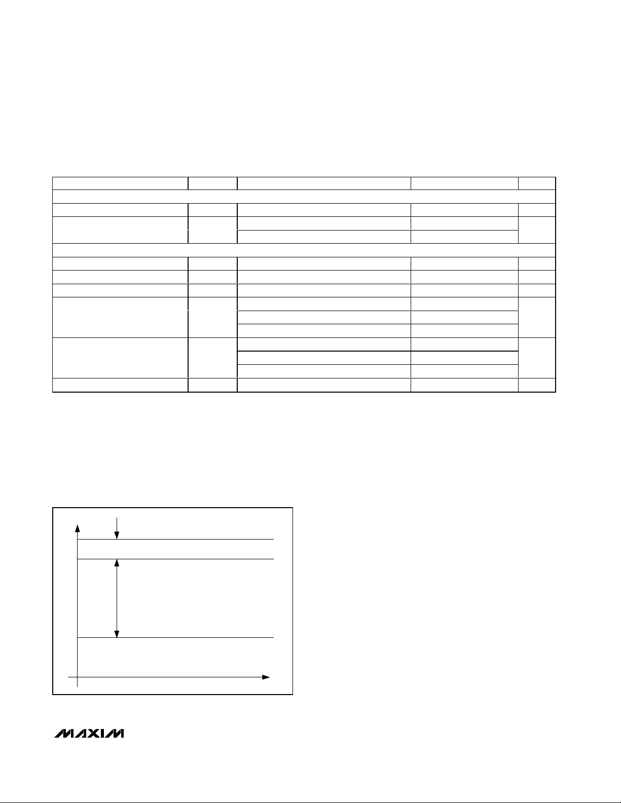
Note 7: The signal at the input is switched between two amplitudes, SIGNAL_ON and SIGNAL_OFF, as shown in Figure 1.
ELECTRICAL CHARACTERISTICS (continued)
(VCC= +2.97V to +5.5V, PECL outputs are terminated with 50Ω to VCC- 2V, RTH= 100Ω, CAZ= 0.1µF, CSD= 1nF, TA= -40°C to
+85°C. Typical values are at V
CC
= +3.3V, TA = +25°C, unless otherwise noted.)
Figure 1. Signal Levels for LOS Assert/Deassert Time
Measurement
TRANSFER CHARACTERISTICS
Bandwidth Gain = 60dB 150 250 MHz
Low-Frequency Cutoff
LOSS-OF-SIGNAL SPECIFICATIONS (Notes 2, 4, 6)
LOS Sensitivity Range 0Ω ≤ RTH ≤ 2kΩ 220mV
LOS Hysteresis 10log (V
LOS Assert/Deassert Time (Note 7) 2.3 80.0 µs
Signal-Dectect Filter Resistance R
PARAMETER SYM B O L CONDITIONS MIN TYP MAX UNITS
CAZ = open 500
= 0.1µF 0.5
C
AZ
DEASSERT/VASSERT
RTH = 0Ω, low setting 0.5 0.9 1.3
RTH = 1kΩ, medium setting 4.8 6.6 8.3LOS Assert Level
= 2kΩ, high setting 12 17 22
R
TH
RTH = 0Ω, low setting 1.1 1.5 1.9
RTH = 1kΩ, medium setting 8.0 10.8 13.5LOS Deassert Level
= 2kΩ, high setting 20 28 36
R
TH
Pin 7 14 20 26 kΩ
SD
kHz
) 1.4 2 dB
mV
mV
P-P
P-P
P-P
V
IN
SIGNAL ON
1dB
6dB MAXIMUM POWER-DETECT WINDOW
0V
MAXIMUM DEASSERT LEVEL
MINIMUM ASSERT LEVEL
SIGNAL OFF
TIME
Page 4

MAX3645
+2.97V to +5.5V, 125Mbps to 200Mbps Limiting
Amplifier with Loss-of-Signal Detector
4 _______________________________________________________________________________________
Typical Operating Characteristics
(VCC= 3.3V, PECL outputs terminated with 50Ω to VCC- 2V, RTH= 100Ω, CAZ= 0.1µF, CSD= 1nF, TA= +25°C, unless otherwise noted.)
SUPPLY CURRENT vs. TEMPERATURE
(EXCLUDES PECL OUTPUT CURRENTS)
MAX3645 toc01
TEMPERATURE (°C)
SUPPLY CURRENT (mA)
603510-15
10
15
20
25
30
35
40
45
50
5
-40 85
VCC = 5.0V
VCC = 3.3V
OUTPUT EYE DIAGRAM
(V
IN
= 1mV
P-P
, 155Mbps, 223 - 1PRBS)
MAX3654 toc02
1ns/div
200mV/
div
OUTPUT EYE DIAGRAM
(V
IN
= 1500mV
P-P
, 155Mbps, 223 - 1PRBS)
MAX3645 toc03
1ns/div
200mV/
div
TRANSFER FUNCTION
MAX3654 toc04
DIFFERENTIAL INPUT VOLTAGE (mV
P-P
)
DIFFERENTIAL OUTPUT VOLTAGE (mV
P-P
)
1010.1
600
800
1000
1200
1400
1600
1800
2000
400
0.01 100
RTH = 1kΩ
RTH = 2kΩ
RTH = 100Ω
RTH = 0Ω
BIT-ERROR RATIO vs.
DIFFERENTIAL INPUT VOLTAGE
MAX3645 toc05
DIFFERENTIAL INPUT VOLTAGE (mV
P-P
)
BIT-ERROR RATIO
0.70.60.4 0.50.2 0.30.1
10
-3
10
-4
10
-5
10
-6
10
-7
10
-8
10
-9
10
-10
10
-11
10
-12
0 0.8
155Mbps, 223 - 1 PRBS
INPUT-REFERRED RMS NOISE
vs. TEMPERATURE
MAX3645 toc06
TEMPERATURE (°C)
INPUT-REFERRED NOISE (µV
RMS
)
603510-15
20
25
30
35
40
45
50
55
60
65
70
75
80
85
15
-40 85
VCC = +5.0V
VCC = +3.3V
SMALL-SIGNAL GAIN vs. R
TH
MAX3645 toc07
RTH (kΩ)
20log (V
OUT
/V
IN
) (dB)
1.71.51.0 1.20.5 0.70.2
10
20
30
40
50
60
70
80
90
100
0
0 2.0
VIN = 0.1mV
P-P
LOSS-OF-SIGNAL THRESHOLD
vs. R
TH
(VCC = +3.3V AND +5.0V)
MAX3645 toc08
RTH (kΩ)
DIFFERENTIAL INPUT VOLTAGE (mV
P-P
)
1.81.61.2 1.40.4 0.6 0.8 1.00.2
2
4
6
8
10
12
14
16
18
20
22
24
26
28
30
0
0 2.0
LOS DEASSERT
LOS ASSERT
155Mbps, 223 - 1 PRBS
LOSS-OF-SIGNAL HYSTERESIS
vs. TEMPERATURE
MAX3645 toc09
TEMPERATURE (°C)
10log (DEASSERT/ASSERT) (dB)
603510-15
1.4
1.6
1.8
2.0
2.2
2.4
2.6
2.8
3.0
3.2
1.2
-40 85
RTH = 2kΩ
RTH = 100Ω
RTH = 1kΩ
155Mbps, 223 - 1 PRBS
Page 5

MAX3645
+2.97V to +5.5V, 125Mbps to 200Mbps Limiting
Amplifier with Loss-of-Signal Detector
_______________________________________________________________________________________ 5
Typical Operating Characteristics (continued)
(VCC= 3.3V, PECL outputs terminated with 50Ω to VCC- 2V, RTH= 100Ω, CAZ= 0.1µF, CSD= 1nF, TA= +25°C, unless otherwise noted.)
LOSS-OF-SIGNAL WITH SQUELCH
(155Mbps, 2
23
- 1PRBS)
MAX3654 toc10
10µs/div
LOS
V
OUT
V
IN
PULSE-WIDTH DISTORTION
vs. DIFFERENTIAL INPUT VOLTAGE
MAX3645 toc11
DIFFERENTIAL INPUT VOLTAGE (mV
P-P
)
PULSE-WIDTH DISTORTION (ps)
1000100101
10
20
30
40
50
60
70
80
90
100
0
0.1 10,000
155Mbps 0011 PATTERN
DATA OUTPUT TRANSITION TIME
vs. DIFFERENTIAL INPUT VOLTAGE
MAX3645 toc12
DIFFERENTIAL INPUT VOLTAGE (mV
P-P
)
TRANSITION TIME (ns)
1000100101
0.5
1.0
1.5
2.0
2.5
3.0
0
0.1 10,000
Page 6

MAX3645
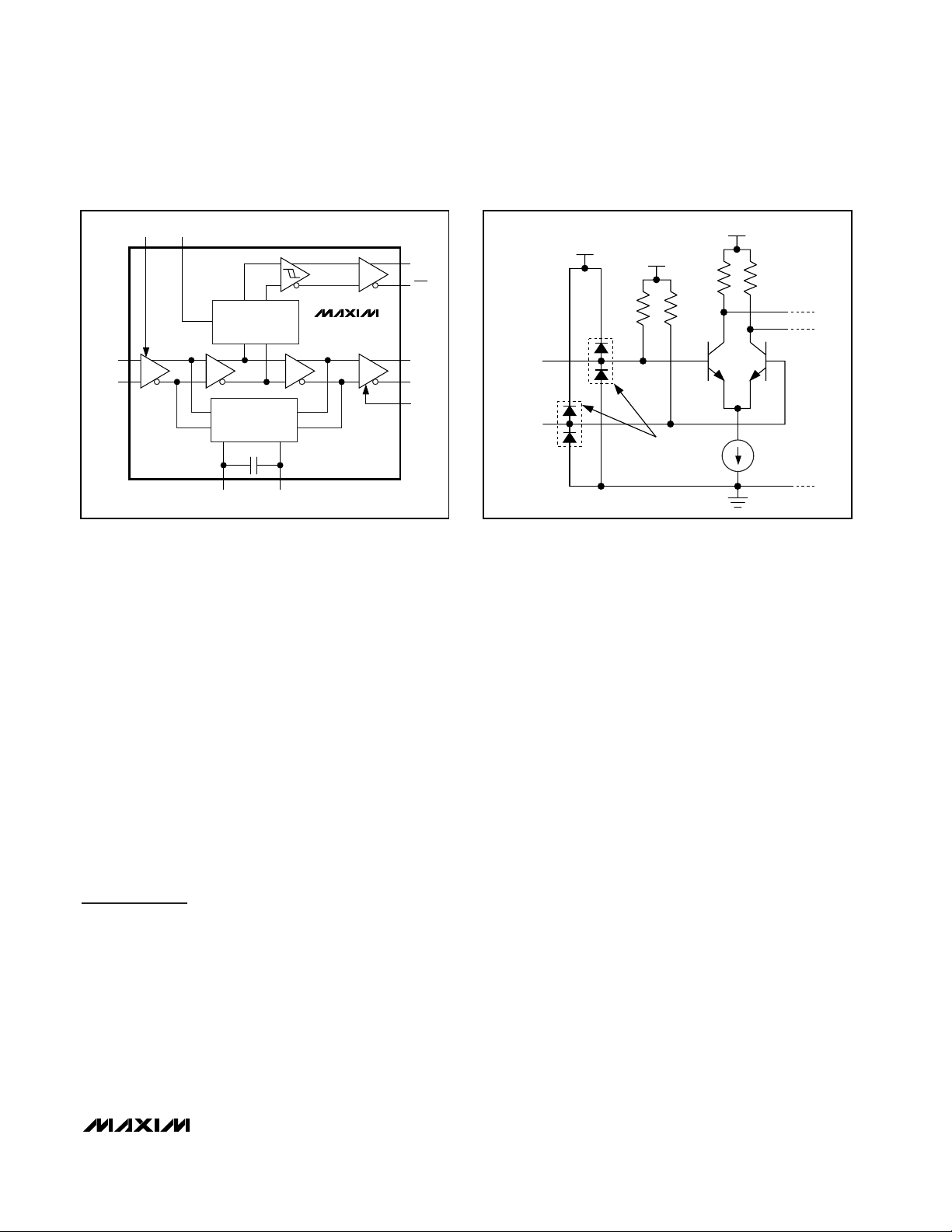
Detailed Description
The MAX3645 consists of gain stages, offset correction,
power detector, LOS indicators, and PECL output buffers.
See Figure 2 for the functional diagram.
Data Input
The data inputs have a single-ended input resistance of
4.8kΩ and are internally DC-biased to V
CC
- 0.87V (see
Figure 3). External capacitors are required to AC-couple the data signals. Pattern-dependent jitter is minimized by using coupling capacitor values large enough
to pass the lowest frequencies of interest (consecutive
ones and zeros) with the given input resistance.
Typically, 0.1µF coupling capacitors yield a -3dB frequency of 354Hz. Capacitor tolerance and input resis-
tance variation (3.3kΩ to 6.4kΩ) must be considered to
accurately calculate the -3dB frequency. Capacitor values should be chosen that set the -3dB frequency at
least a factor of 10 below the lowest frequency of interest. A capacitor value of 0.1µF is recommended.
Gain Stage and Offset Correction
The limiting amplifier provides approximately 74dB
(RTH= 100Ω) of gain. This large gain makes the amplifier susceptible to small DC offsets in the signal path.
To correct DC offsets, the amplifier has an internal feedback loop that acts as a DC autozero circuit. By correcting the DC offsets, the limiting amplifier improves
receiver sensitivity and power-detector accuracy.
+2.97V to +5.5V, 125Mbps to 200Mbps Limiting
Amplifier with Loss-of-Signal Detector
6 _______________________________________________________________________________________
Pin Description
MINDSPEED
MC2045-2
PIN
MC2045-2Y
PIN NAME
1 CAZ- CAZ2
2 CAZ+ CAZ1
3 GNDA GNDA Analog Supply Ground. Must be at the same potential as the GNDE pin.
4DINDIN+ Positive Data Input
5DINDIN- Negative Data Input
6V
7CFCSD S i g nal - D etect- Fi l ter C ap aci tor C onnecti on. C onnect the C
8 JAM DIS
9 ST LOS
10 ST LOS
11 GNDE GNDE Digital Supply Ground. Must be at the same potential as the GNDA pin.
12 D
13 D
14 V
15 NC N.C. No Connection
16 V
CCA
OUT
OUT
CCE
SET
MAXIM
MAX3645
PIN NAME
Offset-Correction-Loop Capacitor Connection. A capacitor connected between this pin and
CAZ1 sets the time constant of the offset correction loop. The offset correction is disabled
when the CAZ1 and CAZ2 pins are shorted together.
Offset-Correction-Loop Capacitor Connection. A capacitor connected between this pin and
CAZ2 sets the time constant of the offset correction loop. The offset correction is disabled
when the CAZ2 and CAZ1 pins are shorted together.
V
CCA
DOUT- Negative Data Output, PECL. A high at DIS forces DOUT- high.
DOUT+ Positive Data Output, PECL. A high at DIS forces DOUT+ low.
V
CCE
TH
+2.97V to +5.5V Analog Supply Voltage. Must be at same potential as the V
Disable Input, PECL or CMOS Compatible. Data outputs are held to a static logic 0 when DIS is
asserted high. The LOS function remains active when the outputs are disabled. When
connected to the LOS pin, an automatic squelch function is enabled.
Positive Loss-of-Signal Output, PECL. LOS is high when the level of the input signal drops
below the threshold set by the TH input. LOS is low when the signal level is above the
threshold. LOS can be connected directly to DIS for automatic squelch.
Negative Loss-of-Signal Output, PECL. LOS is low when the level of the input signal drops
below the threshold set by the TH input. LOS is high when the signal level is above the
threshold.
+2.97V to +5.5V Digital Supply Voltage. Must be at the same potential as the V
Loss-of-Signal Threshold Pin. Resistor (R
be left open.
FUNCTION
) to ground sets the LOS threshold. This pin cannot
TH
pin.
CCE
cap aci tor b etw een C S D and V
S D
CCA
pin.
C C A
.
Page 7
The external autozero capacitor (CAZ), in parallel with
internal capacitance (C
INT
), determines the time constant of the DC offset correction loop. With CAZ= 0.1µF
(recommended), the -3dB frequency cutoff of the signal
path is typically 0.5kHz.
Power Detector and LOS Indicators
The external resistor RTHsets the gain of the first limiting stage. This gain setting controls the threshold at
which the power detector indicates an LOS condition.
Power detection is accomplished by rectifying and lowpass filtering the data signal, then comparing it to the
programmed threshold voltage. A hysteresis of 2dB
prevents the LOS output from chattering when the input
signal is near the threshold.
PECL Output Buffer
The data outputs (DOUT+, DOUT-) and the loss-of-signal outputs (LOS+, LOS-) are PECL outputs. The equivalent PECL output circuit is shown in Figure 4.
Applications Information
Programming LOS Assert/Deassert Levels
The appropriate value of RTHis determined by using
the Loss-Of-Signal Threshold vs. RTHgraph in the
Typical Operating Characteristics.
LOS Time Constant
The lowpass filter of the power detector comprises a
20kΩ on-chip resistor (RSD) and an external capacitor
(CSD). The CSDcapacitor value determines the power-
detector time constant, which determines the LOS
assert/deassert time. With C
SD
= 1nF the assert/
deassert time is in the range of 2.3µs to 80µs. This provides a long enough time constant to avoid false triggering due to variations in mark density.
Disable Function
When the DIS input is forced high, the disable function
is enabled, which holds DOUT+ low and DOUT- high.
The disable function is used to prevent the data outputs
from toggling due to noise when no signal is present.
The LOS output can be connected to the DIS input for
automatic squelch.
PECL Output Terminations
The proper termination for a PECL output is 50Ω to
(VCC- 2V), but other standard termination techniques
can be used. For more information on PECL terminations and how to interface with other logic families, refer
to Maxim Application Note HFAN-01.0: Introduction to
LVDS, PECL, and CML.
Layout Considerations
For best performance, use good high-frequency layout
techniques. Filter power supplies, keep ground connections short, and use multiple vias where possible.
Power-supply decoupling should be placed close to
the V
CC
pins. Minimize the distance from the preamplifier and use controlled-impedance transmission lines to
interface with the outputs when possible.
MAX3645
+2.97V to +5.5V, 125Mbps to 200Mbps Limiting
Amplifier with Loss-of-Signal Detector
_______________________________________________________________________________________ 7
Figure 2. Functional Diagram
Figure 3. Equivalent Data Input Circuit
CSD
TH
LOS
LOS
POWER
DETECTOR
DIN+
DIN-
CORRECTION
CAZ1 CAZ2
OFFSET
C
INT
MAX3645
DOUT+
DOUT-
DIS
V
CC
V
CC
DIN+
DIN-
- 0.87V
V
CC
4.8kΩ 4.8kΩ
ESD
STRUCTURES
Page 8

MAX3645
+2.97V to +5.5V, 125Mbps to 200Mbps Limiting
Amplifier with Loss-of-Signal Detector
8 _______________________________________________________________________________________
Figure 4. Equivalent PECL Output Circuit
Chip Information
TRANSISTOR COUNT: 1026
PROCESS: Silicon bipolar
V
CC
DOUT+/LOS
DOUT+/LOS
ESD
STRUCTURES
Page 9

MAX3645
+2.97V to +5.5V, 125Mbps to 200Mbps Limiting
Amplifier with Loss-of-Signal Detector
_______________________________________________________________________________________ 9
Package Information
(The package drawing(s) in this data sheet may not reflect the most current specifications. For the latest package outline information,
go to www.maxim-ic.com/packages
.)
N
1
TOP VIEW
D
e
FRONT VIEW
INCHES
DIM
MIN
0.053A
0.004
A1
0.014
B
0.007
C
e 0.050 BSC 1.27 BSC
0.150
HE
A
B
A1
C
L
E
H 0.2440.228 5.80 6.20
0.016L
VARIATIONS:
INCHES
MINDIM
D
0.189 0.197 AA5.004.80 8
0.337 0.344 AB8.758.55 14
D
0-8
SIDE VIEW
MAX
0.069
0.010
0.019
0.010
0.157
0.050
MAX
0.3940.386D
MILLIMETERS
MAX
MIN
1.35
1.75
0.10
0.25
0.35
0.49
0.19
0.25
3.80 4.00
0.40 1.27
MILLIMETERS
MAX
MIN
9.80 10.00
N MS012
16
AC
SOICN .EPS
PROPRIETARY INFORMATION
TITLE:
PACKAGE OUTLINE, .150" SOIC
REV.DOCUMENT CONTROL NO.APPROVAL
21-0041
1
B
1
Page 10

MAX3645
+2.97V to +5.5V, 125Mbps to 200Mbps Limiting
Amplifier with Loss-of-Signal Detector
Maxim cannot assume responsibility for use of any circuitry other than circuitry entirely embodied in a Maxim product. No circuit patent licenses are
implied. Maxim reserves the right to change the circuitry and specifications without notice at any time.
10 ____________________Maxim Integrated Products, 120 San Gabriel Drive, Sunnyvale, CA 94086 408-737-7600
© 2003 Maxim Integrated Products Printed USA is a registered trademark of Maxim Integrated Products.
Package Information (continued)
(The package drawing(s) in this data sheet may not reflect the most current specifications. For the latest package outline information,
go to www.maxim-ic.com/packages
.)
QSOP.EPS
PACKAGE OUTLINE, QSOP .150", .025" LEAD PITCH
1
21-0055
E
1
 Loading...