

Page 1
General Description
The MAX3634 burst-mode clock phase aligner (CPA) is
designed specifically for 622Mbps or 1244Mbps GPON
(ITU G.984) optical line terminal (OLT) receiver applications. The MAX3634 provides clock and clock-aligned
resynchronized upstream data through differential
LVPECL outputs. Using the OLT system clock as a reference, the MAX3634 aligns to the input data and
acquires within the first 13 bits of the burst. The CPA
operates with received data that is frequency locked to
the OLT reference. The acquisition time, bit-error ratio,
and jitter tolerance all support GPON PMD specifications. LVPECL high-speed clock and data outputs provide compatibility with FPGAs at 622Mbps and with the
MAX3885 deserializer at 1244Mbps.
The MAX3634 is available in a low-profile, 7mm x 7mm,
48-lead TQFN package. The MAX3634 operates from a
single +3.3V supply, over the -40°C to +85°C temperature range.
Applications
622Mbps GPON OLT Receivers
1244Mbps GPON OLT Receivers
Features
♦ DC-Coupled Clock Phase Aligner for Burst-Mode
GPON Applications
♦ 13-Bit Burst Acquisition Time
♦ 0.85UI High-Frequency Jitter Tolerance
♦ Continuous Clock Output
♦ Byte Rate (1/8th Data Rate) Reference Clock Input
♦ Lock Detect Output
♦ LVPECL Serial Data Input and Output
♦ LVPECL Reset Input
MAX3634
622Mbps/1244Mbps Burst-Mode Clock Phase
Aligner for GPON OLT Applications
________________________________________________________________ Maxim Integrated Products 1
Ordering Information
19-3818; Rev 0; 9/05
For pricing, delivery, and ordering information, please contact Maxim/Dallas Direct! at
1-888-629-4642, or visit Maxim’s website at www.maxim-ic.com.
Typical Application Circuit
Pin Configuration appears at end of data sheet.
PART TEMP RANGE
MAX3634ETM -40°C to +85°C
PINPACKAGE
48 TQFN
(7mm x 7mm)
PKG
CODE
T4877-6
BURST RESET
DATA
CLOCK
OLT CLOCK
DATA
BURST ENABLE
4
DATA
MAX3634
BURST-MODE
CLOCK PHASE
ALIGNER
DIVIDE BY 8
RATESEL
GPON OPTICAL LINE TERMINATION GPON OPTICAL NETWORK TERMINATION
BURST-MODE
TIA/LA
MAX3738
CONTINUOUS
LASER DRIVER
UPSTREAM
1244Mbps
DOWNSTREAM
2488Mbps
MAX3656
BURST-MODE
LASER DRIVER
MAX3864
MAX3748A
TIA/LA
MAX3892
DATA
SERIALIZER
MAX3872
SONET
CDR
CLOCK
DIVIDE BY 16
CLOCK
DATA
Page 2
MAX3634
622Mbps/1244Mbps Burst-Mode Clock Phase
Aligner for GPON OLT Applications
2 _______________________________________________________________________________________
ABSOLUTE MAXIMUM RATINGS
ELECTRICAL CHARACTERISTICS
(VCC= +3.0V to +3.6V, TA= -40°C to +85°C. Typical values are at VCC= +3.3V, TA= +25°C, unless otherwise noted.)
Stresses beyond those listed under “Absolute Maximum Ratings” may cause permanent damage to the device. These are stress ratings only, and functional
operation of the device at these or any other conditions beyond those indicated in the operational sections of the specifications is not implied. Exposure to
absolute maximum rating conditions for extended periods may affect device reliability.
VCC, VCCI, VCCO, VCCV ........................................-0.5V to +4.0V
SDI±, RST±, REFCLK±,
RATESEL, FILT, TEST.............................-0.5V to (V
CC
+ 0.5V)
LVPECL Output Current (SDO±, SCLK±, LOCK±).............50mA
Continuous Power Dissipation (T
A
= +85°C)
48-Lead TQFN package
(derate 27.8mW/°C above +85°C).............................1800mW
Storage Temperature Range .............................-55°C to +150°C
Operating Ambient Temperature Range .............-40°C to +85°C
Lead Temperature (soldering, 10s) .................................+400°C
PARAMETER SYMBOL CONDITIONS MIN TYP MAX UNITS
Supply Current I
Data Rate
Reference Clock Input Frequency
SDI, RST, REFCLK Differential
Input
SDI±, RST±, REFCLK± Input
Current
RST Input Rise/Fall Times tr, t
SDI±, RST±, REFCLK± CommonMode Input
SDO±, SCLK±, LOCK± Output
Voltage Low
SDO±, SCLK±, LOCK± Output
Voltage High
Jitter Tolerance
Acquisition Time (Notes 2, 3) 13 Bits
Bit-Error Ratio After acquisition (Notes 2, 4) 10
SDO±, LOCK± Transition Time tr, t
SCLK± Transition Time tr, t
CC
V
V
V
OH
Not including LVPECL output current 315 390 mA
RATESEL = low 1244.16
RATESEL = high 622.08
RATESEL = low 155.52
RATESEL = high 77.76
IN
Rate = 1244Mbps 200
f
Rate = 622Mbps 200
- 1.49
TA = 0°C to +85°C (Note 1)
OL
TA = -40°C to 0°C (Note 1)
TA = 0°C to +85°C (Note 1)
TA = -40°C to 0°C (Note 1)
622Mbps (Notes 2, 5, 6) 0.73 0.83
1244Mbps (Notes 2, 5, 6) 0.73 0.81
20% to 80% (Note 1) 265 ps
f
20% to 80% (Note 1) 200 ps
f
- 1.81
- 1.83
- 1.025
- 1.085
200 1600 mV
-180 +180 µA
V
CC
V
CC
V
CC
V
CC
V
CC
V
CC
- VIN/4
V
CC
- 1.62
V
CC
- 1.555
V
CC
- 0.88
V
CC
- 0.88
-10
Mbps
MHz
P-P
ps
V
V
V
UI
P-P
Page 3
MAX3634
622Mbps/1244Mbps Burst-Mode Clock Phase
Aligner for GPON OLT Applications
_______________________________________________________________________________________ 3
ELECTRICAL CHARACTERISTICS (continued)
(VCC= +3.0V to +3.6V, TA= -40°C to +85°C. Typical values are at VCC= +3.3V, TA= +25°C, unless otherwise noted.)
Note 1: PECL output must have external termination of 50Ω to VCC- 2V (Thevenin equivalent).
Note 2: AC parameters are guaranteed by design and characterization.
Note 3: From start of PON burst, 101010101010 preamble sequence.
Note 4: BER, acquisition time requirements are met with 100mV
P-P
sinusoidal noise on VCC, 0 < f
NOISE
≤ 10MHz.
Note 5: Measured with 20ps
RMS
input random jitter (1.244Mbps), 30ps
RMS
(622Mbps)
Note 6: Jitter tolerance refers to the variation in phase between REFCLK and SDI after acquisition.
Typical Operating Characteristics
(VCC= +3.3V and TA= +25°C, unless otherwise noted)
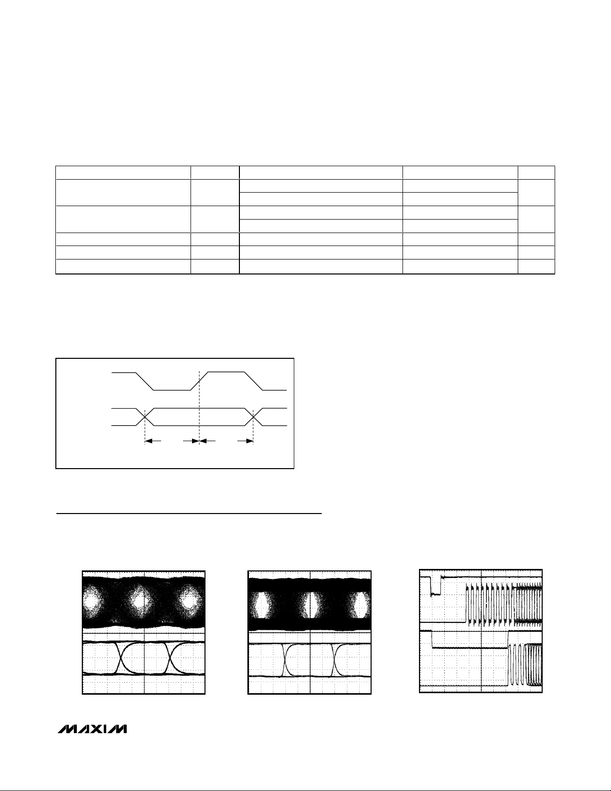
1.244Gbps
INPUT AND OUTPUT EYE DIAGRAMS
MAX3634 toc01
200ps/div
SDI
SDO
622Mbps
INPUT AND OUTPUT EYE DIAGRAMS
MAX3634 toc02
400ps/div
SDI
SDO
BURST CAPTURE AT 1.244Gbps
MAX3634 toc03
1ns/div
RST
SDI
SDO
LOCK
Figure 1. Definition of Clock-to-Q and Q-to-Clock Delay
PARAMETER SYMBOL CONDITIONS MIN TYP MAX UNITS
Serial Data Output Clock-to-Q
Delay (Figure 1)
Serial Data Output Q-to-Clock
Delay (Figure 1)
t
CLK-Q
t
Q-CLK
RATESEL Input High V
RATESEL Input Low V
RATESEL Input Current VIN = 0V or V
(SCLK+) - (SCLK-)
(SDO+) - (SDO-)
622Mbps (Notes 1, 2) 500
1244Mbps (Notes 1, 2) 250
622Mbps (Notes 1, 2) 500
1244Mbps (Notes 1, 2) 250
IH
IL
CC
2V
-100 +100 µA
ps
ps
0.8 V
t
CLK-Q
t
Q-CLK
Page 4

MAX3634
622Mbps/1244Mbps Burst-Mode Clock Phase
Aligner for GPON OLT Applications
4 _______________________________________________________________________________________
Pin Description
Typical Operating Characteristics (continued)
(VCC= +3.3V and TA= +25°C, unless otherwise noted)
JITTER TOLERANCE vs. SDI-TO-REFCLK
PHASE (1.244Gbps)
MAX3634 toc04
SDI-TO-REFCLK PHASE (ps)
JITTER TOLERANCE (UI
P-P
)
600400200
0.1
0.2
0.3
0.4
0.5
0.6
0.7
0.8
0.9
1.0
0
0 800
LIMITED BY TEST EQUIPMENT
JITTER TOLERANCE vs. SDI-TO-REFCLK
PHASE (622Mbps)
MAX3634 toc05
SDI-TO-REFCLK PHASE (ps)
JITTER TOLERANCE (UI
P-P
)
600400200
0.1
0.2
0.3
0.4
0.5
0.6
0.7
0.8
0.9
1.0
0
0 800
LIMITED BY TEST EQUIPMENT
SUPPLY CURRENT
vs. TEMPERATURE
MAX3634 toc06
AMBIENT TEMPERATURE (°C)
SUPPLY CURRENT (mA)
500
220
240
260
280
300
320
340
200
-50 100
EXCLUDES PECL OUTPUT CURRENT
PIN NAME FUNCTION
1, 2, 12, 25, 36, 37, 48 GND Supply Ground
3, 6, 7, 10 VCCI +3.3V Supply for Input Buffers
4 SDI+ Positive Serial Data Input, LVPECL
5 SDI- Negative Serial Data Input, LVPECL
8 RST+ Positive Reset Input, LVPECL. Reset (= RST+ - RST-) is falling edge triggered.
9 RST- Negative Reset Input, LVPECL
11, 38, 39, 44, 47 V
13–20, 22, 23 TEST Production Test Pins, Reserved. Leave open for normal operation.
21, 24, 26, 29, 32, 35 VCCO +3.3V Supply for Output Buffers
27 LOCK- Negative Lock Status Output, LVPECL
28 LOCK+
30 SDO- Negative Serial Data Output, LVPECL
31 SDO+ Positive Serial Data Output, LVPECL
33 SCLK- Negative Serial Clock Output, LVPECL
34 SCLK+ Positive Serial Clock Output, LVPECL
40 RATESEL Rate Select Input, TTL. High selects 622.08Mbps operation.
41, 43 VCCV +3.3V Supply for VCO
42 FILT PLL Filter Capacitor. Connect a 0.1µF X7R capacitor from pin 42 to VCCV.
45 REFCLK- Negative Reference Clock Input, LVPECL (1/8th data rate)
46 REFCLK+ Positive Reference Clock Input, LVPECL
EP Exposed Pad The exposed pad must be connected to the ground plane for proper thermal performance.
CC
+3.3V Supply for Digital Circuitry
Positive Lock Status Output, LVPECL. Lock (= (LOCK+) - (LOCK-)) high indicates that the
MAX3634 has acquired the correct phase.
Page 5

General Description
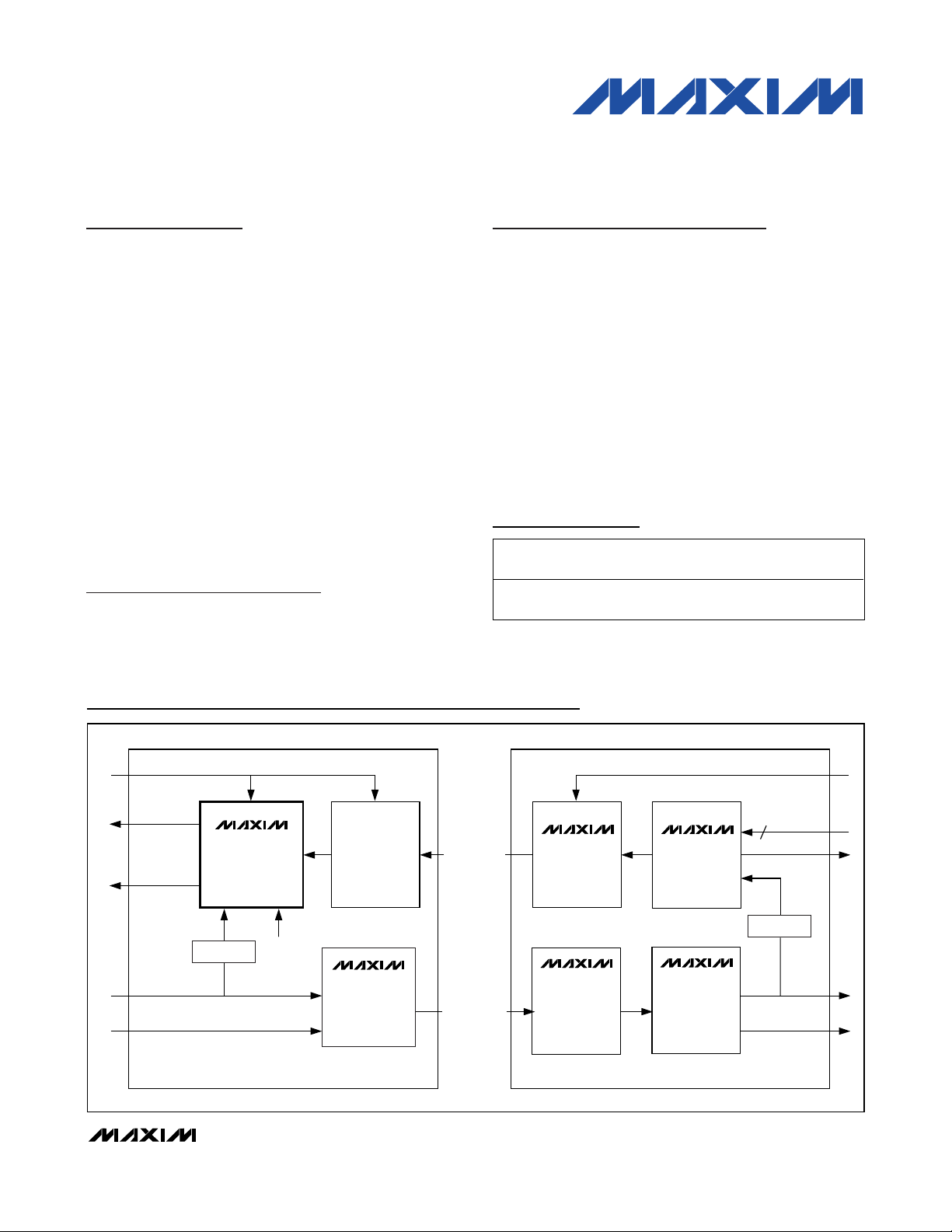
Theory of Operation
The MAX3634 CPA provides serial clock and data outputs for GPON upstream bursts.
The burst-mode CPA operates on the principle that the
recovered clock from the ONT CDR is used at each
ONT to clock upstream data bursts out of the ONT controller. The burst-mode CPA has logic that determines
the correct phase relationship between the upstream
data and the OLT reference clock at the beginning of
each ONT’s burst, and resamples the upstream data at
each bit using that clock.
The burst-mode CPA contains a phase-locked loop
(PLL) that synchronizes its oscillator to the reference
clock input. This oscillator drives a phase splitter, which
generates eight evenly spaced phases of the serial
clock, which are used to sample the input data at 1/8th
bit intervals in eight flip-flops. Combinatorial and
sequential logic measures the preamble, and based on
the phase of the preamble, determines which one of
the eight clock phases is at the center of the input data
bits. The data from the flip-flop associated with this
phase is then steered through a multiplexer to the CPA
output, which requires four or five additional clock periods until valid data is output. The CPA serial output
clock is continuous, without any phase jumps or discontinuities from burst to burst.
The burst-mode CPA requires a preamble sequence of
1010101010101 (13 bits) for correct phase alignment.
Typically, output begins after the 12th bit, although for
certain data/phase relationships, 13 bits are required.
An LVPECL-compatible lock status output is provided,
which indicates when the correct phase has been
acquired and valid serial output data is available. This
output remains low until reset by the burst reset input
(RST). The output data is disabled (held low) during the
period between reset and lock.
Reference Clock Input
The MAX3634 includes a PLL, which multiplies the reference clock by eight for use in the retiming circuitry.
For correct operation, the REFCLK input must be connected to the OLT byte-rate reference clock, which
must be equal to 1/8th the serial data rate, and must
have a 40% to 60% duty cycle. This must be the same
clock source used to time the downstream data, and
the upstream data must be frequency locked to this
source.
The RATESEL input is used to configure 622Mbps or
1244Mbps operation; when RATESEL is high, the
MAX3634 operates at 622Mbps.
MAX3634
622Mbps/1244Mbps Burst-Mode Clock Phase
Aligner for GPON OLT Applications
_______________________________________________________________________________________ 5
Figure 2. Functional Block Diagram
REFCLK+
REFCLK-
RATESEL
LVPECL
TTL
SDI+
LVPECL
SDI-
RST+
LVPECL
RST-
622Mbps/1244Mbps
PLL/PHASE SPLITTER
0
φ
7
φ
PHASE-ACQUISITION LOGIC
DQ
DQ
DQ
MUX
MAX3634
BURST-MODE CPA
SYNCHRONIZER
LVPECL
LVPECL
LVPECL
SDO+
SDO-
SCLK+
SCLK-
LOCK+
LOCK-
Page 6

MAX3634
Input Stage
The LVPECL serial data input, SDI±, and burst-mode
reset input, RST±, provide 200mV
P-P
sensitivity. The
RST± input rise and fall times (20% to 80%) must not
exceed 200ps. LVPECL inputs must be DC-coupled with
external termination for correct operation with burst data
(see Maxim Application Note HFAN 1.0 for termination
configuration).
Lock Detect
After the first 12 or 13 bits of the preamble, plus 4 or 5
bits of synchronizer delay, LOCK asserts to indicate the
beginning of valid data output.
Applications Information
GPON Burst-Mode Timing
Internally, the MAX3634 requires five internal clock
cycles (8x REFCLK) to initialize itself after receiving the
rest (BRST) signal. It then uses the next 8 bits of preamble (10101010) to measure the phase relationship
between the reference clock and upstream data (after
the internal logic has been reset), and 3 to 5 bits later
begins outputting data. The time interval from BRST to
the end of the preamble must be no less than 18 bits
long. If the 8 bits of preamble that it uses to measure
phase have been excessive pulse-width distortion, the
phase measurement is in error.
The active edge of the reset input (BRST) must arrive at
the MAX3634 after the TIA has finished its level recovery,
but no sooner than 18 bits prior to the end of the (repeating 10 pattern) preamble, in order to provide adequate
time for the MAX3634 to initialize, measure the phase,
and load the output pipelines. This timing is shown in
Figure 3.
622Mbps/1244Mbps Burst-Mode Clock Phase
Aligner for GPON OLT Applications
6 _______________________________________________________________________________________
Figure 3. Clock Phase Aligner Operation Timing Diagram
DATA INPUT
TO MAX3634
T
DSR
RESET
T
: BURST-TO-BURST SEPARATION TIME
DSR
: TIA/LA LEVEL RECOVERY TIME
T
LR
: CPA RESET AND ACQUISITION TIME, ≥ 19 BITS
T
CR
DATA VALID GUARD TIME TIA/LA ACQUISITION CPA RESET
T
LR
(5 BITS)
T
CR
CPA ACQUISITION
(12 OR 13 BITS)
OUTPUT DATA
VALID
Page 7

MAX3634
622Mbps/1244Mbps Burst-Mode Clock Phase
Aligner for GPON OLT Applications
_______________________________________________________________________________________ 7
Pin Configuration Chip Information
TRANSISTOR COUNT: 10,805
PROCESS: Silicon Germanium BiCMOS
O
CC
GND
V
36
35 34 33 32 31 30 29 28 27 26 25
GND
37
V
38
CC
V
39
CC
RATESEL
40
V
V
41
CC
FILT
42
V
V
43
CC
V
44
CC
REFCLK-
45
REFCLK+
46
V
47
CC
GND
48
*EP MUST BE CONNECTED TO GROUND.
EP*
123456789101112
GND
GND
SCLK+
I
CC
V
SCLK-
SDI+
O
CC
V
MAX3634
SDI-
TQFN
SDO+
I
CC
V
SDO-
I
CC
V
O
CC
V
RST+
LOCK+
RST-
LOCK-
I
CC
V
O
CC
V
GND
24
O
V
CC
23
TEST10
22
TEST9
21
O
V
CC
20
TEST8
19
TEST7
TEST6
18
TEST5
17
TEST4
16
TEST3
15
TEST2
14
TEST1
13
CC
V
GND
Page 8

MAX3634
622Mbps/1244Mbps Burst-Mode Clock Phase
Aligner for GPON OLT Applications
Maxim cannot assume responsibility for use of any circuitry other than circuitry entirely embodied in a Maxim product. No circuit patent licenses are
implied. Maxim reserves the right to change the circuitry and specifications without notice at any time.
8 _____________________Maxim Integrated Products, 120 San Gabriel Drive, Sunnyvale, CA 94086 408-737-7600
© 2005 Maxim Integrated Products Printed USA is a registered trademark of Maxim Integrated Products, Inc.
Package Information
(The package drawing(s) in this data sheet may not reflect the most current specifications. For the latest package outline information,
go to www.maxim-ic.com/packages
.)
E
2
E/
D/2
D
e
L1
A1AA2
DETAIL
A
e
e
(ND-1) X
L
k
DETAIL
B
L
L
e
(NE-1) X
E2/2
C
L
E2
C
L
e
PACKAGE OUTLINE
32, 44, 48, 56L THIN QFN, 7x7x0.8mm
21-0144
k
32, 44, 48L QFN.EPS
C
D2
L
D2/2
b
C
L
L
e
1
E
2
PACKAGE OUTLINE
32, 44, 48, 56L THIN QFN, 7x7x0.8mm
21-0144
2
E
2
 Loading...