

Page 1
MAX3627
+3.3V, Low-Jitter, Precision Clock
Generator with Multiple Outputs
________________________________________________________________
Maxim Integrated Products
1
19-4567; Rev 0; 4/09
For pricing, delivery, and ordering information, please contact Maxim Direct at 1-888-629-4642,
or visit Maxim’s website at www.maxim-ic.com.
EVALUATION KIT
AVAILABLE
General Description
The MAX3627 is a low-jitter, precision clock generator
optimized for network applications. The device integrates a crystal oscillator and a phase-locked loop
(PLL) to generate high-frequency clock outputs for
Ethernet applications.
Maxim’s proprietary PLL design features ultra-low jitter
(0.4ps
RMS
) and excellent power-supply noise rejection
(PSNR), minimizing design risk for network equipment.
The MAX3627 contains seven LVDS outputs and one
LVCMOS output. The output frequencies are selectable
among 125MHz, 156.25MHz, and 312.5MHz.
Applications
Ethernet Networking Equipment
Features
♦ Crystal Oscillator Interface: 25MHz
♦ OSC_IN Interface
PLL Enabled: 25MHz
PLL Disabled: 20MHz to 320MHz
♦ Outputs
One LVDS Output at 125MHz/156.25MHz/
312.5MHz (Selectable with FSELA)
Six LVDS Outputs at 125MHz/156.25MHz/
312.5MHz (Selectable with FSELB)
One LVCMOS Output at 125MHz/156.25MHz
(Selectable with FSELB)
♦ Low Phase Jitter
0.4ps
RMS
(12kHz to 20MHz)
0.2ps
RMS
(1.875MHz to 20MHz)
♦ Excellent PSNR: -64dBc at 156.25MHz with
40mV
P-P
Supply Noise at 100kHz
♦ Operating Temperature Range: 0°C to +70°C
THIN QFN
(5mm × 5mm)
TOP VIEW
29
30
28
27
12
11
13
Q0
Q1
Q1
V
DDO_DIFF
Q2
14
Q0
Q7
Q6
Q6
GND
V
DDO_DIFF
Q5
12
FSELA
4567
2324 22 20 19 18
OSC_IN
X_IN
Q4
Q4
V
DDO_DIFF
Q3
GND
V
DDO_SE
3
21
31
10
X_OUT
Q3
32
9
GND
GND
V
DDA
26
15
FSELB
PLL_BP
25
16
OE
Q2
8
17
V
DD
+
Q5
*EP
*EXPOSED PAD CONNECTED TO GROUND.
MAX3627
Pin Configuration
Ordering Information
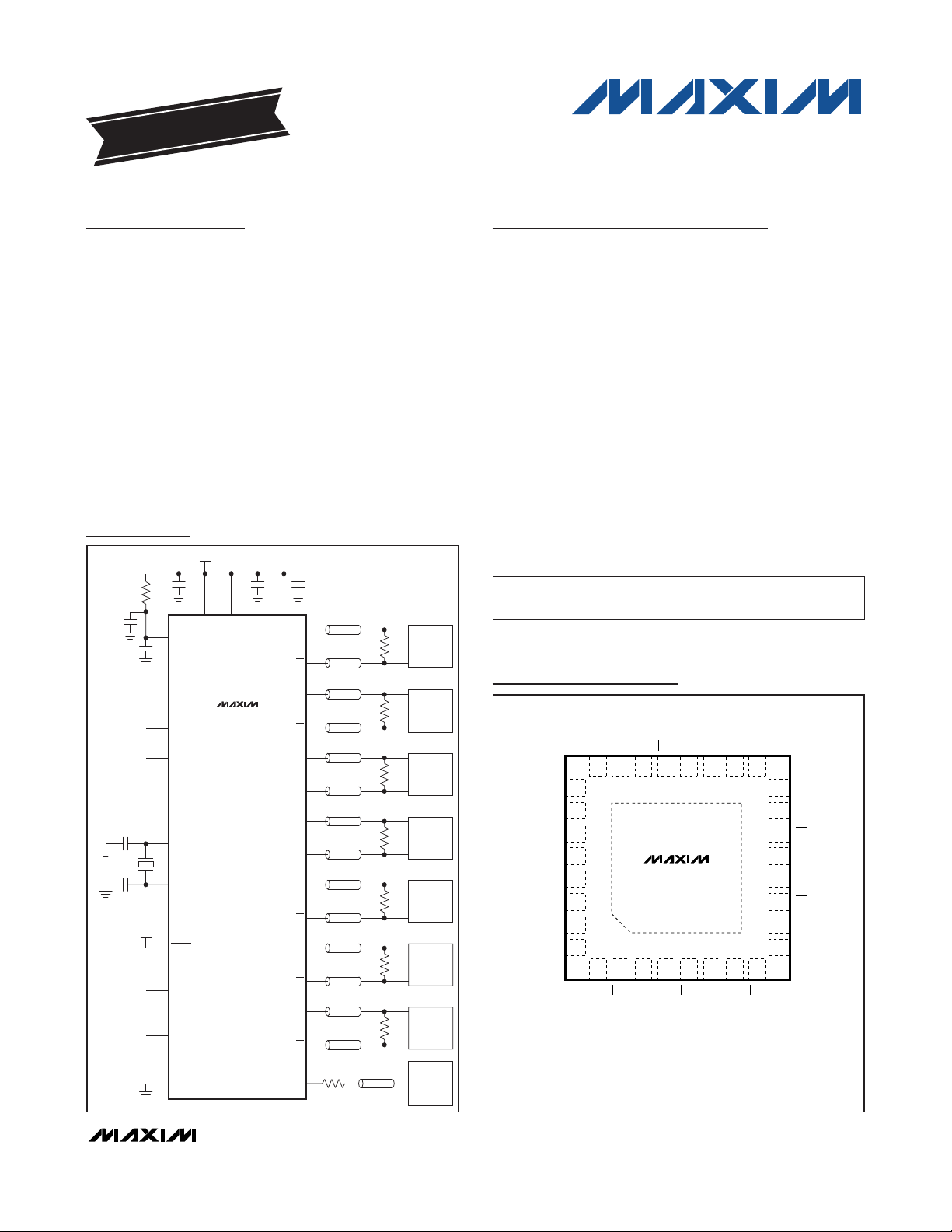
Typical Operating Circuit
+
Denotes a lead(Pb)-free/RoHS-compliant package.
*
EP = Exposed pad.
10.5Ω
10μF
0.01μF
33pF
25MHz
= 18pF)
(C
L
27pF
V
DDA
OPEN
OSC_IN
OEOPEN
X_OUT
X_IN
V
DD
PLL_BP
FSELAGND, OPEN, OR V
DD
FSELBGND, OPEN, OR V
DD
GND
+3.3V ±5%
0.1μF
0.1μF0.1μF
V
V
DDO_DIFF
DD
MAX3627
V
DDO_SE
125MHz/156MHz/312.5MHz
Q0
Q0
125MHz/156MHz/312.5MHz
Q1
Q1
125MHz/156MHz/312.5MHz
Q2
Q2
125MHz/156MHz/312.5MHz
Q3
Q3
125MHz/156MHz/312.5MHz
Q4
Q4
125MHz/156MHz/312.5MHz
Q5
Q5
125MHz/156MHz/312.5MHz
Q6
Q6
Q7
33Ω
Z0 = 50Ω
Z0 = 50Ω
Z
= 50Ω
0
Z0 = 50Ω
Z
= 50Ω
0
Z0 = 50Ω
= 50Ω
Z
0
Z0 = 50Ω
Z
= 50Ω
0
Z0 = 50Ω
Z
= 50Ω
0
Z0 = 50Ω
Z0 = 50Ω
Z0 = 50Ω
125MHz/156.25MHz
Z0 = 50Ω
100Ω
100Ω
100Ω
100Ω
100Ω
100Ω
100Ω
ASIC
ASIC
ASIC
ASIC
ASIC
ASIC
ASIC
ASIC
PART TEMP RANGE PIN-PACKAGE
MAX3627CTJ + 0°C to +70°C 32 TQFN-EP*
Page 2
MAX3627
+3.3V, Low-Jitter, Precision Clock
Generator with Multiple Outputs
2 _______________________________________________________________________________________
ABSOLUTE MAXIMUM RATINGS
ELECTRICAL CHARACTERISTICS
(VDD= +3.0V to +3.6V, TA= 0°C to +70°C, unless otherwise noted. Typical values are at VDD= +3.3V, TA= +25°C, unless otherwise
noted. When using X_IN, X_OUT input, no signal is applied at OSC_IN. When PLL is enabled, PLL_BP = high-Z or high. When PLL is
bypassed, PLL_BP = low.) (Note 1)
Stresses beyond those listed under “Absolute Maximum Ratings” may cause permanent damage to the device. These are stress ratings only, and functional
operation of the device at these or any other conditions beyond those indicated in the operational sections of the specifications is not implied. Exposure to
absolute maximum rating conditions for extended periods may affect device reliability.
Supply Voltage Range at VDD, V
DDA
,
V
DDO_SE
, V
DDO_DIFF
................................................
-0.3V to +4.0V
Voltage Range at Q0, Q0, Q1, Q1, Q2, Q2,
Q3, Q3, Q4, Q4, Q5, Q5, Q6, Q6, Q7,
PLL_BP, FSELA, FSELB, OE, OSC_IN ...-0.3V to (V
DD
+ 0.3V)
Voltage Range at X_IN ..........................................-0.3V to +1.2V
Voltage Range at X_OUT
.................................
-0.3V to (VDD- 0.6V)
Continuous Power Dissipation (T
A
= +70°C)
32-Pin TQFN-EP (derate 34.5mW/°C above +70°C)..2759mW
Operating Junction Temperature Range...........-55°C to +150°C
Storage Temperature Range .............................-65°C to +160°C
PARAMETER SYMBOL CONDITIONS MIN TYP MAX UNITS
Power-Supply Current (Note 2) I
LVDS OUTPUTS (Q0, Q0, Q1, Q1, Q2, Q2, Q3, Q3, Q4, Q4, Q5, Q5, Q6, Q6)
Output High Voltage V
Output Low Voltage V
Differentia l Output Voltage
Ampl itude
Change in Magnitude of
Differentia l Output for
Complementar y State s
Output Offset Voltage VOS 1.125 1.275 V
Change in Magnitude of Output
Offset Voltage for
Complementar y State s
Differentia l Output Impedance 80 105 140
Output Current
Cloc k Output Ri se/Fall Time tr, tf 20% to 80%, RL = 100 100 200 330 ps
Output Duty-Cycle Distortion
LVCMOS/LVTTL OUTPUT (Q7)
Output Frequency 160 MHz
Output High Voltage VOH IOH = -12mA 2.6 VDD V
Output Low Voltage VOL IOL = 12mA 0.4 V
Output Rise/Fall Time tr, tf 20% to 80% at 125MHz (Note 5) 0.15 0.4 0.8 ns
Output Duty-Cycle Distortion
Output Impedance R
PLL enabled 190 256
PLL bypassed 175
1.475 V
0.925 V
OL
| Figure 1 250 400 mV
| 25 mV
OD
| 25 mV
OS
Shorted together 5
Short to ground (Note 3) 8
PLL enabled 48 50 52
PLL bypassed (Note 4) 46 50 54
PLL enabled 46 50 54
PLL bypassed (Note 4) 45 50 55
15
|V
|V
|V
DD
OH
OD
OUT
mA
mA
%
%
Page 3
MAX3627
+3.3V, Low-Jitter, Precision Clock
Generator with Multiple Outputs
_______________________________________________________________________________________ 3
ELECTRICAL CHARACTERISTICS (continued)
(VDD= +3.0V to +3.6V, TA= 0°C to +70°C, unless otherwise noted. Typical values are at VDD= +3.3V, TA= +25°C, unless otherwise
noted. When using X_IN, X_OUT input, no signal is applied at OSC_IN. When PLL is enabled, PLL_BP = high-Z or high. When PLL is
bypassed, PLL_BP = low.) (Note 1)
INPUT SPECIFICATIONS (FSELA, FSELB, PLL_BP, OE)
Input-Voltage High VIH 2.0 VDD V
Input-Voltage Low V
Input High Current I
Input Low Current I
LVCMOS/LVTTL INPUT SPECIFICATIONS (OSC_IN) (Note 6)
Input Clock Frequenc y
Input Amplitude Range (Note 7) 1.2 3.6 V
Input High Current IIH VIN = VDD 80 μA
Input Low Current IIL VIN = 0 -80 μA
Reference Clock Dut y Cycle 40 50 60 %
Input Capacitance CIN 1.5 pF
CLOCK OUTPUT AC SPECIFICATIONS
VCO Center Frequency 625 MHz
Output Frequency with PLL
Enabled (Q0)
Output Frequency with PLL
Enabled (Q1 to Q7)
Output Frequency with PLL
Disabled
Integrated Phase Jitter RJ
Power-Supply Noise Rejection
(Note 11)
Deterministic Jitter Due to
Supply Noise (Note 12)
Nonharmonic and Subharmonic
Spurs
LVDS Clock Output SSB Phase
Noise at 125MHz (Note 14)
PARAMETER SYMBOL CONDITIONS MIN TYP MAX UNITS
0 0.8 V
IL
IH
IL
RMS
PSNR
VIN = V
DD
VIN = 0 -80 μA
PLL enabled 25
PLL bypassed 20 320
FSELA = GND 125
FSELA = VDD 156.25
FSELA = high-Z 312.5
FSELB = GND 125
FSELB = VDD 156.25
FSELB = high-Z (Note 8) 312.5
LVDS outputs 20 320
LVCMOS output 20 160
12kHz to 20MHz, PLL_BP = high (Note 9) 0.4 1.0
12kHz to 20MHz, PLL_BP = high-Z
(Note 10)
LVDS outputs -64
LVCMOS output -49
LVDS outputs 2.5
LVCMOS output 18
(Note 13) -70 dBc
f = 100Hz -115
f = 1kHz -124
f = 10kHz -126
f = 100kHz -130
f = 1MHz -143
f > 10MH z -149
80 μA
MHz
MHz
MHz
MHz
ps
0.4
RMS
dBc
ps
P-P
dBc/Hz
Page 4
MAX3627
+3.3V, Low-Jitter, Precision Clock
Generator with Multiple Outputs
4 _______________________________________________________________________________________
ELECTRICAL CHARACTERISTICS (continued)
(VDD= +3.0V to +3.6V, TA= 0°C to +70°C, unless otherwise noted. Typical values are at VDD= +3.3V, TA= +25°C, unless otherwise
noted. When using X_IN, X_OUT input, no signal is applied at OSC_IN. When PLL is enabled, PLL_BP = high-Z or high. When PLL is
bypassed, PLL_BP = low.) (Note 1)
Note 1: A series resistor of up to 10.5Ω is allowed between V
DD
and V
DDA
for filtering supply noise when system power-supply tol-
erance is V
DD
= 3.3V ±5%. See Figure 4.
Note 2: All outputs unloaded.
Note 3: The current when an LVDS output is shorted to ground is the steady-state current after the detection circuitry has settled. It
is expected that the LVDS output short to ground condition is short-term only.
Note 4: Measured with OSC_IN input with 50% duty cycle.
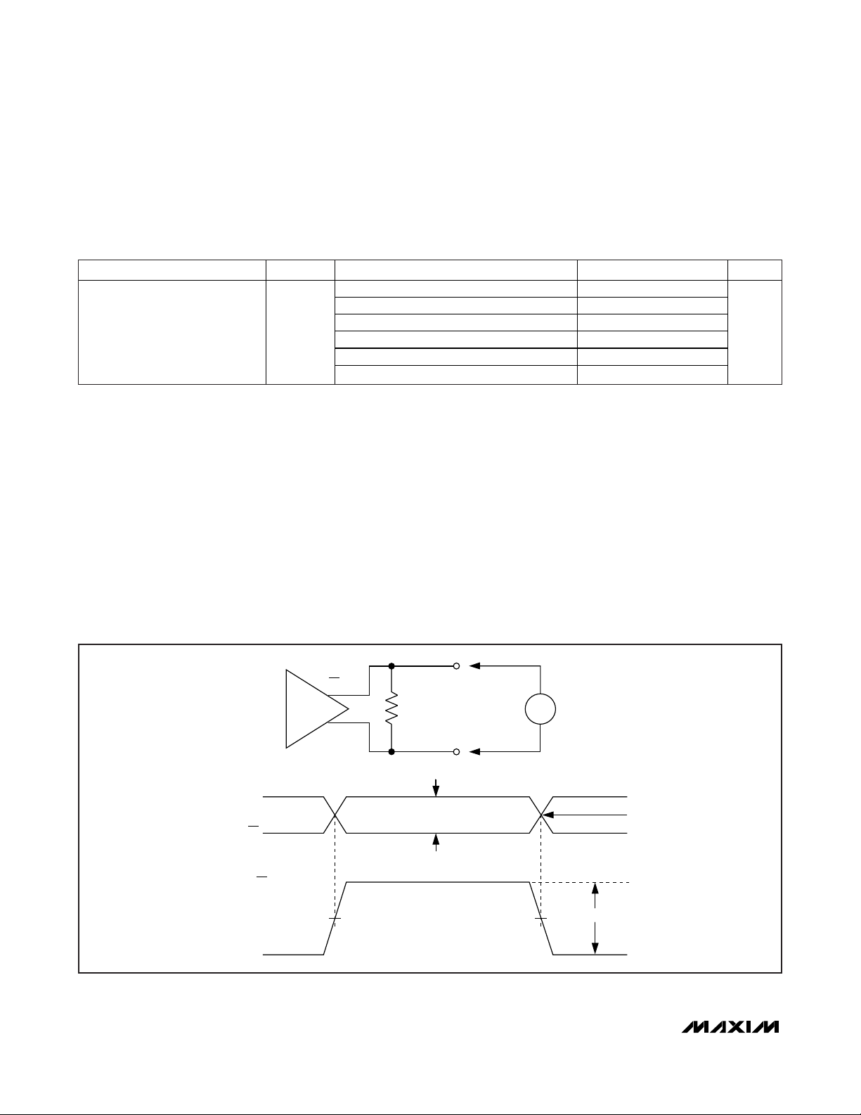
Note 5: Measured with a series resistor of 33Ω to a load capacitance of 3.0pF. See Figure 2.
Note 6: The OSC_IN input can be DC- or AC-coupled.
Note 7: Must be within the absolute maximum rating of V
DD
+ 0.3V.
Note 8: AC characteristics of LVCMOS output (Q7) are only guaranteed up to 160MHz.
Note 9: Measured with 25MHz crystal (with OSC_IN left open).
Note 10: Measured with 25MHz reference clock applied to OSC_IN.
Note 11: Measured with 40mV
P-P
sinusoidal signal on the supply at 100kHz. For LVDS the output frequency is 156.25MHz; for
LVCMOS the output frequency is 125MHz. Measured with a 10.5Ω resistor between V
DD
and V
DDA
.
Note 12: Parameter calculated based on PSNR.
Note 13: Measurement includes XTAL oscillator feedthrough, crosstalk, intermodulation spurs, etc.
Note 14: Measured with 25MHz XTAL oscillator.
Figure 1. Driver Output Levels
PARAMETER SYMBOL CONDITIONS MIN TYP MAX UNITS
f = 100Hz -113
LVCMOS Clock Output SSB
Phase Noise at 125MHz
(Note 14)
f = 1kHz -123
f = 10kHz -126
f = 100kHz -130
f = 1MHz -144
f > 10MH z -151
dBc/Hz
Qx
= 100Ω
Qx
SINGLE-ENDED OUTPUT
Qx
R
L
Qx
IV
I
OD
V
V
OD
V
OH
V
OS
V
OL
Qx - Qx
V
= 2IVODI
OD
DIFFERENTIAL OUTPUT
P-P
0
Page 5

MAX3627
+3.3V, Low-Jitter, Precision Clock
Generator with Multiple Outputs
_______________________________________________________________________________________ 5
Figure 2. LVCMOS Output Measurement Setup
Typical Operating Characteristics
(Typical values are at VDD= +3.3V, TA= +25°C, crystal frequency = 25MHz.)
V
CC
3pF
800Ω
800Ω
50Ω
MAX3627
33Ω
Q7
Z0 = 50Ω
SUPPLY CURRENT
vs. TEMPERATURE
300
275
250
225
200
175
150
125
100
SUPPLY CURRENT (mA)
75
50
25
0
070
PLL_BP = HIGH
PLL_BP = LOW
605030 402010
AMBIENT TEMPERATURE (°C)
-80
-90
MAX3627 toc01
-100
-110
-120
-130
-140
NOISE POWER DENSITY (dBc/Hz)
-150
-160
PHASE NOISE AT 125MHz
CLOCK FREQUENCY (Q0)
0.1 100,000
OFFSET FREQUENCY (kHz)
0.1μF
10,00010001 10 100
Z0 = 50Ω
-80
-90
MAX3627 toc02
-100
-110
-120
-130
-140
NOISE POWER DENSITY (dBc/Hz)
-150
-160
0.1 100,000
OSCILLOSCOPE
50Ω
PHASE NOISE AT 125MHz
CLOCK FREQUENCY (Q7)
MAX3627 toc03
10,00010001 10 100
OFFSET FREQUENCY (kHz)
Page 6

MAX3627
+3.3V, Low-Jitter, Precision Clock
Generator with Multiple Outputs
6 _______________________________________________________________________________________
Typical Operating Characteristics (continued)
(Typical values are at VDD= +3.3V, TA= +25°C, crystal frequency = 25MHz.)
PHASE NOISE AT 156.25MHz
CLOCK FREQUENCY (Q0)
-80
-90
-100
-110
-120
-130
-140
NOISE POWER DENSITY (dBc/Hz)
-150
-160
0.1 100,000
OFFSET FREQUENCY (kHz)
DIFFERENTIAL OUTPUT WAVEFORM
AT 125MHz (LVDS OUTPUT)
100mV/div
10,00010001 10 100
MAX3627 toc07
-80
-90
MAX3627 toc04
-100
-110
-120
-130
-140
NOISE POWER DENSITY (dBc/Hz)
-150
-160
0.1 100,000
DIFFERENTIAL OUTPUT WAVEFORM
100mV/div
PHASE NOISE AT 156.25MHz
CLOCK FREQUENCY (Q7)
10,00010001 10 100
OFFSET FREQUENCY (kHz)
AT 156.25MHz (LVDS OUTPUT)
MAX3627 toc08
-80
-90
MAX3627 toc05
-100
-110
-120
-130
-140
NOISE POWER DENSITY (dBc/Hz)
-150
-160
0.1 100,000
DIFFERENTIAL OUTPUT WAVEFORM
100mV/div
PHASE NOISE AT 312.5MHz
CLOCK FREQUENCY (Q0)
10,00010001 10 100
OFFSET FREQUENCY (kHz)
AT 312.5MHz (LVDS OUTPUT)
MAX3627 toc09
MAX3627 toc06
15mV/div
1ns/div
OUTPUT WAVEFORM
AT 125MHz (CMOS OUTPUT)
MEASURED USING
SETUP IN FIGURE 2
1ns/div
MAX3627 toc10
SPURS INDUCED BY POWER-SUPPLY
NOISE vs. NOISE FREQUENCY
0
fC = 156.25MHz
-10
-20
-30
-40
-50
-60
-70
SPUR AMPLITUDE (dBc)
-80
-90
-100
V
NOISE
10 1000
1ns/div
V
= 200mV
NOISE
= 100mV
P-P
V
= 40mV
NOISE
100
NOISE FREQUENCY (kHz)
SPURS INDUCED BY POWER-SUPPLY
NOISE vs. NOISE FREQUENCY
0
fC = 125MHz
OUTPUT = Q7
-10
MAX3627 toc11
-20
P-P
P-P
-30
-40
-50
-60
V
= 40mV
SPUR AMPLITUDE (dBc)
NOISE
-70
-80
-90
10 1000
NOISE FREQUENCY (kHz)
500ps/div
V
NOISE
P-P
V
100
= 200mV
= 100mV
NOISE
P-P
MAX3627 toc12
P-P
Page 7

MAX3627
+3.3V, Low-Jitter, Precision Clock
Generator with Multiple Outputs
_______________________________________________________________________________________ 7
Pin Description
PIN NAME FUNCTION
1 Q0 LVDS, Noninverting Cloc k Output
2 Q0 LVDS, Inverting Clock Output
3, 9, 24, 32 GND Supply Ground
4 Q1 LVDS, Noninverting Cloc k Output
5 Q1 LVDS, Inverting Clock Output
6, 12, 19 V
7 Q2 LVDS, Noninverting Cloc k Output
8 Q2 LVDS, Inverting Clock Output
10 Q3 LVDS, Noninverting Clock Output
11 Q3 LVDS, Inverting Clock Output
13 Q4 LVDS, Noninverting Clock Output
14 Q4 LVDS, Inverting Clock Output
15 FSELB
16 OE
17 Q5 LVDS, Noninverting Clock Output
18 Q5 LVDS, Inverting Clock Output
20 Q6 LVDS, Noninverting Clock Output
21 Q6 LVDS, Inverting Clock Output
22 V
23 Q7 LVCMOS Clock Output
25 VDD Core Power Supply. Connect to +3.3V.
26 PLL_BP
27 V
28 FSELA
29 OSC_IN
30 X_IN Crystal Osc il lator Input
31 X_OUT Crystal Oscillator Output
— EP Exposed Pad. Connect to GND for proper electrical and thermal performance.
DDO_D IFF
DDO_ SE
Power Supply for Q0, Q1, Q2, Q3, Q4, Q5, and Q6 Clock Outputs. Connect to +3.3V.
Three-State LVCMOS/LVTTL Input. Controls the Q1 to Q7 output divider. When connected to logiclow, the output frequency is 125MHz. When connected to logic-high, the output frequency is
156.25MHz. When left open (high-Z), the output frequency is 312.5MHz. For the Q7 LVCMOS output,
the output specification is only valid up to 160MHz.
LVCMOS/LVTTL Input. Enable/disable control for the Q4, Q5, and Q6 outputs. The OE pin has an
internal 75k pullup resistor. When OE is connected to V
When OE is connected to GND, Q4, Q5, and Q6 are disabled to reduce power consumption. When
disabled, Q4, Q5, and Q6 are high impedance.
Power Supply for Q7 Clock Output. Connect to +3.3V.
Three-State LVCMOS/LVTTL Input (Active Low). When connected to logic-high, the PLL lock s to the
crystal interface (25MHz typical at X_IN and X_OUT). When left open (high-Z), the PLL locks to the
OSC_IN input (25MHz typical). When connected to logic-low, the PLL is bypassed and the OSC_IN
input is selected. When bypas s mode i s selected, the VCO/PLL i s disabled to sa ve power and
eliminate intermodulation spurs.
DDA
Analog Power Supply for the VCO. Connect to +3.3V. For additional power-supply noise filtering, this
pin can be connected to V
Three-State LVCMOS/LVTTL Input. Controls the Q0 output div ider. When connected to logic-low, the
output frequenc y is 125MHz. When connected to logic-high, the output frequency is 156.25MHz.
When left open (high-Z), the output frequency is 312.5MHz.
LVCMOS Input. Self-biased to allow AC- or DC-coupling. When PLL_BP is open, the OSC_IN input
frequency should be 25MHz. When the PLL is in bypass mode (PLL_B P = low), the OSC_IN input
frequency can be between 20MHz and 320MHz. When PLL_BP is high, the OSC_IN should be
disconnected.
through a 10.5 resi stor as shown in Figure 4.
DD
or left open, Q4, Q5, and Q6 are enabled.
DD
Page 8

MAX3627
+3.3V, Low-Jitter, Precision Clock
Generator with Multiple Outputs
8 _______________________________________________________________________________________
Figure 3. Functional Diagram
OSC_IN
X_IN
OSCILLATOR
X_OUT
CMOS
CRYSTAL
0/OPEN
1
V
DD
PFD FILTER
DIVIDE
25
DDA
VCO
FSELA
DIVIDER
5, 4, OR 2
DIVIDER
5, 4, OR 2
PLL_BPV
PLL_BP
LOGIC
0
1/OPEN
0
1/OPEN
V
DDO_DIFF
125MHz/156.25MHz/
312.5MHz
LVDS
BUFFER
LVDS
BUFFER
LVDS
BUFFER
LVDS
BUFFER
LVDS
BUFFER
Q0
Q0
Q1
Q1
Q2
Q2
Q3
Q3
Q4
Q4
MAX3627
FSELB
BUFFER
BUFFER
LVCMOS
BUFFER
125MHz/156.25MHz
V
LVDS
LVDS
DDO_SEOE
Q5
Q5
Q6
Q6
Q7
Page 9

MAX3627
+3.3V, Low-Jitter, Precision Clock
Generator with Multiple Outputs
_______________________________________________________________________________________ 9
Detailed Description
The MAX3627 is a frequency generator designed to
operate at Ethernet frequencies. It consists of an onchip crystal oscillator, PLL, LVCMOS output buffer, and
LVDS output buffers. Using a low-frequency clock
(crystal or CMOS input) as a reference, the internal PLL
generates a high-frequency output clock with excellent
jitter performance. The outputs can be switched among
125MHz, 156.25MHz, and 312.5MHz.
Crystal Oscillator
An integrated oscillator provides the low-frequency reference clock for the PLL. This oscillator requires an
external crystal connected between X_IN and X_OUT.
The crystal frequency is 25MHz. See the
Applications
Information
section for more information.
OSC_IN Buffer
The LVCMOS OSC_IN buffer is internally biased to
allow AC- or DC-coupling. This input is internally ACcoupled, and is designed to operate at 25MHz when
the PLL is enabled (PLL_BP is left open). When the PLL
is bypassed (PLL_BP is set low), the OSC_IN buffer can
be operated from 20MHz to 320MHz.
PLL
The PLL takes the signal from the crystal oscillator or
reference clock input and synthesizes a low-jitter, highfrequency clock. The PLL contains a phase-frequency
detector (PFD), a lowpass filter, and a voltage-controlled oscillator (VCO) that operates at 625MHz. The
PLL bandwidth is tuned to 150kHz typical to optimize
both phase noise and power-supply noise rejection
(PSNR). The VCO output is connected to the PFD input
through a feedback divider that divides the VCO frequency by 25 to lock onto the 25MHz reference clock
or oscillator. For output Q0, the FSELA pin is used to
select among 125MHz, 156.25MHz, and 312.5MHz. For
outputs Q1 to Q6, the FSELB pin is used to select
among 125MHz, 156.25MHz, and 312.5MHz. For the
Q7 output, the FSELB pin is used to select between
125MHz and 156.25MHz. To minimize the jitter induced
by power-supply noise, the VCO supply (V
DDA
) is iso-
lated from the core logic and output buffer supplies.
LVDS Drivers
The high-frequency outputs—Q0, Q1, Q2, Q3, Q4, Q5,
and Q6—are differential LVDS buffers designed to
drive 100Ω.
LVCMOS Driver
LVCMOS output Q7 is provided on the MAX3627. It is
designed to drive single-ended high-impedance loads.
The output specifications are only valid up to 160MHz.
Applications Information
Power-Supply Filtering
The MAX3627 is a mixed analog/digital IC. The PLL
contains analog circuitry susceptible to random noise.
To take full advantage of on-board filtering and noise
attenuation, in addition to excellent on-chip power-supply rejection, this part provides a separate power-supply pin, V
DDA
, for the VCO circuitry. The purpose of this
design technique is to ensure clean input power supply
to the VCO circuitry and to improve the overall immunity
to power-supply noise. Figure 4 illustrates the recommended power-supply filter network for V
DDA
. This network requires that the power supply is +3.3V ±5%.
Decoupling capacitors should be used on all other supply pins and placed as close as possible to the pins for
best performance.
Crystal Input Layout
and Frequency Stability
The MAX3627 features an integrated on-chip crystal
oscillator to minimize system implementation cost. The
integrated crystal oscillator is a Pierce-type that uses
the crystal in its parallel resonance mode. It is recommended to use a 25MHz crystal with a load specification of CL= 18pF. See Table 1 for the recommended
crystal specifications.
The crystal, trace, and two external capacitors should
be placed on the board as close as possible to the
X_IN and X_OUT pins to minimize the board parasitic
capacitance and prevent active signals from coupling
into the oscillator.
Figure 4. Analog Supply Filtering
+3.3V ±5%
V
DD
MAX3627
10.5Ω
V
DDA
0.01μF 10μF
0.1μF
Page 10

MAX3627
+3.3V, Low-Jitter, Precision Clock
Generator with Multiple Outputs
10 ______________________________________________________________________________________
Table 1. Crystal Selection Parameters
The layout shown in Figure 5 gives approximately 2pF
of trace plus footprint capacitance per side of the crystal (Y1). The dielectric material is FR4, and dielectric
thickness of the reference board is 15 mils. Using a
25MHz crystal and the capacitor values of C45 = 27pF
and C46 = 33pF, the measured output frequency accuracy is -1ppm at +25°C ambient temperature.
Crystal Selection
The crystal oscillator is designed to drive a fundamental
mode, AT-cut crystal resonator. See Table 1 for recommended crystal specifications. See Figure 6 for external
capacitance connection.
Figure 5. Crystal Layout
Figure 6. Crystal, Capacitors Connection
PARAMETER SYMBOL MIN TYP MAX UNITS
Crystal Oscillat ion Frequency f
Shunt Capacitance CO 7.0 pF
Load Capacitance CL 18 pF
Equivalent Series Resistance (ESR) RS 50
Max imum Crystal Drive Level 300 μW
25 MHz
OSC
27pF
X_IN
CRYSTAL
(C
= 18pF)
L
33pF
MAX3627
X_OUT
Page 11

MAX3627
+3.3V, Low-Jitter, Precision Clock
Generator with Multiple Outputs
Maxim cannot assume responsibility for use of any circuitry other than circuitry entirely embodied in a Maxim product. No circuit patent licenses are
implied. Maxim reserves the right to change the circuitry and specifications without notice at any time.
Maxim Integrated Products, 120 San Gabriel Drive, Sunnyvale, CA 94086 408-737-7600 ____________________
11
© 2009 Maxim Integrated Products Maxim is a registered trademark of Maxim Integrated Products, Inc.
Interface Models
Figures 7, 8, and 9 show examples of interface models.
Layout Considerations
The inputs and outputs are the most critical paths for
the MAX3627 and great care should be taken to minimize discontinuities on these transmission lines
between the connector and the IC. Here are some suggestions for maximizing the performance of the
MAX3627:
• An uninterrupted ground plane should be positioned beneath the clock outputs. The ground
plane under the crystal should be removed to minimize capacitance.
• Ground pin vias should be placed close to the IC
and the input/output interfaces to allow a return
current path to the MAX3627 and the receive
devices.
• Supply decoupling capacitors should be placed
close to the supply pins, preferably on the same
layer as the MAX3627.
• Take care to isolate crystal input traces from the
MAX3627 outputs.
• The crystal, trace, and two external capacitors
should be placed on the board as close as possible to the X_IN and X_OUT pins.
• Maintain 100Ω differential (or 50Ω single-ended)
transmission line impedance into and out of the part.
• Use good high-frequency layout techniques and
multilayer boards with an uninterrupted ground
plane to minimize EMI and crosstalk.
Refer to the MAX3627 evaluation kit for more information.
Exposed-Pad Package
The exposed pad on the 32-pin TQFN package provides a very low inductance path for return current traveling to the PCB ground plane. The pad is thermal and
electrical ground on the MAX3627 and must be soldered to the circuit board ground for proper electrical
performance.
Chip Information
PROCESS: BiCMOS
Figure 7. Simplified OSC_IN Pin Circuit Schematic
Figure 8. Simplified LVCMOS Output Circuit Schematic
Figure 9. Simplified OE Pin Circuit Schematic
Package Information
For the latest package outline information and land patterns, go
to www.maxim-ic.com/packages
.
PACKAGE TYPE PACKAGE CODE DOCUMENT NO.
32 TQFN-EP T3255+5
21-0140
1.4V
V
DD
180kΩ
OSC_IN
ESD
STRUCTURES
V
DDO_SE
10Ω
Q7
10Ω
ESD
STRUCTURES
V
DDO_DIFF
OE
V
DD
75kΩ
ESD
STRUCTURES
 Loading...