

Page 1
MAX3625B
Low-Jitter, Precision Clock
Generator with Three Outputs
________________________________________________________________
Maxim Integrated Products
1
19-4978; Rev 0; 10/09
For pricing, delivery, and ordering information, please contact Maxim Direct at 1-888-629-4642,
or visit Maxim’s website at www.maxim-ic.com.
EVALUATION KIT
AVAILABLE
General Description
The MAX3625B is a low-jitter, precision clock generator
optimized for networking applications. The device integrates a crystal oscillator and a phase-locked loop
(PLL) clock multiplier to generate high-frequency clock
outputs for Ethernet, 10G Fibre Channel, and other networking applications.
Maxim’s proprietary PLL design features ultra-low jitter
and excellent power-supply noise rejection, minimizing
design risk for network equipment.
The MAX3625B has three LVPECL outputs. Selectable
output dividers and a selectable feedback divider allow
a range of output frequencies.
Applications
Ethernet Networking Equipment
Fibre Channel Storage Area Network
Features
♦ Crystal Oscillator Interface: 24.8MHz to 27MHz
♦ CMOS Input: Up to 320MHz
♦ Output Frequencies
Ethernet: 62.5MHz, 125MHz, 156.25MHz, 312.5MHz
10G Fibre Channel: 159.375MHz, 318.75MHz
♦ Low Jitter
0.14ps
RMS
(1.875MHz to 20MHz)
0.36ps
RMS
(12kHz to 20MHz)
♦ Excellent Power-Supply Noise Rejection
♦ No External Loop Filter Capacitor Required
Ordering Information
CRYSTAL
OSCILLATOR
LVCMOS
DIVIDERS:
M = 24, 25
NA = 10, 2, 4, 5
NB = 10, 2, 4, 5
REF_IN
X_IN
X_OUT
0
1
0
1
PFD FILTER
RESET
RESET
RESET LOGIC/POR
DIVIDER
M
RESET
DIVIDER
NB
DIVIDER
NA
VCO
620MHz TO 648MHz
LVPECL
BUFFER
QA
QA_OE
QA
LVPECL
BUFFER
QB1
QB1
LVPECL
BUFFER
QB0
FB_SEL
QB_OE
QB0
SELB[1:0]
SELA[1:0]IN_SEL
BYPASSMR
MAX3625B
SELA[1:0]
RESET
SELB[1:0]
FB_SEL
BYPASS
33pF
27pF
Block Diagram
+
Denotes a lead(Pb)-free/RoHS-compliant package.
*
EP = Exposed pad.
Typical Application Circuit appears at end of data sheet.
PART TEMP RANGE PIN-PACKAGE
MAX3625BEUG+ -40°C to +85°C 24 TSSOP-EP*
Page 2
MAX3625B
Low-Jitter, Precision Clock
Generator with Three Outputs
2 _______________________________________________________________________________________
ABSOLUTE MAXIMUM RATINGS
ELECTRICAL CHARACTERISTICS
(VCC= +3.0V to +3.6V, TA= -40°C to +85°C, unless otherwise noted. Typical values are at VCC= +3.3V, TA= +25°C, unless otherwise noted.) (Notes 1, 2)
Stresses beyond those listed under “Absolute Maximum Ratings” may cause permanent damage to the device. These are stress ratings only, and functional
operation of the device at these or any other conditions beyond those indicated in the operational sections of the specifications is not implied. Exposure to
absolute maximum rating conditions for extended periods may affect device reliability.
Supply Voltage Range VCC, V
CCA
,
V
CCO_A
, V
CCO_B
..............................................-0.3V to +4.0V
Voltage Range at REF_IN, IN_SEL,
FB_SEL, SELA[1:0], SELB[1:0],
QA_OE, QB_OE, MR, BYPASS ..............-0.3V to (V
CC
+ 0.3V)
Voltage Range at X_IN ..........................................-0.3V to +1.2V
Voltage Range at X_OUT ............................-0.3V to (V
CC
- 0.6V)
Current into QA, QA, QB0, QB0, QB1, QB1 .....................-56mA
Continuous Power Dissipation (T
A
= +70°C)
24-Pin TSSOP (derate 26.7mW/°C above +70°C) ..2133.3mW
Operating Junction Temperature Range...........-55°C to +150°C
Storage Temperature Range .............................-65°C to +160°C
PARAMETER SYMBOL CONDITIONS MIN TYP MAX UNITS
Power-Supply Current (Note 3) I
CONTROL INPUT CHARACTERISTICS
(SELA[1:0], SELB[1:0], FB_SEL, IN _SEL, QA_OE, QB_OE, MR, B Y PA SS Pins)
Input Capacitance C
Input Pulldown Resistor R
Input Logic Bia s Resistor R
Input Pullup Resistor R
LVPECL OUTPUTS (QA, QA, QB0, QB0, QB1, QB1 Pins)
Output High Voltage V
Output Low Voltage V
Peak-to-Peak Output-Voltage
Swing (Single-Ended)
Cloc k Output Rise/Fall Time 20% to 80% (Note 2) 200 350 600 ps
Output Duty-Cycle Distortion
LVCMOS/LVTTL INPUTS
(SELA[1:0], SELB[1:0], FB_SEL, IN _SEL, QA_OE, QB_OE, MR, B Y PA SS Pins)
Input-Voltage High VIH 2.0 V
Input-Voltage Low V
Input High Current I
Input Low Current I
CC
PULLDOWN
BIAS
PULLUP
OH
OL
IH
IN_SEL = high 72 98
IN_SEL = low 74
2 pF
IN
Pins MR, FB_SEL 75 k
Pins SELA[1:0], SELB[1:0] 50 k
Pins QA_OE, QB_OE, IN_SEL, BYPASS 75 k
(Note 2) 0.6 0.72 0.9 V
PLL enabled 48 50 52
PLL bypassed (Note 4) 45 50 55
0.8 V
IL
VIN = V
CC
VIN = 0V -80 μA
IL
VCC -
1.18
VCC -
1.90
VCC -
0.98
VCC -
1.7
80 μA
VCC -
0.83
VCC -
1.55
mA
V
V
P-P
%
Page 3
MAX3625B
Low-Jitter, Precision Clock
Generator with Three Outputs
_______________________________________________________________________________________ 3
ELECTRICAL CHARACTERISTICS (continued)
(VCC= +3.0V to +3.6V, TA= -40°C to +85°C, unless otherwise noted. Typical values are at VCC= +3.3V, TA= +25°C, unless otherwise noted.) (Notes 1, 2)
Note 1: A series resistor of up to 10.5Ω is allowed between VCCand V
CCA
for filtering supply noise when system power-supply
tolerance is V
CC
= 3.3V ±5%. See Figure 1.
Note 2: LVPECL outputs guaranteed up to 320MHz.
Note 3: All outputs enabled and unloaded.
Note 4: Measured with a crystal (see Table 4) or an AC-coupled, 50% duty-cycle signal on REF_IN.
Note 5: Measured with crystal source, see Table 4.
Note 6: Measured using setup shown in Figure 1.
Note 7: Measured with 40mV
P-P
, 100kHz sinusoidal signal on the supply.
Note 8: Measured at 156.25MHz output.
Note 9: Calculated based on measured spurs induced by power-supply noise (refer to Application Note 4461:
HFAN-04.5.5:
Characterizing Power-Supply Noise Rejection in PLL Clock Synthesizers
).
Note 10: Measured with 25MHz crystal or 25MHz reference clock at REF_IN with a slew rate of 0.5V/ns or greater.
PARAMETER SYMBOL CONDITIONS MIN TYP MAX UNITS
REF_IN SPECIFICATIONS (Input DC- or AC-Coupled)
Reference Clock Frequenc y
Input-Voltage High VIH 2.0 V
Input-Voltage Low V
Input High Current I
Input Low Current I
Reference Clock Duty Cycle PLL enabled 30 70 %
Input Capacitance 2.5 pF
CLOCK OUTPUT AC SPECIFICATIONS
VCO Frequency Range 620 648 MHz
Random Jitter (Note 5) RJ
Spurs Induced by Power-Supply
Noise
Determin istic Jitter Induced by
Power-Supply Noise
Nonharmonic and Subharmonic
Spurs
Output Skew Between any output pair 5 ps
Clock Output SSB Phase Noise
at 125MH z (Note 10)
IH
RMS
PLL enabled 24.8 27.0
PLL bypassed 320
0.8 V
IL
VIN = V
CC
VIN = 0V -240 μA
IL
12kHz to 20MHz 0.36 1.0
1.875MHz to 20MHz 0.14
(Notes 6, 7, 8) -60 dBc
(Note 9) 5.6 ps
-70 dBc
f = 1kHz -124
f = 10kHz -127
f = 100kHz -131
f = 1MHz -145
f > 10MH z -153
240 μA
MHz
ps
RMS
P-P
dBc/Hz
Page 4

MAX3625B
Low-Jitter, Precision Clock
Generator with Three Outputs
4 _______________________________________________________________________________________
Typical Operating Characteristics
(Typical values are at VCC= +3.3V, TA= +25°C, crystal frequency = 25MHz.)
SUPPLY CURRENT
vs. TEMPERATURE
250
225
200
175
ALL OUTPUTS ACTIVE AND TERMINATED
150
125
100
ALL OUTPUTS ACTIVE AND UNTERMINATED
75
SUPPLY CURRENT (mA)
50
25
0
-40 85
AMBIENT TEMPERATURE (°C)
PHASE NOISE AT 125MHz
CLOCK FREQUENCY
-80
-90
-100
-110
-120
-130
-140
NOISE POWER DENSITY (dBc/Hz)
-150
-160
0.1 100,000
OFFSET FREQUENCY (kHz)
DIFFERENTIAL OUTPUT WAVEFORM
AT 156.25MHz
MAX3625B toc01
AMPLITUDE (200mv/div)
603510-15
1ns/div
MAX3625B toc02
-80
-90
-100
-110
-120
-130
-140
NOISE POWER DENSITY (dBc/Hz)
-150
-160
PHASE NOISE AT 156.25MHz
CLOCK FREQUENCY
-80
-90
MAX3625B toc04
-100
-110
-120
-130
-140
NOISE POWER DENSITY (dBc/Hz)
-150
10,00010001 10 100
-160
0.1 100,000
OFFSET FREQUENCY (kHz)
10,00010001 10 100
-10
-20
MAX3625B toc05
-30
-40
-50
-60
-70
SPUR AMPLITUDE (dBc)
-80
-90
-100
PHASE NOISE AT 312.5MHz
CLOCK FREQUENCY
0.1 100,000
OFFSET FREQUENCY (kHz)
10,00010001 10 100
SPURS INDUCED BY POWER-SUPPLY NOISE
vs. NOISE FREQUENCY
0
fC = 156.25MHz
NOISE AMPLITUDE = 40mV
10 10,000
NOISE FREQUENCY (kHz)
P-P
1000100
MAX3625B toc03
MAX3625B toc06
Page 5

MAX3625B
Low-Jitter, Precision Clock
Generator with Three Outputs
_______________________________________________________________________________________ 5
Pin Description
Pin Configuration
+
TOP VIEW
MAX3625B
TSSOP
21
4
QB0V
CCO_A
22
3
QB0MR
23
2
V
CCO_B
BYPASS
24
1
SELB1SELB0
18
7
IN_SEL
QB_OE
19
6
QB1QA
17
8
REF_INQA_OE
16
9
X_INFB_SEL
15
10
X_OUTV
CCA
14
11
GNDV
CC
13
12
SELA1SELA0
20
5
QB1
QA
*EP
*EXPOSED PAD MUST BE SOLDERED TO GROUND FOR PROPER
THERMAL AND ELECTRICAL OPERATION.
PIN NAME FUNCTION
1, 24
SELB0 ,
SELB1
LVCMOS/LVTTL Inputs. Control NB divider setting. Has 50k input impedance. See Table 2 for more
information.
LVCMOS/LVTTL Input (Active Low). Connect low to bypass the internal PLL. Connect high or leave
2
BYPASS
3 MR
4 V
CCO_ A
5 QA Nonin verting Clock Output, LVPECL
6
QA
open for normal operation. When in bypass mode the output div iders are set to divide by 1. Has
internal 75k pullup to V
LVCMOS/LVTTL Input. Master reset input. Pulse high for > 1μs to reset all dividers. Has internal 75k
CC
.
pulldown to GND. Not required for normal operation.
Power Supply for QA Cloc k Output. Connect to +3.3V.
Inverting Clock Output, LVPECL
LVCMOS/LVTTL Input. Enables/disab les QB c loc k outputs. Connect pin high or lea ve open to enable
7 QB_OE
8 QA_OE
9 FB_SEL
LVPECL c lock outputs QB0 and QB1. Con nect low to set QB0 and QB1 to a logic 0. Has interna l 75 k
pullup to V
CC
.
LVCMOS/LVTTL Input. Enables/disab les the QA clock output. Connect high or lea ve open to enable the
LVPECL c lock output QA. Connect low to set QA to a log ic 0. Has interna l 75k pullup to V
LVCMOS/LVTTL Input. Controls M divider setting. See Table 3 for more information. Has internal 75k
pulldown to GND.
.
CC
Page 6

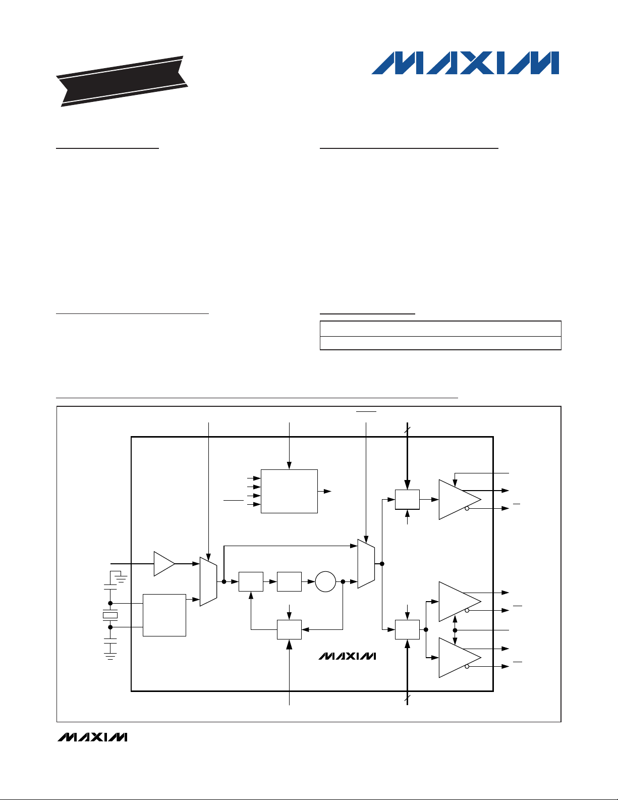
Detailed Description
The MAX3625B is a low-jitter clock generator designed
to operate at Ethernet and Fibre Channel frequencies. It
consists of an on-chip crystal oscillator, PLL, programmable dividers, and LVPECL output buffers. Using a
low-frequency clock (crystal or CMOS input) as a reference, the internal PLL generates a high-frequency output clock with excellent jitter performance.
Crystal Oscillator
An integrated oscillator provides the low-frequency reference clock for the PLL. This oscillator requires an
external crystal connected between X_IN and X_OUT.
The crystal frequency is 24.8MHz to 27MHz.
REF_IN Buffer
An LVCMOS-compatible clock source can be connected to REF_IN to serve as the reference clock.
The LVCMOS REF_IN buffer is internally biased to the
threshold voltage (1.4V typ) to allow AC- or DC-coupling, and is designed to operate up to 320MHz.
PLL
The PLL takes the signal from the crystal oscillator or
reference clock input and synthesizes a low-jitter, highfrequency clock. The PLL contains a phase-frequency
detector (PFD), a lowpass filter, and a voltage-
controlled oscillator (VCO) with a 620MHz to 648MHz
operating range. The VCO is connected to the PFD
input through a feedback divider. See Table 3 for
divider values. The PFD compares the reference frequency to the divided-down VCO output (f
VCO
/M) and
generates a control signal that keeps the VCO locked
to the reference clock. The high-frequency VCO output
clock is sent to the output dividers. To minimize noiseinduced jitter, the VCO supply (V
CCA
) is isolated from
the core logic and output buffer supplies.
Output Dividers
The output dividers are programmable to allow a range of
output frequencies. See Table 2 for the divider input settings. The output dividers are automatically set to divide by
1 when the MAX3625B is in bypass mode (BYPASS = 0).
Figure 1. Analog Supply Filtering
MAX3625B
Low-Jitter, Precision Clock
Generator with Three Outputs
6 _______________________________________________________________________________________
Pin Description (continued)
PIN NAME FUNCTION
10 V
11 VCC Core Power Supply. Connect to +3.3V.
12, 13
14 GND Supply Ground
15 X_OUT Crystal Oscillator Output
16 X_IN Crysta l Oscillator Input
17 REF_IN LVCMOS Reference Clock Input. Self-biased to allow AC- or DC-coupling.
18 IN_SEL
19
20 QB1 LVPECL, Nonin verting C lock Output
21
22 QB0 LVPECL, Nonin verting C lock Output
23 V
— EP Exposed Pad. Supply ground; connect to PCB ground for proper electrical and thermal performance.
CCA
SELA0 ,
SELA1
QB1
QB0
CCO_ B
Analog Power Supply for the VCO. Connect to +3.3V. For additional power-supply noi se fi lter ing, this
pin can connect to V
LVCMOS/LVTTL Inputs. Control NA divider setting. See Table 2 for more information. 50k input
impedance.
LVCMOS/LVTTL Input. Connect high or leave open to use a crystal. Connect low to use REF_IN. Has
internal 75k pullup to V
LVPECL, Inverting Cl oc k Output
LVPECL, Inverting Cl oc k Output
Power Supply for QB0 and QB1 Clock Output. Connect to +3.3V.
through 10.5 as shown in Figure 1 (requires VCC = 3.3V ±5%).
CC
.
CC
+3.3V ±5%
V
CC
10.5Ω
V
CCA
0.01μF 10μF
0.01μF
Page 7

MAX3625B
Low-Jitter, Precision Clock
Generator with Three Outputs
_______________________________________________________________________________________ 7
Table 1. Output Frequency Determination
LVPECL Drivers
The high-frequency outputs—QA, QB0, and QB1—are
differential PECL buffers designed to drive transmission
lines terminated with 50Ω to VCC- 2.0V. The maximum
operating frequency is specified up to 320MHz. The
outputs can be disabled, if not used. The outputs go to
a logic 0 when disabled.
Reset Logic/POR
During power-on, a power-on reset (POR) signal is generated to synchronize all dividers. An external master
reset (MR) signal is not required.
Applications Information
Power-Supply Filtering
The MAX3625B is a mixed analog/digital IC. The PLL
contains analog circuitry susceptible to random noise.
In addition to excellent on-chip power-supply noise
rejection, the MAX3625B provides a separate powersupply pin, V
CCA
, for the VCO circuitry. Figure 1 illustrates the recommended power-supply filter network for
V
CCA
. The purpose of this design technique is to
ensure a clean power supply to the VCO circuitry and
to improve the overall immunity to power-supply noise.
This network requires that the power supply is +3.3V
±5%. Decoupling capacitors should be used on all
supply pins for best performance.
Output Divider Configuration
Table 2 shows the input settings required to set the output dividers. Note that when the MAX3625B is in
bypass mode (BYPASS set low), the output dividers are
automatically set to divide by 1.
PLL Divider Configuration
Table 3 shows the input settings required to set the PLL
feedback divider.
Table 2. Output Divider Configuration
Table 3. PLL Divider Configuration
CRYSTAL OR
CMOS INPUT
FREQUENCY
(MHz)
25 25 625
25.78125 25 644.53125 4 161.132812 10Gbps Ethernet
26.04166 24 625
26.5625 24 637.5
FEEDBACK
DIVIDER, M
VCO
FREQUENCY
(MHz)
OUTPUT
DIVIDER,
NA AND NB
2 312.5
4 156.25
5 125
10 62.5
2 312.5
4 156.25
5 125
10 62.5
2 318.75
4 159.375
OUTPUT
FREQUENCY
(MHz)
APPLICATIONS
Ethernet
Ethernet
10G Fibre Channel
INPUT
SELA1/SELB1 SELA0/SELB0
0 0 ÷10
0 1 ÷2
1 0 ÷4
1 1 ÷5
NA/NB DIVIDER
FB_SEL INPUT M DIVIDER
0 ÷25
1 ÷24
Page 8

MAX3625B
Crystal Selection
The crystal oscillator is designed to drive a fundamental
mode, AT-cut crystal resonator. See Table 4 for recommended crystal specifications. See Figure 3 for external
capacitance connection.
Crystal Input Layout
The crystal, trace, and two external capacitors should
be placed on the board as close as possible to the
MAX3625B’s X_IN and X_OUT pins to reduce crosstalk
of active signals into the oscillator. The example layout
shown in Figure 2 gives approximately 3pF of trace
plus footprint capacitance per side of the crystal. The
dielectric material is FR4 and dielectric thickness of the
reference board is 15 mils. Using a 25MHz crystal and
the capacitor values of C10 = 27pF and C9 = 33pF, the
measured output frequency accuracy is -14ppm at
+25°C ambient temperature.
Interfacing with LVPECL Outputs
The equivalent LVPECL output circuit is given in Figure 7.
These outputs are designed to drive a pair of 50Ω transmission lines terminated with 50Ω to VTT= VCC- 2V. If a
separate termination voltage (V
TT
) is not available, other
termination methods can be used such as shown in
Figures 4 and 5. Unused outputs should be disabled and
may be left open. For more information on LVPECL terminations and how to interface with other logic families, refer
to Application Note 291:
HFAN-01.0: Introduction to
LVDS, PECL, and CML
.
Low-Jitter, Precision Clock
Generator with Three Outputs
8 ____________________________________________________
Figure 4. Thevenin Equivalent of Standard PECL Termination
Figure 5. AC-Coupled PECL Termination
Table 4. Crystal Selection Parameters
Figure 2. Crystal Layout
Figure 3. Crystal, Capacitors Connection
PARAMETER SYMBOL MIN TYP MAX UNITS
Crystal Oscillation
Frequency
Shunt Capacitance CO 2.0 7.0 pF
Load Capacitance CL 18 pF
Equivalent Series
Resistance (ESR)
Maximum Crystal
Dri ve Le vel
f
24.8 27 MHz
OSC
50
R
S
300 μW
+3.3V
27pF
X_IN
CRYSTAL
(C
= 18pF)
L
X_OUT
33pF
130Ω 130Ω
MAX3625B
MAX3625B
NOTE: AC-COUPLING IS OPTIONAL.
Z
Z0 = 50Ω
150Ω
= 50Ω
0
82Ω
0.1μF
0.1μF
150Ω
Z0 = 50Ω
100Ω
Z0 = 50Ω
HIGH
IMPEDANCE
82Ω
HIGH
IMPEDANCE
Qx
Qx
Qx
Qx
Page 9

Interface Models
Figures 6 and 7 show examples of interface models.
Layout Considerations
The inputs and outputs are critical paths for the
MAX3625B, and care should be taken to minimize discontinuities on these transmission lines. Here are some
suggestions for maximizing the MAX3625B’s performance:
• An uninterrupted ground plane should be positioned beneath the clock I/Os.
• Supply and ground pin vias should be placed
close to the IC and the input/output interfaces to
allow a return current path to the MAX3625B and
the receive devices.
• Supply decoupling capacitors should be placed
close to the MAX3625B supply pins.
• Maintain 100Ω differential (or 50Ω single-ended)
transmission line impedance out of the MAX3625B.
• Use good high-frequency layout techniques and
multilayer boards with an uninterrupted ground
plane to minimize EMI and crosstalk.
• The 24-pin TSSOP-EP package features an
exposed pad (EP), which provides a low-resistance thermal path for heat removal from the IC,
and must be connected to the circuit board ground
plane for proper operation.
Refer to the MAX3625B Evaluation Kit for more information.
Chip Information
TRANSISTOR COUNT: 10,840
PROCESS: BiCMOS
MAX3625B
Low-Jitter, Precision Clock
Generator with Three Outputs
_______________________________________________________________________________________ 9
Figure 7. Simplified LVPECL Output Circuit Schematic
Figure 6. Simplified REF_IN Pin Circuit Schematic
V
CC
V
= 1.4V
B
V
REF_IN
V
CC
CC
V
B
14.5kΩ
ESD
STRUCTURES
V
B
ESD
STRUCTURES
Qx
Qx
Page 10

MAX3625B
Low-Jitter, Precision Clock
Generator with Three Outputs
Maxim cannot assume responsibility for use of any circuitry other than circuitry entirely embodied in a Maxim product. No circuit patent licenses are
implied. Maxim reserves the right to change the circuitry and specifications without notice at any time.
10
____________________Maxim Integrated Products, 120 San Gabriel Drive, Sunnyvale, CA 94086 408-737-7600
© 2009 Maxim Integrated Products Maxim is a registered trademark of Maxim Integrated Products, Inc.
MAX3625B
V
CCA
REF_IN
IN_SEL
QA_OE
FB_SEL
QB_OE
BYPASS
SELA0
SELB0
SELA1
SELB1
MR
X_OUT
X_IN GND
V
CC
V
CCO_A
V
CCO_B
10.5Ω
0.01μF
V
CC
10μF
26.0416MHz
(C
L
= 18pF)
33pF 27pF
0.01μF 0.1μF
+3.3V ±5%
QA
150Ω
Z
0
= 50Ω
Z0 = 50Ω
ASIC
150Ω
312.5MHz
QA
0.1μF
0.1μF
QB0
150Ω
Z
0
= 50Ω
Z0 = 50Ω
ASIC
150Ω
156.25MHz
QB0
0.1μF
0.1μF
QB1
150Ω
Z
0
= 50Ω
Z0 = 50Ω
ASIC
150Ω
156.25MHz
QB1
0.1μF
0.1μF
Typical Application Circuit
PACKAGE TYPE PACKAGE CODE DOCUMENT NO.
24 TSSOP-EP U24E+1
21-0108
Package Information
For the latest package outline information and land patterns, go to www.maxim-ic.com/packages. Note that a “+”, “#”, or “-” in the
package code indicates RoHS status only. Package drawings may show a different suffix character, but the drawing pertains to the
package regardless of RoHS status.
 Loading...