

Page 1
MAX3622
Low-Jitter, Precision Clock Generator
with Two Outputs
________________________________________________________________
Maxim Integrated Products
1
19-2456; Rev 0; 11/07
For pricing, delivery, and ordering information, please contact Maxim Direct at 1-888-629-4642,
or visit Maxim’s website at www.maxim-ic.com.
EVALUATION KIT
AVAILABLE
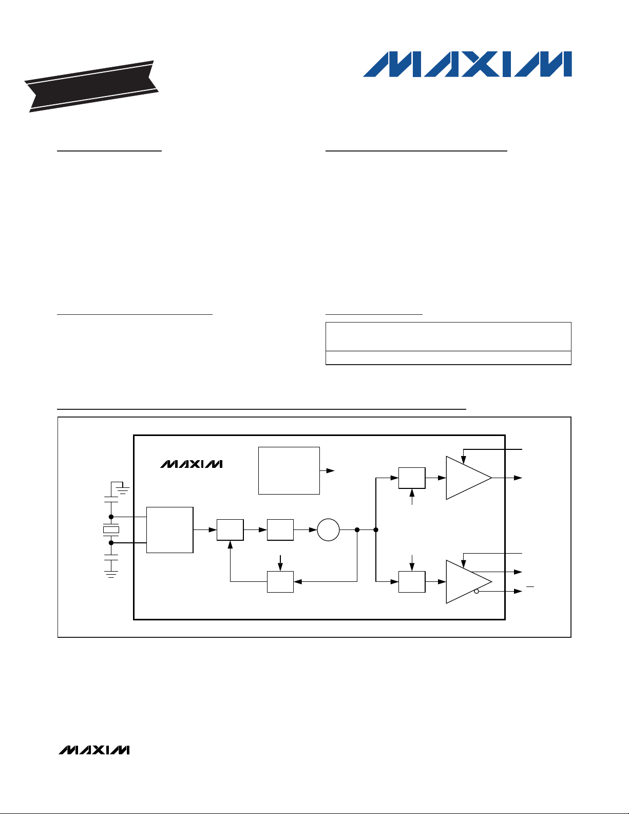
General Description
The MAX3622 is a low-jitter precision clock generator
optimized for networking applications. The device integrates a crystal oscillator and a phase-locked loop
(PLL) clock multiplier to generate high-frequency clock
outputs for Ethernet and other networking applications.
Maxim’s proprietary PLL design features ultra-low jitter
(0.36ps
RMS
) and excellent power-supply noise rejec-
tion, minimizing design risk for network equipment.
The MAX3622 has one LVPECL output and one
LVCMOS output. It is available in a 16-pin TSSOP package and operates over the 0°C to +70°C temperature
range.
Applications
Ethernet Networking Equipment
Features
♦ Crystal Oscillator Interface: 25MHz Typical
♦ Output Frequencies: 125MHz and 156.25MHz
♦ Low Jitter
0.14ps
RMS
(1.875MHz to 20MHz)
0.36ps
RMS
(12kHz to 20MHz)
♦ Excellent Power-Supply Noise Rejection
♦ No External Loop Filter Capacitor Required
Ordering Information
CRYSTAL
OSCILLATOR
X_IN
X_OUT
PFD FILTER
RESET
RESET
RESET LOGIC/POR
÷ 25
RESET
÷ 4
÷ 5
VCO
LVCMOS
BUFFER
QA_C
QAC_OE
LVPECL
BUFFER
QB
QB_OE
QB
MAX3622
RESET
625MHz
25MHz
33pF
27pF
Block Diagram
+
Denotes a lead-free package.
Typical Application Circuit and Pin Configuration appear
at end of data sheet.
PART TEMP RANGE
MAX3622CUE+ 0°C to +70°C 16 TSSOP U16-2
PINPACKAGE
PKG
CODE
Page 2
MAX3622
Low-Jitter, Precision Clock Generator
with Two Outputs
2 _______________________________________________________________________________________
ABSOLUTE MAXIMUM RATINGS
ELECTRICAL CHARACTERISTICS
(VCC= +3.0V to +3.6V, TA= 0°C to +70°C, unless otherwise noted. Typical values are at VCC= +3.3V, TA= +25°C, unless otherwise
noted.) (Notes 1, 2)
Stresses beyond those listed under “Absolute Maximum Ratings” may cause permanent damage to the device. These are stress ratings only, and functional
operation of the device at these or any other conditions beyond those indicated in the operational sections of the specifications is not implied. Exposure to
absolute maximum rating conditions for extended periods may affect device reliability.
Supply Voltage Range VCC, V
CCA
,
V
DDO_A
, V
CCO_B
...............................................-0.3V to +4.0V
Voltage Range at QAC_OE, QB_OE,
RES1, RES2............................................-0.3V to (V
CC
+ 0.3V)
Voltage Range at X_IN Pin ....................................-0.3V to +1.2V
Voltage Range at GNDO_A...................................-0.3V to +0.3V
Voltage Range at X_OUT Pin ......................-0.3V to (V
CC
- 0.6V)
Current into QA_C ............................................................±50mA
Current into QB, QB...........................................................-56mA
Continuous Power Dissipation (T
A
= +70°C)
16-Pin TSSOP (derate 11.1mW/°C above +70°C) .......889mW
Operating Junction Temperature Range...........-55°C to +150°C
Storage Temperature Range .............................-65°C to +160°C
PARAMETER SYMBOL CONDITIONS MIN TYP MAX UNITS
Power-Supply C urrent ICC (Note 3) 70 90 mA
CONTROL INPUT CHARACTERISTICS (QAC_OE, QB_OE PINS)
Input Capacitance C
Input Logic Bia s Resistor R
LVPECL OUTPUT SPECIFICATIONS (QB, QB PINS)
Output High Voltage V
Output Low Voltage V
Peak-to-Peak Output-Voltage
Swing (Single-Ended)
Output Rise/Fall Time 20% to 80% 200 350 600 ps
Output Duty-Cycle Distortion 48 50 52 %
LVCMOS/LVTTL INPUT SPECIFICATIONS (QAC_OE, QB_OE PINS)
Input-Voltage High VIH 2.0 V
Input-Voltage Low V
Input High Current I
Input Low Current I
LVCMOS OUTPUT SPECIFICATIONS (QA_C PIN)
Output High Voltage VOH QA_C sourcing 12mA 2.6 V
Output Low Voltage V
Output Rise/Fall Time (Note 4) 250 500 1000 ps
Output Duty-Cycle Distortion (Note 4) 42 50 58 %
Output Impedance 14
BIAS
OH
OL
IH
OL
2 pF
IN
50 k
0.6 0.72 0.9 V
0.8 V
IL
VIN = V
CC
VIN = 0V -80 μA
IL
QA_C sink ing 12mA 0.4 V
VCC -
1.13
VCC -
1.85
VCC -
0.98
VCC -
1.7
80 μA
VCC -
0.83
VCC -
1.55
V
V
P-P
Page 3
MAX3622
Low-Jitter, Precision Clock Generator
with Two Outputs
_______________________________________________________________________________________ 3
ELECTRICAL CHARACTERISTICS (continued)
(VCC= +3.0V to +3.6V, TA= 0°C to +70°C, unless otherwise noted. Typical values are at VCC= +3.3V, TA= +25°C, unless otherwise
noted.) (Notes 1, 2)
Note 1: A series resistor of up to 10.5Ω is allowed between VCCand V
CCA
for filtering supply noise when system power-supply
tolerance is V
CC
= 3.3V ±5%. See Figure 2.
Note 2: LVPECL terminated with 50Ω load connected to V
TT
= VCC- 2V.
Note 3: Both outputs enabled and unloaded.
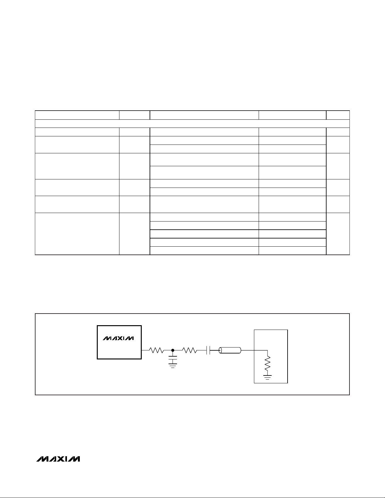
Note 4: Measured using setup shown in Figure 1 with V
CC
= 3.3V ±5%.
Note 5: Measured with Agilent DSO81304A 40GS/s real-time oscilloscope.
Note 6: Measured with 40mV
P-P
, 100kHz sinusoidal signal on the supply with V
CCA
connected as shown in Figure 2.
Figure 1. LVCMOS Output Measurement Setup
PARAMETER SYMBOL CONDITIONS MIN TYP MAX UNITS
CLOCK OUTPUT AC SPECIFICATIONS
VCO Frequency Range 620 625 648 MHz
Random Jitter RJ
Determin istic Jitter Induced by
Power-Supply Nois e
(Notes 5, 6)
Spurs Induced by Power-Supply
Noise (Note 6)
Nonharmonic and Subharmonic
Spurs
Clock Output SSB Phase Noise
at 125MHz
RMS
12kHz to 20MHz 0.36 1.0
1.875MHz to 20MHz 0.14
LVPECL o utput 4
LVCMOS output 19
LVPECL o utput -57
LVCMOS output -47
-70 dBc
f = 1kHz -124
f = 10kHz -126
f = 100kHz -130
f = 1MHz -145
f > 10MH z -153
ps
RMS
ps
P-P
dBc
dBc/Hz
MAX3622
QA_C
36Ω 499Ω
4.7pF
0.1μF
OSCILLOSCOPE
Z0 = 50Ω
50Ω
Page 4

MAX3622
Low-Jitter, Precision Clock Generator
with Two Outputs
4 _______________________________________________________________________________________
Typical Operating Characteristics
(Typical values are at VCC= +3.3V, TA= +25°C, crystal frequency = 25MHz.)
SUPPLY CURRENT vs. TEMPERATURE
MAX3622 toc01
AMBIENT TEMPERATURE (°C)
SUPPLY CURRENT (mA)
605040302010
25
50
75
100
125
150
0
070
BOTH OUTPUTS ACTIVE AND TERMINATEDBOTH OUTPUTS ACTIVE AND TERMINATED
BOTH OUTPUTS ACTIVE AND UNTERMINATED
BOTH OUTPUTS ACTIVE AND UNTERMINATED
DIFFERENTIAL OUTPUT WAVEFORM
AT 156.25MHz (LVPECL OUTPUT)
MAX3622 toc02
1ns/div
AMPLITUDE (200mv/div)
OUTPUT WAVEFORM AT 125MHz
(LVCMOS OUTPUT)
MAX3622 toc03
1ns/div
AMPLITUDE (50mV/div)
MEASURED USING 50Ω OSCILLOSCOPE INPUT
THROUGH NETWORK SHOWN IN FIGURE 1
QB PHASE NOISE
(156.25MHz CLOCK FREQUENCY)
MAX3622 toc04
OFFSET FREQUENCY (kHz)
NOISE POWER DENSITY (dBc/Hz)
10,00010001 10 100
-150
-140
-130
-120
-110
-100
-90
-80
-160
0.1 100,000
QA_C PHASE NOISE
(125MHz CLOCK FREQUENCY)
MAX3622 toc05
OFFSET FREQUENCY (kHz)
NOISE POWER DENSITY (dBc/Hz)
10,00010001 10 100
-150
-140
-130
-120
-110
-100
-90
-80
-160
0.1 100,000
Page 5
MAX3622
Pin Description
Low-Jitter, Precision Clock Generator
with Two Outputs
_______________________________________________________________________________________ 5
Detailed Description
The MAX3622 is a low-jitter clock generator designed
to operate at Ethernet frequencies. It consists of an onchip crystal oscillator, PLL, LVCMOS output buffer, and
an LVPECL output buffer. Using a 25MHz crystal as a
reference, the internal PLL generates a high-frequency
output clock with excellent jitter performance.
Crystal Oscillator
An integrated oscillator provides the low-frequency reference clock for the PLL. This oscillator requires a
25MHz crystal connected between X_IN and X_OUT.
PLL
The PLL takes the signal from the crystal oscillator and
synthesizes a low-jitter, high-frequency clock. The PLL
contains a phase-frequency detector (PFD), a lowpass
filter, and a voltage-controlled oscillator (VCO). The
VCO output is connected to the PFD input through a
feedback divider. The PFD compares the reference frequency to the divided-down VCO output (f
VCO
/25) and
generates a control signal that keeps the VCO locked
to the reference clock. The high-frequency VCO output
clock is sent to the output dividers. To minimize noiseinduced jitter, the VCO supply (V
CCA
) is isolated from
the core logic and output buffer supplies.
Output Dividers
The output dividers are set to divide-by-five for the
LVCMOS output QA_C and divide-by-four for the
LVPECL output QB.
LVPECL Driver
The differential PECL buffer (QB) is designed to drive
transmission lines terminated with 50Ω to VCC- 2.0V.
The output goes to a logic 0 when disabled.
LVCMOS Driver
QA_C, the LVCMOS output, is designed to drive a single-ended high-impedance load. This output goes to a
high-impedance state when disabled.
Reset Logic/POR
During power-on, the power-on reset (POR) signal is
generated to synchronize all dividers.
PIN NAME FUNCTION
1 QAC_OE
2 GNDO_A Ground for QA_C Output. Connect to supply ground.
3 QA_C LVCMOS Clock Output
4 V
5, 6 RES1, RES2 Reserved. Do not connect.
7 V
8 VCC Core Power Supply. Connect to +3.3V.
9, 15 GND Supply Ground
10 X_OUT Crysta l Oscillator Output
11 X_IN Crystal Oscillator Input
12 V
13 QB LVPECL, In verting Clock Output
14 QB LVPECL, Noninvert ing Cloc k Output
16 QB_OE
DDO_ A
CCA
CCO_ B
LVCMOS/LVTTL Input. Enables/disables QA_C clock output. Connect pin high to enable QA_C.
Connect low to set QA_C to a high-impedance state. Has internal 50k input impedance.
Power Supply for QA_C Clock Output. Connect to +3.3V.
Analog Power Supply for the VCO. Connect to +3.3V. For additional power-supply noi se fi lter ing,
this pin can connect to V
Power Supply for QB Clock Output. Connect to +3.3V.
LVCMOS/LVTTL Input. Enables/disables QB clock output. Connect pin high to enable LVPECL clock
output QB. Connect low to set QB to a logic 0. Has internal 50k input impedance.
through 10.5 as shown in Figure 2 (requires VCC = +3.3V ±5%).
CC
Page 6

Applications Information
Power-Supply Filtering
The MAX3622 is a mixed analog/digital IC. The PLL
contains analog circuitry susceptible to random noise.
In addition to excellent on-chip power-supply noise
rejection, the MAX3622 provides a separate powersupply pin, V
CCA
, for the VCO circuitry. Figure 2 illustrates the recommended power-supply filter network for
V
CCA
. The purpose of this design technique is to
ensure clean input power supply to the VCO circuitry
and to improve the overall immunity to power-supply
noise. This network requires that the power supply is
+3.3V ±5%. Decoupling capacitors should be used on
all other supply pins for best performance.
Crystal Selection
The crystal oscillator is designed to drive a fundamental mode, AT-cut crystal resonator. See Table 1 for recommended crystal specifications. See Figure 4 for
external capacitor connection.
Crystal Input Layout and Frequency
Stability
The crystal, trace, and two external capacitors should
be placed on the board as close as possible to the
MAX3622’s X_IN and X_OUT pins to reduce crosstalk
of active signals into the oscillator.
The layout shown in Figure 3 gives approximately 3pF
of trace plus footprint capacitance per side of the crystal (Y1). The dielectric material is FR-4 and dielectric
thickness of the reference board is 15 mils. Using a
25MHz crystal and the capacitor values of C10 = 27pF
and C9 = 33pF, the measured output frequency accuracy is -10ppm at +25°C ambient temperature.
Table 1. Crystal Selection Parameters
MAX3622
Low-Jitter, Precision Clock Generator
with Two Outputs
6 _______________________________________________________________________________________
Figure 2. Analog Supply Filtering
Figure 3. Crystal Layout
V
CC
V
CCA
MAX3622
10.5Ω
+3.3V ±5%
0.01μF
0.01μF 10μF
C 9
CRYSTAL
C 10
Y1
25MHz
PARAMETER S YMBOL MIN TYP MAX UNITS
Crystal Osci llation Frequency f
Shunt Capacitance CO 2.0 7.0 pF
Load Capacitance CL 18 pF
Equivalent Series Resistance
(ESR)
Max imum Crystal Drive Level 300 μW
25 MHz
OSC
R
50
S
Page 7
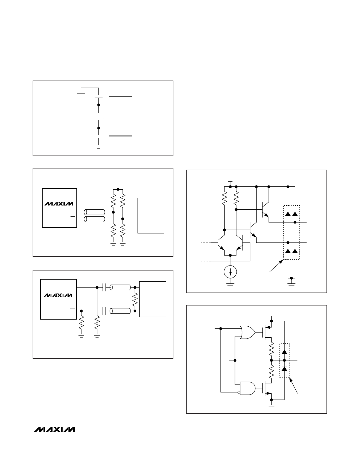
Interfacing with LVPECL Outputs
The equivalent LVPECL output circuit is given in Figure
7. This output is designed to drive a pair of 50Ω transmission lines terminated with 50Ω to VTT= VCC- 2V. If
a separate termination voltage (V
TT
) is not available,
other termination methods can be used such as shown
in Figures 5 and 6. Unused outputs should be disabled
and may be left open. For more information on LVPECL
terminations and how to interface with other logic families, refer to Maxim Application Note
HFAN-01.0:
Introduction to LVDS, PECL, and CML
.
Interface Models
Figure 7 and Figure 8 show examples of interface models.
MAX3622
Figure 4. Crystal, Capacitors Connection
Low-Jitter, Precision Clock Generator
with Two Outputs
_______________________________________________________________________________________ 7
Figure 5. Thevenin Equivalent of Standard PECL Termination
Figure 6. AC-Coupled PECL Termination
Figure 7. Simplified LVPECL Output Circuit Schematic
Figure 8. Simplified LVCMOS Output Circuit Schematic
27pF
X_IN
25MHz
CRYSTAL
= 18pF)
(C
L
X_OUT
33pF
+3.3V
130Ω 130Ω
MAX3622
QB
QB
Z
= 50Ω
0
Z0 = 50Ω
82Ω
82Ω
HIGH
IMPEDANCE
V
CC
QB
QB
0.1μF
0.1μF
150Ω
Z0 = 50Ω
100Ω
Z0 = 50Ω
HIGH
IMPEDANCE
QB
MAX3622
QB
150Ω
NOTE: AC-COUPLING IS OPTIONAL.
ESD
STRUCTURES
V
DDO_A
DISABLE
10Ω
IN
10Ω
GNDO_A
QA_C
ESD
STRUCTURES
Page 8

Layout Considerations
The inputs and outputs are critical paths for the
MAX3622, and care should be taken to minimize discontinuities on these transmission lines. Here are some
suggestions for maximizing the MAX3622’s performance:
• An uninterrupted ground plane should be positioned beneath the clock I/Os.
• Supply and ground pin vias should be placed
close to the IC and the input/output interfaces to
allow a return current path to the MAX3622 and the
receive devices.
• Supply decoupling capacitors should be placed
close to the MAX3622 supply pins.
• Maintain 100Ω differential (or 50Ω single-ended)
transmission line impedance out of the MAX3622.
• Use good high-frequency layout techniques and a
multilayer board with an uninterrupted ground
plane to minimize EMI and crosstalk.
Refer to the MAX3622 Evaluation Kit for more information.
MAX3622
Low-Jitter, Precision Clock Generator
with Two Outputs
8 _______________________________________________________________________________________
Typical Application Circuit
10μF
10.5Ω
0.01μF
V
CC
V
CCA
0.1μF
V
CCO_B
V
CC
+3.3V ±5%
125MHz
0.01μF 0.1μF
36Ω
Z0 = 50Ω
ASIC
0.1μF
V
DDO_A
QA_C
V
CC
QAC_OE
QB_OE
X_OUT
25MHz
= 18pF)
(C
L
33pF 27pF
MAX3622
X_IN GNDO_AGND
QB
QB
156.25MHz
= 50Ω
Z
0
Z0 = 50Ω
50Ω
50Ω
(V
ASIC
CC
- 2V)
Page 9
MAX3622
Low-Jitter, Precision Clock Generator
with Two Outputs
Maxim cannot assume responsibility for use of any circuitry other than circuitry entirely embodied in a Maxim product. No circuit patent licenses are
implied. Maxim reserves the right to change the circuitry and specifications without notice at any time.
Maxim Integrated Products, 120 San Gabriel Drive, Sunnyvale, CA 94086 408-737-7600 _____________________
9
© 2007 Maxim Integrated Products is a registered trademark of Maxim Integrated Products, Inc.
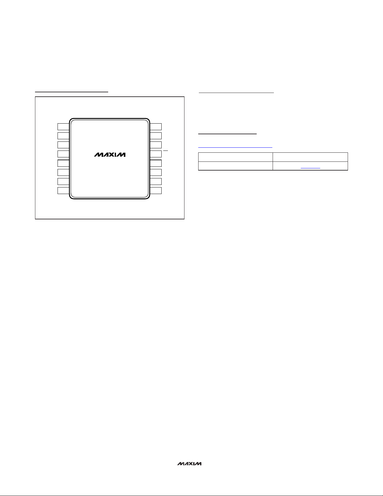
Pin Configuration
Chip Information
TRANSISTOR COUNT: 10,490
PROCESS: BiCMOS
Package Information
For the latest package outline information, go to
www.maxim-ic.com/packages
.
PACKAGE TYPE DOCUMENT NO.
16 TSSOP
21-0066
TOP VIEW
GNDO_A
V
DDO_A
CCA
+
2
4
5RES1
CC
MAX3622
TSSOP
16 QB_OE1QAC_OE
15 GND
14 QB3QA_C
QB
13
12 V
11 X_IN6RES2
10 X_OUT7V
9 GND8V
CCO_B
 Loading...