

Page 1
General Description
The MAX3580 fully integrated, direct-conversion TV tuner
is designed for Digital Video Broadcasting-Terrestrial
(DVB-T) applications. The integrated tuner covers a
170MHz to 230MHz input frequency range for the VHF-III
band and 470MHz to 878MHz for the UHF band.
The MAX3580 direct-conversion tuner integrates an RF
input switch and a multiband tracking filter, allowing
low-power tuner-on-board applications without the cost
and power-dissipation issues of dual-conversion tuner
solutions. The zero-IF architecture eliminates the need
for SAW filters by providing baseband I and Q outputs
directly to the demodulator. In addition, DC-offset cancellation is implemented on-chip using a mixed-signal
architecture to improve the second-order distortion performance and the dynamic range of the downstream
digitizer and demodulator.
The MAX3580 features dynamic gain control of more
than 76dB and a typical midband noise figure of 4.7dB
referred to the LNA input. The VCO architecture optimizes both in-band and wideband phase noise for
OFDM applications where sensitivity to both 1kHz
phase noise and wideband phase noise related to
strong adjacents can be a problem.
The MAX3580 communicates using a 2-wire serial bus.
The device operates from a typical +3.3V power supply
and dissipates 650mW. The MAX3580 is available in a
small 32-pin thin QFN package (5mm x 5mm) with an
exposed paddle. Electrical performance is guaranteed
over the extended -40°C to +85°C temperature range.
Applications
Digital Televisions
Digital Terrestrial Set-Tops
Laptop Televisions
Automotive Televisions
USB Peripherals
Features
o 650mW Power Dissipation (at VCC= +3.3V)
o I and Q Baseband Outputs Eliminate All IF-SAW
Filters
o Integrated RF Tracking Filters
o Tunable Baseband Lowpass Filters
o Full-Band VHF-III and UHF Tuning
o +38dB Digital ACPR, +47dB Analog ACPR
o Low Noise Figure: 4.7dB (typ)
o Frac-N Synthesizer for -90dBc/Hz Close-In
Phase Noise
o Baseband Overload Detector Controls RF AGC if
Desired
o +3.1V to +3.5V Supply Voltage Range
o Ultra-Small, 5mm x 5mm Thin QFN Package
MAX3580
Direct-Conversion TV Tuner
________________________________________________________________
Maxim Integrated Products
1
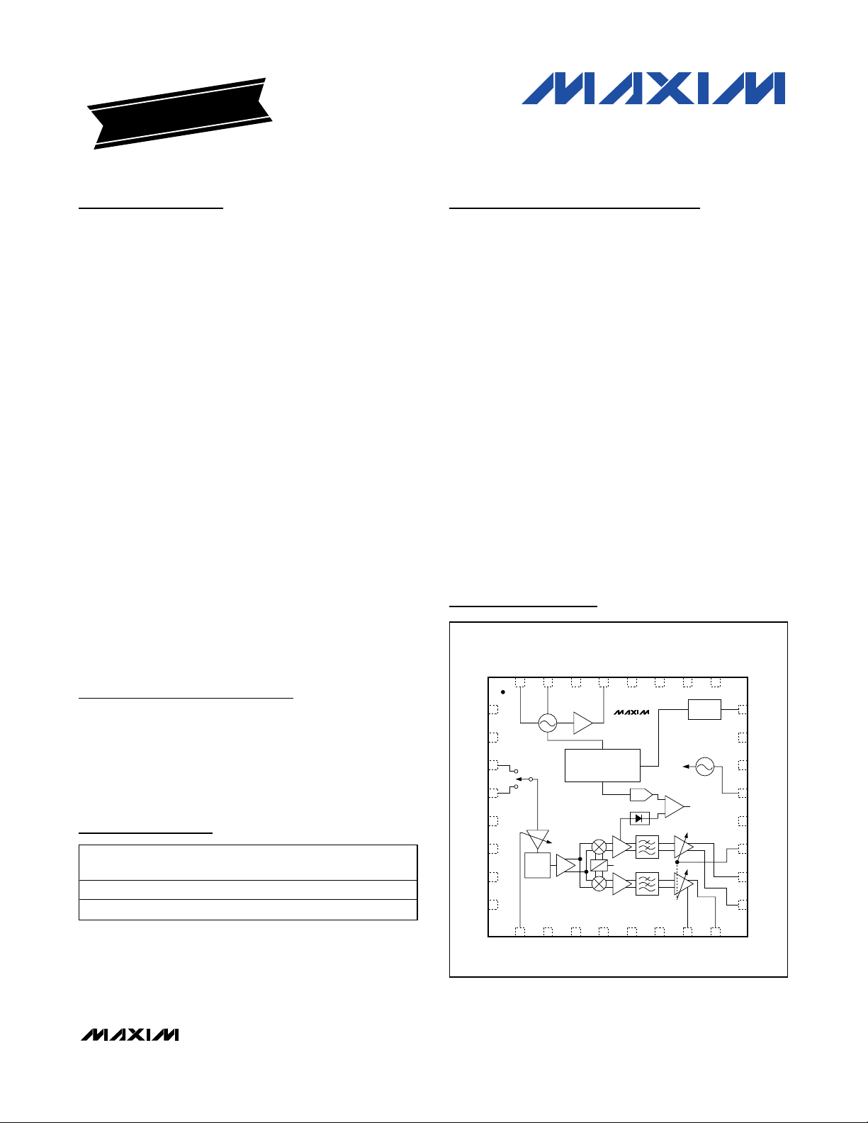
Pin Configuration/
Functional Diagram
Ordering Information
TRACKING
FILTER
GND_TUNE
LDO
XE
XB
VCC_VCO
MUX
RFIN2
ADDR2
LEXT
VCC_SYN
RFIN
RF_AGC
SCL
SDA
BBI-
BBQ-
BBQ+
BB_AGC
BBI+
VCC_BB
REF_BUFF
VCC_RF
OVLD_DET
IND1
IND2
VCC_XTAL
VTUNE
CP
OVLD_DET
GND_LNA
GND_CP
GND_PLL
N.C.
TOP VIEW
32 28
293031
25
26
27
10
13
15
14
1611 12
9
17
18
19
20
21
22
23
24
2
3
4
5
6
7
8
1
MAX3580
0
90
DAC
LO
LO
CHARGE
PUMP
SERIAL INT ERFACE, CON TROL,
AND
SYNTHESIZER
19-0611; Rev 0; 7/06
For pricing, delivery, and ordering information, please contact Maxim/Dallas Direct! at
1-888-629-4642, or visit Maxim’s website at www.maxim-ic.com.
*
EP = Exposed paddle.
+
Denotes lead-free package.
T
= Tape-and-reel package.
EVALUATION KIT
AVAILABLE
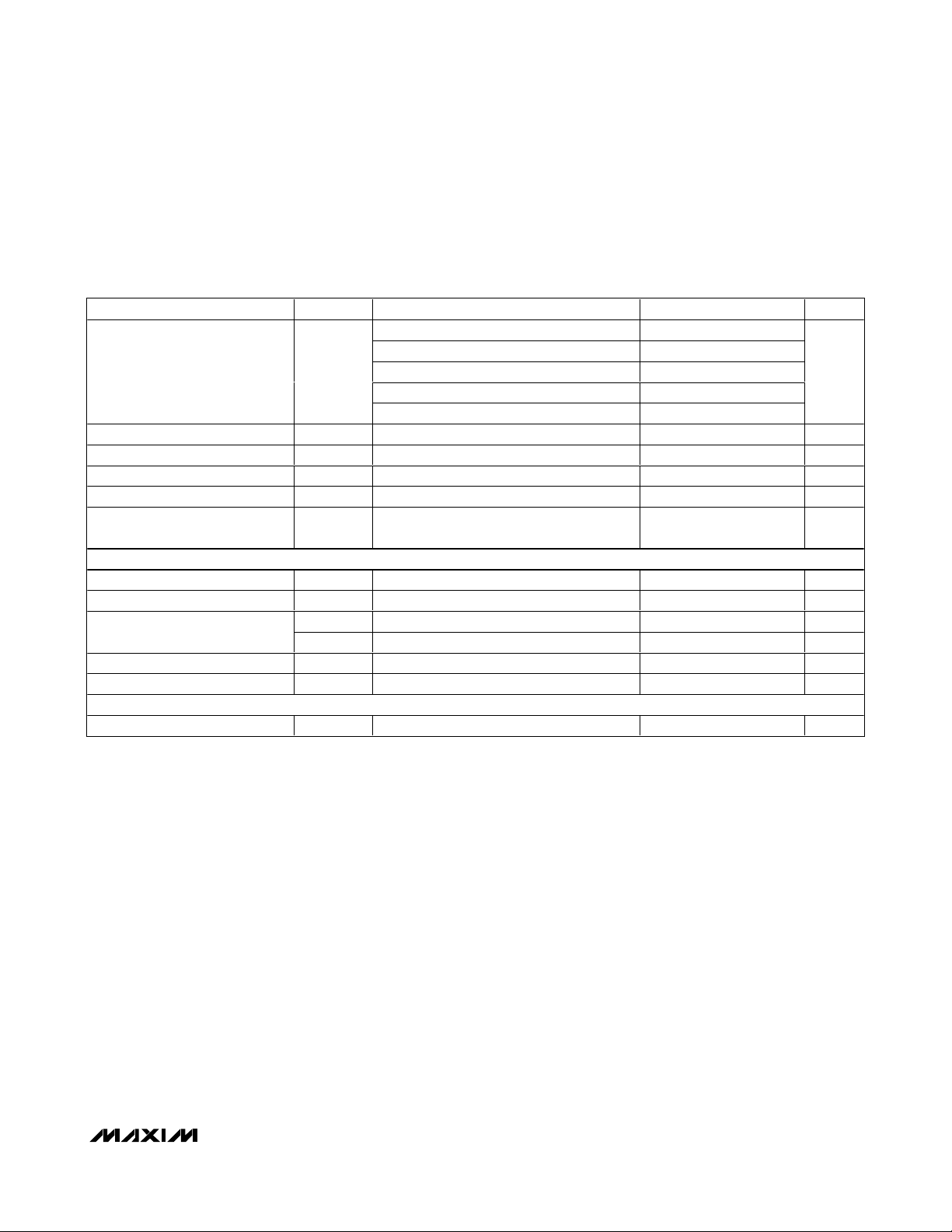
PART TEMP RANGE
MAX3580ETJ+ -40°C to +85°C 32 TQFN-EP* T3255-5
MAX3580ETJ+T -40°C to +85°C 32 TQFN-EP* T3255-5
PIN-
PACKAGE
PKG
CODE
Page 2
MAX3580
Direct-Conversion TV Tuner
2 _______________________________________________________________________________________
ABSOLUTE MAXIMUM RATINGS
DC ELECTRICAL CHARACTERISTICS
(MAX3580 EV kit, VCC= +3.1V to +3.5V, GND = 0V, BB_AGC = RF_AGC = +2.85V, RF input terminated into a 75Ω load, BBI_ and
BBQ_ are open, no input signal, VCO active, registers set according to the specified default register conditions, T
A
= -40°C to
+85°C, unless otherwise specified. Typical values are at V
CC
= +3.3V, TA=+25°C, unless otherwise specified.) (Note 1)
Stresses beyond those listed under “Absolute Maximum Ratings” may cause permanent damage to the device. These are stress ratings only, and functional
operation of the device at these or any other conditions beyond those indicated in the operational sections of the specifications is not implied. Exposure to
absolute maximum rating conditions for extended periods may affect device reliability.
VCCto GND...........................................................-0.3V to +3.6V
SDA, SCL, ADDR2, MUX, REF_BUFF,
BB_AGC, RF_AGC to GND ................................-0.3V to +3.6V
All Other Pins to GND ..............................-0.3V to (+V
CC
+ 0.3V)
RF Input Power ...............................................................+10dBm
Operating Temperature Range ...........................-40°C to +85°C
Junction Temperature......................................................+150°C
Storage Temperature Range .............................-65°C to +165°C
Continuous Power Dissipation (T
A
= +70°C)
(derate 21.3mW/°C above +70°C)..............................1702mW
Lead Temperature (soldering, 10s) .................................+300°C
CAUTION! ESD SENSITIVE DEVICE
SUPPLY VOLTAGE AND CURRENT
Supply Voltage V
Supply Current I
PARAMETER SYMBOL CONDITIONS MIN TYP MAX UNITS
CC
CC
Active 197 225 mA
Shutdown mode 200 µA
RF_AGC AND BB_AGC
Input Bias Current I
RF and Baseband AGC Control
Voltage
V
AGC
AGC
V
at +0.5V and +2.85V -50 +50 µA
AGC
Maximum gain 2.85
Minimum gain 0.5
SERIAL INTERFACE AND MUX OUTPUT (SCL, SDA, MUX)
Input Logic-Level Low V
Input Logic-Level High V
IL
IH
Input Hysteresis
SDA, SCL Input Current -10 +10 µA
Output Logic-Level Low V
Output Logic-Level High V
OL
OH
Sink current = 0.3mA 0.4 V
Source current = 0.3mA
3.1 3.5 V
0.3 x
0.7 x
V
CC
0.05 x
V
V
-
CC
0.5
V
V
CC
V
CC
V
V
V
Page 3
MAX3580
Direct-Conversion TV Tuner
_______________________________________________________________________________________ 3
AC ELECTRICAL CHARACTERISTICS
(MAX3580 EV kit, VCC= +3.1V to +3.5V, GND = 0V. RF_AGC = BB_AGC = +2.85V, RF input terminated into a 75Ω load, BBI_ and
BBQ_ loaded by R
L
greater than 2kΩ and CLless than 10pF, VCO active, registers are set according to the recommended default
register conditions, T
A
= -40°C to +85°C, unless otherwise noted. Typical values are at VCC= +3.3V, TA= +25°C, unless otherwise
noted.) (Note 1)
PARAMETER SYMBOL CONDITIONS MIN TYP MAX UNITS
Operating Frequency Range f
Overall Voltage Gain (Note 2)
RF Gain Flatness W i thi n each V H F- III and U H F b and ( N ote 10) -3 +3 dB
RF
Gain specification met across this
frequency band
RF_AGC = BB_AGC = +2.85V 74
RF_AGC = BB_AGC = +0.5V 26
170 230
470 878
MHz
dB
Input Return Loss Wor st case acr oss b and sel ected , 75Ω system 7 dB
230MHz 5.4
Noise Figure (DSB) (Notes 3, 4) NF
470MHz 4.7
dB
858MHz 6.5
Input 2nd-Order Intercept Point IIP2
Broadband (Notes 4, 5) 12
Br oad b and , RF_AGC ad j usted for 49d B of g ai n > 26
dBm
Broadband (Notes 4, 6) > -4
Br oad b and , RF_AGC ad j usted for 49d B of g ai n > 12
RF 1dB Desense
LO Harmonic Reception
RF Channel Flatness
Isolation
Quadrature Accuracy
Narrowband (Notes 4, 7) -15 Input 3rd-Order Intercept Point IIP3
Narrowband, RF_AGC adjusted for 49dB of
gain (Note 7)
P
DESIRED
3.75MHz, P
RF_AGC adjusted for 49dB of gain,
P
DESIRED
= -78dBm and converted to
10MHz higher (Note 4)
TONE
= -55dBm
3
-24
-1
RF i np ut r ang e of 170M H z to 960M H z ( N ote 8) -60
RF input range of 960MHz to 1400MHz > -40
8MHz RF channel at baseband, tested at
169MHz and 469MHz
DC to 30MHz, RF input to baseband output,
relative to desired channel
-1 +1 dB
> 60 dBc
I/Q phase error at 1MHz -3 +3 D eg r ees
I/Q amplitude error at 1MHz -1.5 +1.5 dB
dBm
dBm
dBc
50MHz to 470MHz -50 -20
Spurious at the RF Input (Note 3)
470MHz to 878MHz -50 -35
878MHz to 1732MHz < -50 -20
dBmV
At 1kHz to 10kHz (Note 3) -80 -90
Phase Noise (Single-Sideband,
Closed Loop)
ΦN
At 100kHz (Note 3) -94 -107
dBc/Hz
At 1MHz -130
Page 4
MAX3580
Direct-Conversion TV Tuner
4 _______________________________________________________________________________________
AC ELECTRICAL CHARACTERISTICS (continued)
(MAX3580 EV kit, VCC= +3.1V to +3.5V, GND = 0V. RF_AGC = BB_AGC = +2.85V, RF input terminated into a 75Ω load, BBI_ and
BBQ_ loaded by R
L
greater than 2kΩ and CLless than 10pF, VCO active, registers are set according to the recommended default
register conditions, T
A
= -40°C to +85°C, unless otherwise noted. Typical values are at VCC= +3.3V, TA= +25°C, unless otherwise
noted.) (Note 1)
PARAMETER SYMBOL CONDITIONS MIN TYP MAX UNITS
SIGMA-DELTA FRACTIONAL-N SYNTHESIZER
REFERENCE OSCILLATOR
Frequency f
Input Impedance Z
Voltage Gain 30 V/V
Output Impedance Z
Buffered Output 10kΩ || 10pF load 0.7 V
DIVIDERS
RF N Divider Ratio 5 251 —
RF R Divider Ratio 1 2 —
Fractional-N Resolution 20 Bits
LO PHASE DETECTOR AND CHARGE PUMP
Phase-Detector Frequency 4 27 MHz
Charge-Pump Current I
Charge-Pump Tri-State Current -10 +10 µA
Charge-Pump Compliance
Range
LOCAL OSCILLATOR
Tuning Frequency Range f
VCO Dividers 4 16 —
BASEBAND STAGE
Nominal Output Voltage (Note 2) 1 V
1dB Output Compression Point P
Output Impedance Differential 60 Ω
Passband AGC Range BB_AGC = 0.5V to 2.85V 30 50 dB
Passband Cutoff Attenuation
Passband Differential Gain Error
Passband Group Delay
Group Delay Mismatch
REF
IN
OUT
CP
OSC
1dB
Gain = 0 600
Gain = 1 1200
Charge-pump positive to negative current
matching of ≤ ±5%
Tank Frequency 2160 4400 MHz
Differential voltage at 3MHz 1.6 2 V
At 3.8MHz (UHF Mode);
at 3.325MHz (VHF Mode)
2MHz to 3.8MHz, I channel vs. Q channel
(UHF mode)
From DC to 3.8MHz over any 1.1kHz band
(UHF mode)
From 0.1MHz to 3.8MHz, I channel vs. Q
channel (UHF mode) (Note 9)
4 27 MHz
10 kΩ
15 Ω
VCC -
0.4
0.4
2 5 dB
-0.45 +0.45 dB
5 ns
< 2 ns
µA
P-P
V
P-P
P-P
Page 5
MAX3580
Direct-Conversion TV Tuner
_______________________________________________________________________________________ 5
AC ELECTRICAL CHARACTERISTICS (continued)
(MAX3580 EV kit, VCC= +3.1V to +3.5V, GND = 0V. RF_AGC = BB_AGC = +2.85V, RF input terminated into a 75Ω load, BBI_ and
BBQ_ loaded by R
L
greater than 2kΩ and CLless than 10pF, VCO active, registers are set according to the recommended default
register conditions, T
A
= -40°C to +85°C, unless otherwise noted. Typical values are at VCC= +3.3V, TA= +25°C, unless otherwise
noted.) (Note 1)
Note 1: Min and Max limits are guaranteed by test above TA= +25°C and are guaranteed by design and characterization at
T
A
= -40°C. The default register settings are not production tested. Load registers no sooner than 100µs after power-up.
Note 2: The specified overall voltage gain is suitable to amplify -93dBm to -20dBm to 1V
P-P
at the baseband output.
Note 3: Guaranteed by design characterization over the specified operating conditions. Not production tested.
Note 4: BB_AGC adjusted for gain = 72dB with RF_AGC at 2.85V.
Note 5: Two tones at a) 230MHz and 431MHz with IM measured at 201MHz and b) 230MHz and 701MHz with IM measured at
471MHz.
Note 6: Two tones at 499MHz and 689MHz with IM measured at 879MHz.
Note 7: IM3 measured with two tones within the adjacent channel. Production tested at 72dB of gain with two tones at a)
205.75MHz and 210.5MHz with IM measured at 201MHz and b) 475.25MHz and 479.5MHz with IM measured at
471MHz. Production tested at 49dB of gain with two tones at 475.25MHz and 479.5MHz with IM measured at 471MHz.
Note 8: Measured at RF = 171MHz with harmonics at 511MHz (3rd harmonic) and 851MHz (5th harmonic).
Note 9: Delay of 2ns equal 2.74° phase error.
Note 10: UHF rolloff of 4dB in addition to gain flatness specification.
Note 11: Production tested at V
CC
= +3.5V to limits of 1.7V ±0.1V.
Rejection Ratio
DC Output Voltage V
Output DC Offset BB_AGC = 2.85V -70 +70 mV
Baseband Highpass Cutoff Programmable 20 to 200 Hz
AGC Gain Slope BB_AGC = 0.5V to 2.85V 14 35 dB/V
PARAMETER SYMBOL CONDITIONS MIN TYP MAX UNITS
Ratio of Passband to Stopband
Noise
At 5.25MHz (UHF mode) 23
At 4.75MHz (VHF mode) 23
At 13.25MHz (UHF mode) 63
At 11.75MHz (VHF mode) 62
At > 16.2MHz
CM
Common mode (Note 11) 0.485 x V
BB_AGC = 2.85V, 10kHz to 3.8MHz vs.
16.2MHz to 23.8MHz
84
V
CC
15 dB
dB
DC
MIXER OVERLOAD DETECTOR (RSSI)
Attack-Point Accuracy 5.25MHz test tone ±1 dB
Attack-Point Increment 3-bit DAC 1.5 dB
Detector Output Sink
Detector on, V
Detector off, V
= 0.5V 0.3 mA
OUT
= 2.85V 5 µA
OUT
Detector Gain 30 V/V
Detector Response Time < 200 µs
2-WIRE INTERFACE
Clock Rate 400 kHz
Page 6
MAX3580
Direct-Conversion TV Tuner
6 _______________________________________________________________________________________
Performance to Standards
The following is selected overall performance data for the
MAX3580 + digital demodulator.
Table 1 shows the typical overall performance as measured using the MAX3580 and one current production
DVB-T demodulator. This reference design is available
in NIM card form factor upon request.
MBRAI refers to standard MBRAI 04-102 IEC 62002-1
available from www.ansi.org.
NorDig refers to standard Unified 1.0.2 available from
www.nordig.org.
Modulation of wanted and interfering channel(s) is 8k
mode, 16 QAM, C/R = 3/4, GI = 1/4, sensitivity or
immunity Reference Bit Error Rate is 2 x 10e-4, unless
stated otherwise.
Table 1. Selected Typical MBRAI and NorDig Performance
TEST SCENARIO COMMENTS SPEC MINIMUM MAX3580 TYPICAL
MBRAI S2 Immunity/ACPR for N ±1 adjacent ch. 29dB 40dB
MBRAI S2 Immunity/ACPR N ±2 alternate ch. 40dB 43dB
MBRAI L3 Li near ity/c r ossm od . w i th N +2 and N +4 ch. 40dB 47dB
NorDig 16 QAM 2/3 S ensi ti vi ty at channel 21 ( 470 M H z) -84.1dBm -85.1dBm
NorDig QPSK 1/2 Sensitivity at channel 42 (642 MHz) -92.1dBm -94.8dBm
NorDig 64 QAM 7/8 Sensitivity at channel 59 (778 MHz) -74.7dBm -76dBm
Page 7
MAX3580
Direct-Conversion TV Tuner
_______________________________________________________________________________________
7
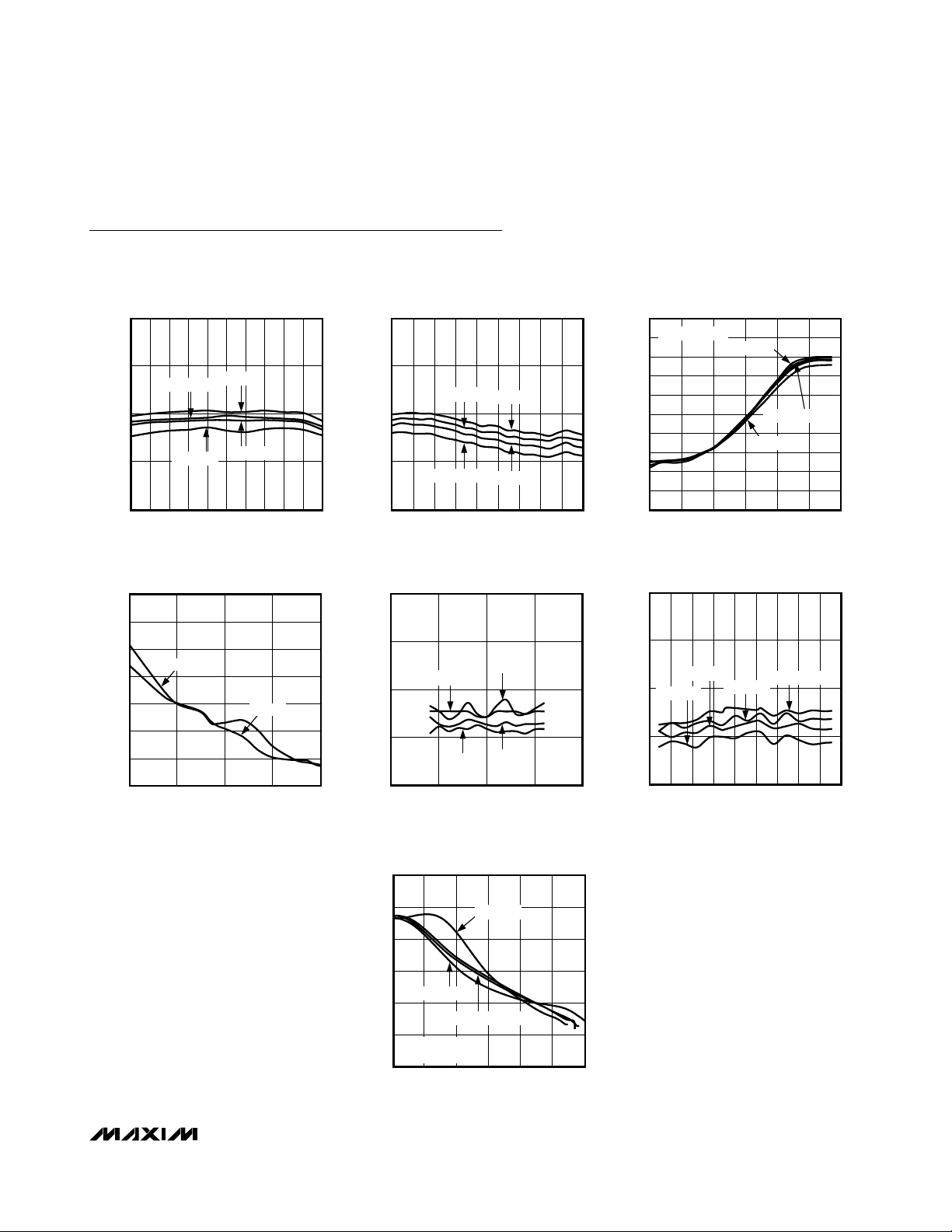
Typical Operating Characteristics
(Typical values are at VCC= +3.3V, TA= +25°C, unless otherwise noted.)
0
10
5
20
15
25
30
VHF MODE NOISE FIGURE
vs. VOLTAGE GAIN
MAX3580 toc07
VOLTAGE GAIN (dB)
NOISE FIGURE (dB)
60 70 7565 80 85 90
TA = +25°C, +55°C
TA = -40°C
TA = +85°C
fRF = 220MHz
BB_AGC = 2.85V
VHF-III BAND VOLTAGE GAIN
vs. FREQUENCY
110
100
TA = +25°C
90
GAIN (dB)
80
70
150 170 180 190 200160 210 220 230 240 250
TA = +85°C
TA = 0°C
TA = +55°C
FREQUENCY (MHz)
PHASE NOISE vs. OFFSET FREQUENCY
-50
-60
-70
-80
-90
PHASE NOISE (dBm/Hz)
-100
-110
-120
620MHz
220MHz
0.1 1 10 100 1000
OFFSET FREQUENCY (kHz)
MAX3580 toc01
MAX3580 toc04
110
100
90
GAIN (dB)
80
70
20
15
10
NOISE FIGURE (dB)
UHF BAND VOLTAGE GAIN
vs. FREQUENCY
TA = +25°C
TA = +85°C
450 550 600 650 700500 750 800 850 900
TA = +55°C
FREQUENCY (MHz)
NOISE FIGURE vs. VHF FREQUENCY
TA = +55°C
5
TA = -40°C
0
150 175 200 225 250
TA = +85°C
TA = +25°C
FREQUENCY (MHz)
TA = 0°C
MAX3580 toc02
MAX3580 toc05
VOLTAGE GAIN
vs. RF_AGC CONTROL VOLTAGE
110
BB_AGC = 2.85V
100
90
80
70
60
GAIN (dB)
50
40
30
20
10
01.00.5 1.5 2.0 2.5 3.0
RF_AGC CONTROL VOLTAGE (V)
TA = -40°C
TA = +25°C, +55°C
TA = +85°C
NOISE FIGURE vs. UHF FREQUENCY
20
15
TA = +25°C
10
TA = -40°C
NOISE FIGURE (dB)
5
0
450 550 600 650 700500 750 800 850 900
TA = +55°C
FREQUENCY (MHz)
TA = +85°C
MAX3580 toc03
MAX3580 toc06
Page 8

MAX3580
Direct-Conversion TV Tuner
8 _______________________________________________________________________________________
Typical Operating Characteristics (continued)
(Typical values are at VCC= +3.3V, TA= +25°C, unless otherwise noted.)
UHF MODE NOISE FIGURE
vs. VOLTAGE GAIN
30
25
20
TA = +25°C
15
NOISE FIGURE (dB)
10
5
fRF = 620MHz
BB_AGC = 2.85V
0
60 70 7565 80 85 90
TA = +85°C
TA = -40°C
VOLTAGE GAIN (dB)
NORMALIZED BASEBAND FREQUENCY
RESPONSE
5
0
-5
TA = 0°C
-10
-15
-20
-25
GAIN (dB)
-30
-35
-40
BB_BW<3:0> = "1011"
-45
8MHz CHANNEL MODE
-50
021345
TA = +25°C
FREQUENCY (MHz)
TA = +55°C
TA = +85°C
MAX3580 toc08
MAX3580 toc11
VOLTAGE GAIN
vs. BB_AGC CONTROL VOLTAGE
110
RF_AGC = 2.85V
100
90
80
70
60
GAIN (dB)
50
40
30
20
10
01.00.5 1.5 2.0 2.5 3.0
TA = -40°C
TA = +25°C, +55°C
TA = +85°C
BB_AGC CONTROL VOLTAGE (V)
MAX3580 toc09
NORMALIZED BASEBAND FREQUENCY
RESPONSE
5
0
-5
TA = 0°C
-10
-15
-20
-25
GAIN (dB)
-30
-35
-40
-45
-50
021345
TA = +25°C
BB_BW<3:0> = "1001"
7MHz CHANNEL MODE
FREQUENCY (MHz)
TA = +85°C
MAX3580 toc12
BASEBAND FILTER REJECTION RATIO
0
-10
-20
-30
-40
-50
-60
-70
REJECTION RATIO (dB)
-80
-90
-100
0 5 10 15 20
VHF INPUT
NOISE LIMITED
FREQUENCY (MHz)
UHF INPUT
NORMALIZED BASEBAND FREQUENCY
RESPONSE
5
0
-5
-10
-15
-20
-25
GAIN (dB)
-30
-35
-40
-45
-50
0105152025
BB_BW<3:0> = "1011"
8MHz CHANNEL MODE
TA = +85°C
TA = 0°C
TA = +25°C
FREQUENCY (Hz)
MAX3580 toc10
MAX3580 toc13
NORMALIZED BASEBAND FREQUENCY
RESPONSE
5
0
-5
-10
-15
-20
GAIN (dB)
-25
-30
-35
-40
-45
0 5 10 15 20 25
BB_BW <3:0> = "1001"
7MHz CHANNEL MODE
TA = +85°C
TA = 0°C
FREQUENCY (MHz)
MAX3580 toc14
TA = +25°C
Page 9

MAX3580
Direct-Conversion TV Tuner
_______________________________________________________________________________________
9
Typical Operating Characteristics (continued)
(Typical values are at VCC= +3.3V, TA= +25°C, unless otherwise noted.)
0
-5
-10
-15
-20
150 200175 225 250
RF INPUT RETURN LOSS
vs. VHF FREQUENCY
MAX3580 toc21
VHF FREQUENCY (MHz)
RETURN LOSS (dB)
Zo = 75Ω
200
195
190
185
3.0 3.33.1 3.2 3.4 3.5 3.6
SUPPLY CURRENT
vs. SUPPLY VOLTAGE
MAX3580 toc22
VCC (V)
I
CC
(mA)
TA = +55°C
TA = +85°C
TA = -40°C
TA = 0°C
TA = +25°C
STOPBAND NOISE vs. FREQUENCY
-45
-55
STOPBAND NOISE (dBm)
-65
-75
02010 30 40 50
BB_BW <3:0> = "1011"
8MHz CHANNEL MODE
BB_BW <3:0> = "1001"
7MHz CHANNEL MODE
FREQUENCY (MHz)
RF PORT-TO-PORT ISOLATION
40
35
30
25
20
GAIN (dB)
15
RFIN TO RFIN2
10
5
0
100 300 400 500 600200 700 800 900 1000
RFIN2 TO RFIN
FREQUENCY (MHz)
30
25
MAX3580 tpc15
20
15
NOISE FIGURE (dB)
10
MAX3580 toc18
POWER-DETECTOR OUTPUT VOLTAGE (V)
VHF MODE NOISE FIGURE
vs. BB_AGC VOLTAGE
TA = +55°C
TA = +85°C
5
TA = -40°C
0
0 1.0 1.50.5 2.0 2.5 3.0
TA = +25°C
BB_AGC VOLTAGE (V)
POWER-DETECTOR OUTPUT VOLTAGE
vs. RF INPUT POWER
4
10kΩ PULLUP TO 3.0V
3
"000"
2
1
0
-60 -30-50 -40 -20 -10 0
RF INPUT POWER (dBm)
220MHz
RF_AGC = 2.85V
"111"
MAX3580 toc16
MAX3580 tpc19
UHF MODE NOISE FIGURE
vs. BB_AGC VOLTAGE
30
25
20
15
NOISE FIGURE (dB)
10
5
TA = -40°C
0
0 1.0 1.50.5 2.0 2.5 3.0
TA = +55°C
BB_AGC VOLTAGE (V)
620MHz
RF_AGC = 2.85V
TA = +85°C
TA = +25°C
RF INPUT RETURN LOSS
vs. UHF FREQUENCY
0
Zo = 75Ω
-5
RETURN LOSS (dB)
-10
-15
450 675525 600 750 825 900
UHF FREQUENCY (MHz)
MAX3580 toc17
MAX3580 toc20
Page 10

MAX3580
Direct-Conversion TV Tuner
10 ______________________________________________________________________________________
Pin Description
PIN NAME FUNCTION
1 SDA Serial-Data Input Line. Requires a pullup resistor to VCC.
2 SCL Serial-Clock Input. Requires a pullup resistor to VCC.
3 RFIN2 Second RF Input
4 RFIN First RF Input
5 ADDR2
6 GND_LNA Not Internally Connected. Connect to ground.
7 VCC_RF DC Supply for RF LNA. Connect as close as possible a 100pF capacitor from this pin to GND.
8 LEXT External Bias Inductor. Connect to VCC with a 270nH inductor.
9 RF_AGC Gain Control Input for RF VGA.
10 IND1 VHF Inductor Pin 1. Keep traces to inductor as short as possible.
11 IND2 VHF Inductor Pin 2. Keep traces to inductor as short as possible.
12 N.C. No Connection
13 OVLD_DET Overload Detector Output. Connect a 10kΩ pullup resistor to VCC and a RC network to RF_AGC.
14 VCC_BB D C S up p l y for Baseb and Fi l ter . C onnect as cl ose as p ossi b l e a 10nF cap aci tor fr om thi s p i n to g r ound .
15 BBQ- Quadrature Inverted Baseband Output
16 BBQ+ Quadrature Noninverted Baseband Output
17 BBI- In-Phase, Inverted Baseband Output
18 BBI+ In-Phase, Noninverted Baseband Output
19 BB_AGC Gain Control Input for Baseband VGAs
20 VCC_VCO DC Supply for the VCO. Connect as close as possible a 100pF capacitor from this pin to ground.
21 VTUNE VCO Tuning Voltage Input. Connect the PLL loop filter output directly to this pin.
22 GND_TUNE Ground Reference for the Tuning Voltage. Connect to ground of the loop filter.
23 LDO VCO LDO Output. Connect a 0.1µF capacitor to ground.
24 CP Charge-Pump Output. Connect the charge-pump output to the PLL loop filter input.
25 GND_CP Ground for the Charge Pump
26 VCC_SYN
27 GND_PLL Ground for the PLL
28 MUX Multiplex Output Line. Can be used as a PLL lock-detector output.
29 REF_BUFF Buffered Output of Reference Oscillator
30 VCC_XTAL D C S up p l y for Refer ence Osci l l ator . C onnect as cl ose as p ossi b l e a 10nF cap aci tor fr om thi s p i n to g r ound .
31 XB
32 XE Reference Oscillator Feedback. Connect to a capacitive divider when used in self-oscillating mode.
EP EP Exposed Paddle. Solder to the board’s ground plane to achieve the lowest possible impedance path.
Address Line. Sets the 3rd LSB of the device address. Connect to ground to set for “0” or V
for “1.”
DC Supply for Synthesizer and Serial-Interface Control. Connect as close as possible a 10nF
capacitor from this pin to ground.
Reference Input. Connect to a parallel resonant mode XTAL through a load-matching capacitor, or
can also be used as a reference clock input pin.
to set
CC
Page 11

MAX3580
Direct-Conversion TV Tuner
______________________________________________________________________________________ 11
Typical Application Circuit
ADDR2
SDA
SCL
RFIN2
RFIN
V
XE
XB
VCC_XTAL
32 28
1
2
3
4
5
SERIAL I NTERF ACE, CONTROL,
CC
293031
AND
SYNTHESIZER
REF_BUFF
MUX
MAX3580
DAC
V
CC
VCC_SYN
26
OVLD_DET
CHARGE
PUMP
GND_CP
25
CP
24
LDO
23
GND_TUNE
22
VTUNE
21
20
VCC_VCO
V
CC
GND_PLL
27
LO
GND_LNA
6
TRACKING
VCC_RF
LEXT
7
8
V
CC
V
CC
FILTER
10
9
IND1
RF_AGC
IND2
0
LO
90
14
13
N.C.
OVLD_DET
15
BBQ-
VCC_BB
V
CC
19
BBI+
18
BBI-
17
1611 12
BBQ+
I CHANNEL
Q CHANNEL
OVLD_DET
BB_AGC
Page 12

MAX3580
Direct-Conversion TV Tuner
12 ______________________________________________________________________________________
Detailed Description
Programmable Registers
The MAX3580 includes thirteen write/read registers and
three read-only registers. See Table 2 for register configuration and the
Register Description
section. The
register configuration of Table 2 shows each bit name
and the bit usage information for all registers. “U”
labeled under each bit name indicates that the bit
value is user defined to meet specific application
requirements. A “0” or “1” indicates that the bit must be
set to the defined “0” or “1” value for proper operation.
Operation is not tested or guaranteed if these bits are
programmed to other values and is only for
factory/bench evaluation. For field use, always program
to the defined operational state. Note that all registers
must be written after and no earlier than 100µs after
device power-up.
Table 2. Register Configuration
REGISTER
ADDRESS
0x00
0x01
0x02
0x03
0x04
0x05
0x06
0x07
0x08
0x09
0x0A
0x0B
0x0C
0x0D
0x0E
0x0F
0x10 TFR<7> TFR<6> TFR<5> TFR<4> TFR<3> TFR<2> TFR<1> TFR<0>
0x11 POR VASA VASE LD DC_LO DC_HI GKT PD_OVLD N/A N/A
0x12 VCO1A VCO0A BS2A BS1A BS0A ADC2 ADC1 ADC0 N/A N/A
TFS<7>UTFS<6>UTFS<5>UTFS<4>UTFS<3>UTFS<2>UTFS<1>UTFS<0>
VCO_DIV1UVCO_DIV0
RDIV
CP_TST20CP_TST10CP_TST0
VCO1
BB_BW3UBB_BW2UBB_BW1UBB_BW0
BB_BIA0DC_DAC80DC_MO11DC_MO01DC_SP11DC_SP00DC_TH10DC_TH0
DC_DAC70DC_DAC60DC_DAC50DC_DAC40DC_DAC30DC_DAC20DC_DAC10DC_DAC0
TFD<7>0TFD<6>0TFD<5>0TFD<4>0TFD<3>0TFD<2>0TFD<1>0TFD<0>
D7 D6 D5 D4 D3 D2 D1 D0
N7
U
MP
0
F15
U
F7
U
U
X
0
U
X
0
X
0
N6
U
LI1
0
F14
U
F6
U
U
ICP
U
SHDN_BGUSHDN_PDUSHDN_REFUSHDN_SYNUSHDN_MXUSHDN_BBUSHDN_RF
VCO0
U
FUSE_TH
0
X
0
N5
U
LI0
F13
U
F5
U
RFS
U
CPS
U
BS2
U
0
0
X
0
X
0
8-BIT DATA REGISTER SETTINGS
N4
U
INT
U
F12
U
F4
U
TF_BS
U
ADLY10ADLY01LF_DIV2ULF_DIV1ULF_DIV0
X
0
BS1
U
U
WR
0
X
0
N3
U
F19
U
F11
U
F3
U
TFP<3>UTFP<2>UTFP<1>UTFP<0>
TURBO1LD_MUX2ULD_MUX1ULD_MUX0
BS0
U
X
0
TFA<3>UTFA<2>UTFA<1>UTFA<0>
MX_HR<3>0MX_HR<2>0MX_HR<1>0MX_HR<0>
N2
U
F18
U
F10
U
F2
U
VAS
1
PD_TH2UPD_TH1UPD+TH0
N1
U
F17
U
F9
U
F1
U
ADL
0
N0
U
F16
U
F8
U
F0
U
U
U
U
U
U
ADE
0
U
0
0
U
0
0
OPERATION
DEFINED
h38 h40 DC Offset Control
h00 h00 DC Offset DAC
h00 h00
h00 h00
N/A
DEFAULT
SETTINGS
(POR)
— H17 N-Divider Integer
— h18 N-Divider Frac2
— h00 N-Divider Frac1
— h00 N-Divider Frac0
—hDB
— h7C
— h0A PLL Configuration
— h08 Test Functions
— h00 Shutdown Control
— hC0 VCO Control
— h87 Baseband Control
— h00
N/A
REGISTER
Tracking Filter
Series Caps
Tracking Filter
Parallel Cap
ROM Table
Address
ROM Table Fuse
Data
Mixer Harmonic
Rejection
ROM Table Data
Read Back
Chip Status Read
Back
Autotuner Read
Back
NAME
Page 13

MAX3580
Direct-Conversion TV Tuner
______________________________________________________________________________________ 13
Register Descriptions
N-Divider Integer (Register Address 0x00)
N<7:0>: VCO Integer-N Divider Ratio
N-Divider Frac2 (Register Address 0x01)
MP: Minimum CP Pulse Width. Always set to 0
(factory use only).
LI1, LI0; CP Linearity Control. Always set to 00
(factory use only).
INT: Integer Mode ON/OFF. Set to 0 for normal
operation.
F<19:16>: MSB of Main Divider Fractional Divide Ratio
N-Divider Frac1, Frac0
(Register Address 0x02, 0x03)
F<15:0> 16 LSB of Main Divider Fractional Divide
Ratio
Tracking Filter Series Capacitor
(Register Address 0x04)
TFS<7:4>: Tracking Filter Parallel Capacitor.
TFS<3:0>: Tracking Filter Series Capacitor.
See the RF tracking filter description in the
Applications
Information
section.
Tracking Filter Parallel Capacitor and VCO Control
(Register Address 0x05)
VCO_DIV1, VCO_DIV0: VCO Post Divider
00 = Divide by 4 use for RF frequencies of 540 to
868 MHz
01 = Divide by 8 use for RF frequencies of 470 to
550 MHz
10 = Divide by 16 use for RF frequencies of 170 to
230 MHz
11 = Divide by 32 is not used
RFS: RF Input Select
0 = RFIN2 selected
1 = RFIN selected
TF_BS: Tracking Filter Band Select
1 = VHF band
0 = UHF band
TFP<4:0>: Tracking Filter Shunt Capacitor
See the RF tracking filter description in the
Applications
Information
section.
PLL Configuration (Register Address 0x06)
LF_DIV2, LF_DIV1, LF_DIV0: Prescaler for Internal
Low Frequency Clocks
000 - 110 = Divided by 8 to 14 for REF crystal frequencies of 15MHz to 28MHz
111 = Divide by 2 for REF crystal frequencies of
4MHz
ADLY1, ADLY0: VCO Autotuner Delay Selection
CPS: Charge-Pump Current Mode
0 = Controlled by ICP bit
1 = Controlled by VCO autotuner
ICP: Charge-Pump Current
0 = 600µA
1 = 1200µA
RDIV: PLL Reference Divider Ratio
0 = Divide by 1
1 = Divide by 2
Test Functions (Register Address 0x07)
CP_TST<2:0>: Charge-Pump Test Modes
000 = Normal operation
100 = Low impedance*
101 = Source
110 = Sink
111 = High impedance
LD_MUX: Lock-Detector Mode
000 = Normal operation: high = PLL locked,
low = unlocked
001 = Monitor N-divider output, post-divided by 2
010 = Monitor R-divider output*
011 = Modulator test vector output
(factory use only)
1XX = Bias current trim (factory use only)
*
Not production tested.
Page 14

MAX3580
Direct-Conversion TV Tuner
14 ______________________________________________________________________________________
Shutdown Control (Register Address 0x08)
SHDN_BG: Main Bandgap
0 = Enabled
1 = Disabled
The main bandgap can and will be shut down
once all other blocks are shut down (i.e., all bits in this
shutdown register and bits VCO_ in the VCO
Control Register and bits DC_MO_ in the DC
Offset Control Register are shut down).
SHDN_PD: Baseband Power Detector
0 = Enabled
1 = Disabled
SHDN_RF: RF LNA/VGA:
0 = Enabled
1 = Disabled
SHDN_MIX: I/Q Mixer and LO Drivers
0 = Enabled
1 = Disabled
SHDN_BB: Baseband Filters and VGA
0 = Enabled
1 = Disabled
SHDN_SYN: Fractional PLL
0 = Enabled
1 = Disabled
SHDN_REF: Controls the Crystal Oscillator Buffered
Output
0 = Enabled
1 = Disabled
The XTAL oscillator activation results from the
SHDN_SYN, SHDN_REF bits: If either one is on,
the XTAL oscillator runs. The XTAL oscillator is
shut down only if both bits are off.
VCO Control (Register Address 0x09)
VCO<1:0>: Selects 1 of 3 VCO Bands. 00 turns off
VCO block completely.
BS<2:0>: Selects 1 of 8 VCO Sub-Bands
VAS: VCO Band Autoselect
0 = VCO band select controlled by bits VCO<1:0>
1 = Controlled by autotuner
ADL: VCO ADC Latch Enable Bit
1 = Latches ADC value
0 = Default
ADE: Enable VCO Tune Voltage DAC Read
1 = Enables ADC read
0 = Default
Baseband Control (Register Address 0x0A)
PD_TH<2:0>: Detection Threshold for Baseband
Power Detector
BB_BW<3:0>: Baseband Filter Bandwidth. Optimum
values for 7MHz and 8MHz wide RF channels can
be taken from the ROM table.
DC Offset Control (Register Address 0x0B)
DC_TH<1:0>: DC Offset Correction Thresholds.
Keeps output within:
00 = Output within ±0.55V of balanced state
11 = Output within ±0.75V of balanced state
DC_SP<1:0>: DC Offset Correction Speed (or Highpass
Corner Frequency).
11 = Fast (~500Hz)
01 = Slow (~20Hz)
00 = Off/hold DAC values
DC_MO<1:0>: Mode of Operation
00 = Off
10/01 = Sets I/Q channel DACs direct from register
11 = Normal operation
DC_DAC<8>: MSB for DC Offset DAC
BB_BIA: Baseband Filter Op-Amp Bias Settings
0 = Low
1 = High
*
Not production tested.
Page 15

MAX3580
Direct-Conversion TV Tuner
______________________________________________________________________________________ 15
DC Offset DAC (Register Address 0x0C)
DC_DAC<7:0>: Value to Program to I/Q DC Offset
DAC. Note that the MSB is located in the previous register.
Tracking Filter ROM Address
(Register Address 0x0D)
TFA<3:0>: Tracking Filter ROM Address. See Table 3.
Tracking Filter Write Data (Register Address 0x0E)
TFD<7:0>: Tracking Filter Data for ROM
Tracking Filter ROM Read Back (Read Only)
(Register Address 0x10)
TFR<7:0>: Tracking Filter ROM Data Read Back
Status (Read Only, for Factory Use Only)
(Register Address 0x11)
POR: Power-On Reset
0 = Power has not been reset since the last read.
1 = Power has been reset since the last read. Gets
reset after reading back address 8’h0C.
VASA, VASE: VCO Autotuner Status*
LD: PLL Lock Detector
0 = PLL unlocked
1 = PLL locked
DC_HI: DC Offset Correction Detected Positive Signal
Excursion in Either I or Q Channel*
DC_LO: DC Offset Correction Detected Negative Signal
Excursions in Either I or Q Channel*
PD_OVLD: Baseband Power Detector
0 = Baseband signal below threshold
1 = Baseband signal above threshold
Autotuner Read Back (Read Only, for Factory Use
Only) (Register Address 0x12)
VCOA<1:0> VCO Tank Selected by Autotuner*
BSA<1:0> Sub-Band VCO Selected by Autotuner*
ADC<2:0> VCO Tank Voltage ADC*
Table 3. MAX3580 Fuse Table
*
Not production tested.
BYTE 7 6543 21 0 DESCRIPTION
00 Unused Bias Bias trim
01 VHF (200MHz) parallel cap VHF (200MHz) series cap VHF high series cap
02 Unused VHF (200MHz) shunt cap VHF shunt cap
03 UHF low (470MHz) parallel cap UHF low (470MHz) series cap UHF low series cap low
04 UHF high (860MHz) shunt cap UHF low (470MHz) shunt cap UHFhigh/low parallel cap
05 UHF high (860MHz) parallel cap UHF high (860MHz) series cap UHF high series cap
06 Baseband filter UHF (8MHz) coefficient. Baseband filter VHF (7MHz) coefficient. BB filter bandwidth
07 X X X X X X X RO Read only
Page 16

MAX3580
Direct-Conversion TV Tuner
16 ______________________________________________________________________________________
To Read Back Fuses
IMPORTANT NOTICE: When reading other addresses
than 8’h00 (the system trim bits), it is possible that the
data going to the bias cells will be disturbed due to the
architecture of the fuse bank. This means the bias current could change while reading back fuse data.
1) Write 8’hXX to TFA. XX is the address of the fuse column you want to read.
2) Read 8’hXX from TFR. TFR is the Tracking Filter
Read Register.
3) Repeat steps 1 and 2 for other addresses.
2-Wire Serial Interface
The MAX3580 uses a 2-wire I2C*-compatible serial
interface consisting of a serial-data line (SDA) and a
serial-clock line (SCL). The serial interface allows communication between the MAX3580 and the master at
clock frequencies up to 400kHz. The master initiates a
data transfer on the bus and generates the SCL signal
to permit data transfer. The MAX3580 behaves as slave
devices that transfer and receive data to and from the
master. Pull SDA and SCL high with external pullup
resistors (1kΩ or greater) for proper bus operation.
One bit is transferred during each SCL clock cycle. A
minimum of nine clock cycles are required to transfer a
byte in or out of the MAX3580 (8 bits and an ACK/NACK).
The data on SDA must remain stable during the high period of the SCL clock pulse. Changes in SDA while SCL is
high and stable are considered control signals (see the
START and STOP Conditions
section). Both SDA and
SCL remain high when the bus is not busy.
START and STOP Conditions
The master initiates a transmission with a START condition (S), which is a high-to-low transition on SDA while
SCL is high. The master terminates a transmission with
a STOP condition (P), which is a low-to-high transition
on SDA while SCL is high.
Acknowledge and Not-Acknowledge Conditions
Data transfers are framed with an acknowledge bit
(ACK) or a not-acknowledge bit (NACK). Both the master and the MAX3580 (slave) generate acknowledge
bits. To generate an acknowledge, the receiving device
must pull SDA low before the rising edge of the
acknowledge-related clock pulse (ninth pulse) and
keep it low during the high period of the clock pulse.
To generate a not-acknowledge condition, the receiver
allows SDA to be pulled high before the rising edge of
the acknowledge-related clock pulse, and leaves SDA
high during the high period of the clock pulse.
Monitoring the acknowledge bits allows for detection of
unsuccessful data transfers. An unsuccessful data
transfer happens if a receiving device is busy or if a
system fault has occurred. In the event of an unsuccessful data transfer, the bus master must reattempt
communication at a later time.
Slave Address
The MAX3580 has a 7-bit slave address that must be
sent to the device following a START condition to initiate communication. The slave address is determined
by the state of the ADDR2 pin and is equal to
11000[ADDR2]0 (see Table 4). The eighth bit (R/W) following the 7-bit address determines whether a read or
write operation will occur.
The MAX3580 continuously awaits a START condition
followed by its slave address. When the device recognizes its slave address, it acknowledges by pulling the
SDA line low for one clock period; it is ready to accept
or send data depending on the R/W bit (Figure 1).
*Purchase of I2C components of Maxim Integrated Products, Inc., or one of its sublicensed Associated Companies, conveys a
license under the Philips I
2
C Patent rights to use these components in an I2C system, provided that the system conforms to the I2C
Standard Specification as defined by Philips.
Table 4. Address Configuration
Figure 1. MAX3580 Slave Address Byte
SLAVE ADDRESS
ADDRESS (WRITE/READ) ADDR2
C0/C1
C4/C5
HEX
HEX
0
1
S11000 0R/ WACK
SDA
SCL
123456789
ADDR2
Page 17

MAX3580
Direct-Conversion TV Tuner
______________________________________________________________________________________ 17
Write Cycle
When addressed with a write command, the MAX3580
allows the master to write to a single register or to multiple successive registers.
A write cycle begins with the bus master issuing a
START condition followed by the seven slave address
bits and a write bit (R/W = 0). The MAX3580 issues an
ACK if the slave address byte is successfully received.
The bus master must then send to the slave the
address of the first register it wishes to write to. If the
slave acknowledges the address, the master can then
write one byte to the register at the specified address.
Data is written beginning with the most significant bit.
The MAX3580 again issues an ACK if the data is successfully written to the register. The master can continue to write data to the successive internal registers with
the MAX3580 acknowledging each successful transfer,
or it can terminate transmission by issuing a STOP condition. The write cycle does not terminate until the master issues a STOP condition.
Figure 2 illustrates an example in which Registers 0
through 2 are written with 0x0E, 0xD8, and 0xE1,
respectively.
Read Cycle
When addressed with a read command, the MAX3580
allows the master to read back a single register or multiple successive registers.
A read cycle begins with the bus master issuing a
START condition followed by the 7 slave address bits
and a write bit (R/W = 0). The MAX3580 issues an ACK if
the slave address byte is successfully received. The bus
master must then send the address of the first register it
wishes to read. The slave acknowledges the address.
Then a START condition is issued by the master, followed by the 7 slave address bits and a read bit (R/W =
1). The MAX3580 issues an ACK if the slave address
byte is successfully received. The MAX3580 starts sending data MSB first with each SCL clock cycle. At the 9th
clock cycle, the master can issue an ACK, and continue
to read successive registers, or the master terminate the
transmission by issuing a NACK. The read cycle does
not terminate until the master issues a STOP condition.
Figure 3 illustrates an example in which Registers 0
through 2 are read back.
Figure 2. Example: Write Registers 0 through 2 with 0x0E, 0xD8 and 0xE1, respectively.
Figure 3. Example: Receive data from read registers.
START
WRITE DEVICE
ADDRESS
1100000
R/ W
ACK
WRITE REGISTER
ADDRESS
0x000
ACK
WRITE DATA TO
REGISTER 0x00
0x0E
ACK
WRITE DATA TO
REGISTER 0x01
0xD8
ACK
WRITE DATA TO
REGISTER 0x02
0xE1
ACK
STOP
S
DEVICE
T
ADDRESS
A
R
11000000 00000000 11000000 xxxxxxxx xxxxxxxx xxxxxxxx01
T
R/ W
REGISTER
A
ADDRESS
C
K
S
A
C
K
ADDRESS
A
R
T
DEVICE
T
R/ W
REG 00
A
DATA
C
K
REG 01
A
DATA
C
K
REG 02
A
DATA
C
K
N
S
A
T
C
O
K
P
Page 18

MAX3580
Direct-Conversion TV Tuner
18 ______________________________________________________________________________________
Applications Information
Band Selection
The MAX3580 is designed to be suitable for operation
in the 170MHz to 230MHz VHF-III band and in the
470MHz to 878MHz UHF band.
RF Inputs
A switch selects either RFIN or RFIN2 as the input to the
single-ended broadband matched LNA. This switch is
programmed through the RFS bit (bit 5) of register 0x05.
The LNA provides a continuous gain control range of
typically 50dB before the signal is downconverted.
For optimal matching above 600MHz, add a 5nH to
6nH inductor in series with a capacitor at either of the
RF input. Application Note:
Front End Diplexer Filter for
MAX3580
is available, detailing the implementation of a
UHF and VHF simple diplexer. This simple diplexerl
improves strong-signal-handling capabilities of the
MAX3580.
DC-Offset Cancellation
The MAX3580 features an on-chip fast-settling, DC-offset cancellation circuitry that requires no off-chip components. Note that the offset correction circuit is not
enabled when the device is powered up. To enable the
offset correction circuit, program the DC-Offset Control
Register to the recommended default setting.
When active, the offset correction circuit creates a
highpass characteristic in the signal path with a typical
corner frequency of 200Hz, and the residual DC offset
can be as high as ±70mV.
Gain Control
The MAX3580 features two VGA circuits that can be
used to achieve the optimum SNR. The two circuits can
be driven independently by the baseband controller,
which allows balancing the gain based on SNR measurements in the digital demodulator. If only one gain control
voltage can be provided by the digital demodulator, the
RF VGA is controlled by the baseband power detector of
the MAX3580. See the
Baseband Power Detector
section. In this operation mode, the baseband gain is set by
an amplitude detector in the digital demodulator.
Baseband Power Detector
The MAX3580 baseband power detector compares the
total weighted receive input signal within approximately
2 channels of the wanted channel to a programmable
threshold. This threshold can be programmed to different values with the PD_TH<2:0> bits in the Baseband
Control Register.
To close the RF gain control loop, connect the 300µA
control current sink of the power detector (pin
OVLD_DET) to VCCwith a 10kΩ pullup resistor. The
resulting voltage is fed with an RC lowpass to the
RF_AGC input.
Synthesizer Loop Filters
A second-order lowpass loop filter is used to connect
the PLL to the RF local oscillator. A loop filter bandwidth
of 30kHz is optimal for fractional PLL spurs and integrated LO phase noise. Refer to the EV kit data sheet for the
recommended loop-filter component values.
Crystal-Oscillator Interface
The MAX3580 reference oscillator circuitry can be used
either as a high-impedance reference input driven by
an external source, or be configured as a crystal oscillator. In the latter case, the resulting frequency can be
used to drive the digital demodulator chip through the
buffered reference output of the MAX3580. When using
an external reference oscillator, drive the XB input
through an AC-coupling capacitor with amplitude of
approximately 1.5V
P-P
, and leave XE unconnected.
Note that the phase noise of the external reference
needs to exceed -140dBc/Hz at offsets of 1kHz to
100kHz. When connecting directly to a crystal, see the
Typical Application Circuit
for the required topology.
For particular capacitor values, possible changes to
accommodate for different crystal frequencies, crystal
load-capacitance requirements, and crystal power-dissipation requirements, refer to the EV kit data sheet.
Page 19

MAX3580
Direct-Conversion TV Tuner
______________________________________________________________________________________ 19
RF Tracking Filter
The MAX3580 utilizes two narrowband RF tracking filters,
one for VHF and one for UHF. Each filter is comprised of
a fixed inductor and three digitally controlled variable
capacitors named series, shunt, and parallel capacitors.
The integrated RF tracking filters uses an external inductor between IND1 and IND2 pins to set the filter’s center
frequency. The inductor value must be 68nH ±2% in
order to achieve the corner frequency response. The variable capacitors are factory calibrated to this particular
inductor value. The value of each capacitor is also set to
compensate for process variation of each individual part
and to receive the desired RF channel.
The process variation is factory calibrated by determining the best capacitor values for three discrete frequencies, which are stored in the on-chip ROM table. Upon
power-up these values (6 bytes total) have to be read
out of the MAX3580 ROM table and stored in the microprocessor local memory.
When tuning the MAX3580 to a given Rx frequency, the
correct capacitor value has to be calculated using the
following linear formulas and written to the appropriate
registers. This is in addition to programming the PLL
with the desired frequency.
The formulas differ for VHF and UHF bands but are the
same for all three capacitor values. Since the factory
calibration coefficients stored on the MAX3580 can differ for each capacitor, the calculations have to be executed for all three capacitor values separately.
VHF: Capacitor = ROM_value_VHF (RX_frequency_in_MHz - 200MHz ) / 10MHz
In other words, the capacitor values to be written to the
MAX3550 decrease 1 count per 10MHz above 200MHz
and increase accordingly below 200MHz.
UHF: Capacitor = ROM_value_UHF_lo (ROM_value_UHF_lo - ROM_value_UHF_hi)
x (RX_frequency_in_MHz - 470MHz ) / 390MHz
This means the capacitor values stored in the UHF_lo
entries of the MAX3580 ROM table are the correct values
for 470MHz reception and the UHF_hi values for 860MHz
reception. For any frequency in between, the capacitor
values are obtained by a simple linear interpolation.
Note: When tuning to frequencies above 860MHz
channel center frequency, do not use the formula
above, but rather keep programming the tracking filter
with the coefficients obtained for 860MHz.
Examples: Assuming the MAX3580 ROM table entries
are C
SERIES
VHF = 8, C
SERIES
UHF_lo = 15, C
SERIES
UHF_hi = 3
208MHz: C
SERIES
= 8 - round ( ( 208-200 ) / 10 ) = 7
(floating point division, round to nearest
integer after division)
8 - floor ( ( 208 - 200 + 5) / 10 ) = 7
(all calculations using signed integer values,
truncate result of division)
677MHz: C
SERIES
= 15 - round ( (15-3) x (677 - 470) /
390 ) = 9 (floating point division, round to
nearest integer after division) 15 - floor
( ( ( 15-3) x (677-470) + 195 ) / 390 ) = 9
(all calculations using signed integer values,
truncate result of division)
Power-Supply Layout
To minimize coupling between different sections of the
IC, the ideal power-supply layout is a star configuration,
which has a large decoupling capacitor at the central
VCCnode. The VCCtraces branch out from this node,
with each trace going to separate VCCpins of the
MAX3580. Next to each VCCpin is a bypass capacitor
with a low impedance to ground at the frequency of
interest. Use at least one via per bypass capacitor for a
low-inductance ground connection.
The three ground pins (GND_PLL, GND_CP,
GND_TUNE) must be connected to the ground plane
by separate via holes and must not be directly connected to the exposed paddle.
Chip Information
PROCESS: BiCMOS
Page 20

MAX3580
Direct-Conversion TV Tuner
20 ______________________________________________________________________________________
Package Information
(The package drawing(s) in this data sheet may not reflect the most current specifications. For the latest package outline information
go to www.maxim-ic.com/packages
.)
QFN THIN.EPS
Page 21

MAX3580
Direct-Conversion TV Tuner
Maxim cannot assume responsibility for use of any circuitry other than circuitry entirely embodied in a Maxim product. No circuit patent licenses are
implied. Maxim reserves the right to change the circuitry and specifications without notice at any time.
Maxim Integrated Products, 120 San Gabriel Drive, Sunnyvale, CA 94086 408-737-7600 ____________________
21
© 2006 Maxim Integrated Products is a registered trademark of Maxim Integrated Products, Inc.
Package Information (continued)
(The package drawing(s) in this data sheet may not reflect the most current specifications. For the latest package outline information
go to www.maxim-ic.com/packages
.)
 Loading...