

Page 1
General Description
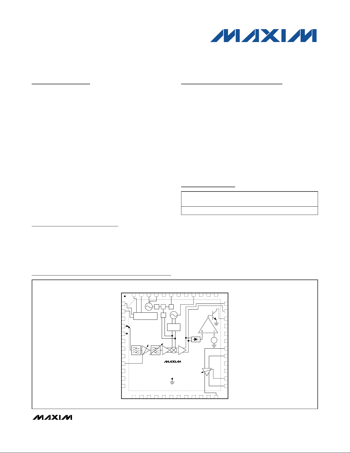
The MAX3541 complete single-conversion television
tuner is designed for use in analog/digital terrestrial applications and digital set-top boxes. This television tuner
draws only 760mW of power from a +3.3V supply voltage.
The MAX3541 is designed to convert PAL or DVB-C signals in the 47MHz to 68MHz, 174MHz to 230MHz, and
470MHz to 862MHz bands to an intermediate frequency
(IF) of 36MHz.
The MAX3541 includes a variable-gain low-noise amplifier (LNA), multiband tracking filters, a harmonic-rejection
mixer, a low-noise IF amplifier, an IF power detector, and
a variable-gain IF amplifier. The MAX3541 also includes
fully monolithic VCOs and tank circuits, as well as a
complete frequency synthesizer. This highly integrated
design allows for low-power tuner-on-board applications
without the cost and power dissipation issues of dualconversion tuner solutions.
The MAX3541 is specified for operation in the -40°C to
+85°C temperature range and is available in a leadless
48-pin flip-chip (fcLGA) package.
Applications
Televisions
Analog/Digital Terrestrial Receivers
Digital Set-Top Boxes
Features
♦ Low Power Consumption: 760mW (typ) from a
+3.3V Supply Voltage
♦ Integrated Tracking Filters
♦ Low Noise Figure: 4.9dB (typ)
♦ Small 7mm x 7mm fcLGA Leadless Package
♦ IF Overload Detector Controls RF Variable-Gain
Amplifier
♦ 2-Wire, I
2
C-Compatible Serial Control Interface
MAX3541
Complete Single-Conversion
Television Tuner
________________________________________________________________
Maxim Integrated Products
1
Ordering Information
19-1029; Rev 0; 10/07
For pricing, delivery, and ordering information, please contact Maxim Direct at 1-888-629-4642,
or visit Maxim’s website at www.maxim-ic.com.
*
EP = Exposed paddle.
#
Indicates RoHS-compliant and exempt from lead-free
requirements.
Pin Configuration/Functional Diagram
PART
TEMP
RANGE
M AX 3541E LM #G42 - 40° C to + 85° C 48 fcLG A- E P * L4877F- A
PINPACKAGE
PKG
CODE
XTALPGND
÷ R PD CP
CC
XTALNGND
V
÷ N
DIVIDER
MAX3541
GND
ADDR2GND
ADDR1GND
SCL
SERIAL
3V
CC
4UHF_IN
5VHF_IN
6RFGND2
7LEXT
8RFGND3
9RFAGC
10V
CC
12GND
INTERFACE
1348144715461645174418431942204121402239233824
CC
CPGND
MUXGND
V
VTUNEGND
VCO
EP
GND
CC
GND_TUNEGND
LDOV
V
37
36 IFOUT1-1
35 IFOUT1+2SDA
34 IFOVLD
33 V
CC
32 V
CC
V
REF
+
31 GND
-
30 IFIN+
29 IFIN-
28 V
CC
27 GND
26 IFAGC11GND
25 IFOUT2+
CC
IFOUT2-
Page 2
MAX3541
Complete Single-Conversion
Television Tuner
2 _______________________________________________________________________________________
ABSOLUTE MAXIMUM RATINGS
DC ELECTRICAL CHARACTERISTICS
(MAX3541 EV kit, VCC= +3.1V to +3.5V, TA= -40°C to +85°C, no RF signals at RF inputs, default register settings, V
RFAGC
= V
IFAGC
= +3V (minimum attenuation), unless otherwise noted. Typical values are at VCC= +3.3V, TA= +25°C, unless otherwise noted.)
Stresses beyond those listed under “Absolute Maximum Ratings” may cause permanent damage to the device. These are stress ratings only, and functional
operation of the device at these or any other conditions beyond those indicated in the operational sections of the specifications is not implied. Exposure to
absolute maximum rating conditions for extended periods may affect device reliability.
VCCto GND..............................................................-0.3V, +3.6V
RFIN, IFIN_ IFOUT1_, IFOUT2_, IFAGC, RFAGC,
VTUNE, LDO, MUX, CP,
XTAL to GND....................................-0.3V to (V
CC
+ 0.3V)
SDA, SCL, ADDR2, ADDR1 to GND......................-0.3V to +3.6V
IFOUT__ Short-Circuit Duration .....................................Indefinite
RF Input Power ...............................................................+10dBm
Continuous Power Dissipation (T
A
= +70°C)
48-Pin fcLGA (derate 25mW/°C above +70°C) ..............1.4W
Operating Temperature Range ...........................-40°C to +85°C
Junction Temperature......................................................+150°C
Storage Temperature Range .............................-65°C to +165°C
CAUTION! ESD SENSITIVE DEVICE
PARAMETER CONDITIONS MIN TYP MAX UNITS
SUPPLY VOLTAGE AND CURRENT
Supply Voltage +3.1 +3.5 V
Supply Current
RF and IF AG C Inp ut Bi as C ur r ent At +0.5V and +3V -50 +50 μA
RF and IF AGC Control Voltage (Note 1)
Digital Input Logic-Level Low 0.3 x V
Digital Input Logic-Level High 0.7 x V
SERIAL INTERFACE
Input Logic-Level Low 0.3 x V
Input Logic-Level High 0.7 x V
Input Hysteresis 0.05 x V
SDA, SCL Input Current -10 +10 μA
Output Logic-Level Low 3mA sink current 0.4 V
Output Logic-Level High VCC - 0.5 V
Receive mode (SHDN = 3V) 230 275
Shutdown mode (SHDN = 0V) 5
Minimum attenuation +3
Maximum attenuation +0.5
CC
CC
CC
CC
CC
mA
V
V
V
V
V
V
Page 3
MAX3541
Complete Single-Conversion
Television Tuner
_______________________________________________________________________________________ 3
AC ELECTRICAL CHARACTERISTICS
(MAX3541 EV kit, VCC= +3.1V to +3.5V, TA= -40°C to +85°C, 75Ω system impedance, default register settings, V
RFAGC
= V
IFAGC
=
+3V (minimum attenuation), unless otherwise noted. Typical values are at V
CC
= +3.3V, TA= +25°C, unless otherwise noted.)
PARAMETER CONDITIONS MIN TYP MAX UNITS
RF INPUT TO IFOUT1 OUTPUT
Operating Frequency Range
(see Table 7)
Output Frequency
Voltage Gain
Input Return Loss Selected channel 10 dB
Noise Figure Maximum gain (V
Input IP2 (In-Band and Out-of-Band Tones)
Input IP3 (In-Band and Out-of-Band Tones)
Input P
1dB
Beats Within Output 0dBmV PIX carrier level -40 dBc
Beats, Converted to Output
Gain Flatness 47MHz to 54MHz 2.5 dB
Isolation
Port-to-Port Isolation Isolation between RF input ports at 215MHz 27 dB
Image Rejection
Spurious Leakage at RF Input
Phase Noise (Single-Sideband)
Output Return Loss Balanced 50Ω load 20 dB
IF VARIABLE-GAIN AMPLIFIER
Input Impedance Balanced 2000 Ω
Output Impedance Balanced (Note 1) 300 Ω
Gain specification met across these
frequency bands
Analog channel PIX carrier 38.9
Digital channel center frequency 36
Source impedance
= 75Ω, load
impedance = 200Ω
RFAGC
Maximum gain (V
RFAGC
At 12.5dB of gain 30
Maximum gain (V
RFAGC
At 12.5dB of gain 10
Maximum gain (V
RFAGC
At 12.5dB of gain -5
VHF input, 140MHz to 500MHz -60
VHF input, 500MHz to 1400MHz -50
UHF input, 950MHz to 1400MHz -60
5MHz to 50MHz, RF input to IF output,
relative to desired channel
Measured at 77.8MHz above desired
channel’s center frequency
5Hz to 65MHz -40
65MHz to 878MHz -40
1kHz -80
10kHz offset -85
100kHz offset (1.5kHz loop bandwidth) -105
1MHz offset (1.5kHz loop bandwidth) -125
47 68
174 230
470 862
Maximum gain
(V
Minimum gain
(V
= 3V)
RAVGC
= 0.5V)
RAVGC
= 3V) 4.9 dB
= 3V) 20
= 3V) -10
= 3V) -38
33 41 49
-10
60 dBc
57 70 dBc
MHz
MHz
dB
dBm
dBm
dBm
dBc
P-P
dBmV
dBc/Hz
Page 4
MAX3541
Complete Single-Conversion
Television Tuner
4 _______________________________________________________________________________________
AC ELECTRICAL CHARACTERISTICS (continued)
(MAX3541 EV kit, VCC= +3.1V to +3.5V, TA= -40°C to +85°C, 75Ω system impedance, default register settings, V
RFAGC
= V
IFAGC
=
+3V (minimum attenuation), unless otherwise noted. Typical values are at V
CC
= +3.3V, TA= +25°C, unless otherwise noted.)
Note 1: Guaranteed by design and characterization.
PARAMETER CONDITIONS MIN TYP MAX UNITS
S our ce l oad =
Passband Voltage Gain
1.1kΩ,
output load = 1kΩ
Passband Gain Flatness 32MHz to 40MHz (Note 1) 1.2 dB
Output Voltage V
AGC Gain Slope V
Equivalent Input Voltage Noise Density
Noise Figure Change vs. Attenuation < 0.35 dB/dB
IM3 V
IF OVERLOAD DETECTOR (See the IF Overload Detector Section)
Output Overload Attack Point 0.7 V
Attack Point Accuracy OD REG = 3 ±1 dB
Detector Output Voltage Range
Detector Gain 70 V/V
FREQUENCY SYNTHESIZER
REFERENCE OSCILLATOR
Frequency 8 MHz
DIVIDERS
RF N-Divider Ratio 256 32,767
RF R-Divider Ratio 16 127
LO PHASE DETECTOR AND CHARGE PUMP
Comparison Frequency 63 250 kHz
Charge-Pump Current
Charge-Pump Three-State Current ±5 nA
Charge-Pump Compliance Range 0.4
Charge-Pump Current Matching 5%
LOCAL OSCILLATOR
VCO Tuning Range Tank frequency 2200 4400 MHz
VCO Tuning Gain Tank oscillator gain 500 MHz/V
2-WIRE SERIAL INTERFACE
Clock Frequency 400 kHz
= 3V (Note 1) 2.5 V
IFAGC
= 3V to 0.5V (Note 1) 27 dB/V
IFAGC
At 36MHz, maximum gain (V
(Note 1)
= 1V
OUT
Negative polarity, overload reduces V
(open collector, 0.3mA sink)
CP = 00 0.5
CP = 01 1
CP = 10 1.5
CP = 11 2
, 40dB < gain < 60dB (Note 1) -56 dBc
P-P
Maximum gain setting
= 3V)
(V
IFAGC
Minimum gain setting
= 0.5V)
(V
IFAGC
= 3V)
IFAGC
DET
54 59 63
0.5 3.0 V
21
7.3 nV/√Hz
V
-
CC
0.4
dB
P-P
P-P
mA
V
Page 5
MAX3541
Complete Single-Conversion
Television Tuner
_______________________________________________________________________________________
5
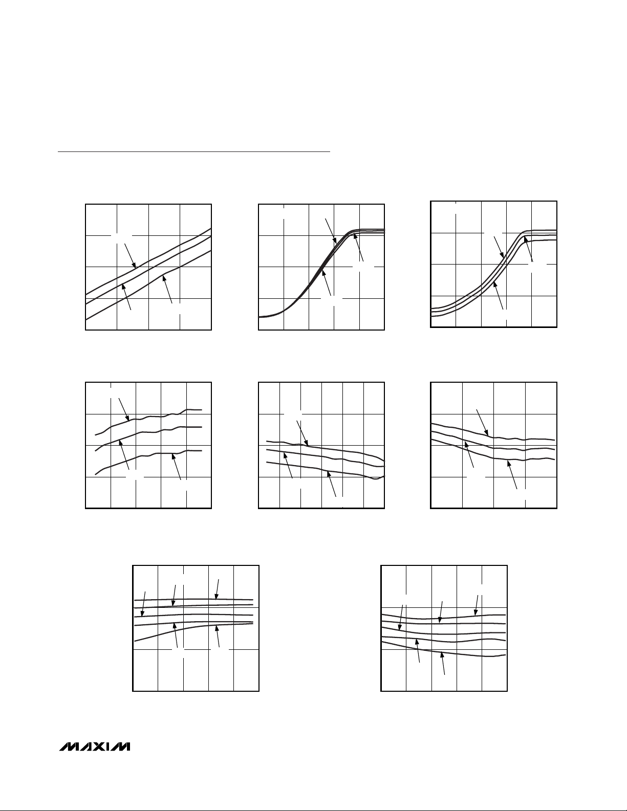
Typical Operating Characteristics
(MAX3541EV kit, VCC= +3.3V, V
IFAGC
= 3.0V, V
RFAGC
= 3.0V, TA= +25°C, unless otherwise noted.)
VHF NOISE FIGURE vs. FREQUENCY
FREQUENCY (MHz)
NOISE FIGURE (dB)
MAX3541 toc07
48 51 54 57 60 63
1
3
5
7
+25°C
-40°C
+85°C
+55°C
0°C
SUPPLY CURRENT vs. SUPPLY VOLTAGE
208
204
200
SUPPLY CURRENT (mA)
196
192
3.1 3.2 3.3 3.4 3.5
+85°C
+25°C
SUPPLY VOLTAGE (V)
-40°C
VHF VOLTAGE GAIN vs. FREQUENCY
46
-40°C
44
MAX3541 toc01
MAX3541 toc04
VHF VOLTAGE GAIN vs. RFAGC VOLTAGE
60
fRF = 64.5MHz
40
20
VHF VOLTAGE GAIN (dB)
0
-20
0.5 1.0 1.5 2.0 2.5 3.0
VHF VOLTAGE GAIN vs. FREQUENCY
55
50
-40°C
+25°C
+85°C
RFAGC VOLTAGE (V)
-40°C
60
MAX3541 toc02
40
20
UHF VOLTAGE GAIN (dB)
0
-20
60
MAX3541 toc05
50
UHF VOLTAGE GAIN vs. RFAGC VOLTAGE
fRF = 801MHz
-40°C
+25°C
+85°C
0.5 1.0 1.5 2.0 2.5 3.0
RFAGC VOLTAGE (V)
UHF VOLTAGE GAIN vs. FREQUENCY
-40°C
MAX3541 toc03
MAX3541 toc06
42
VHF VOLTAGE GAIN (dB)
40
38
45 50 55 60 65 70
+25°C
FREQUENCY (MHz)
+85°C
45
VHF VOLTAGE GAIN (dB)
40
35
170 180 190 200 210 220 230
+25°C
+85°C
FREQUENCY (MHz)
40
UHF VOLTAGE GAIN (dB)
30
20
470 570 670 770 870
+25°C
FREQUENCY (MHz)
VHF NOISE FIGURE vs. FREQUENCY
7
+25°C
5
3
NOISE FIGURE (dB)
1
175 185 195 205 215 225
+55°C
0°C
-40°C
FREQUENCY (MHz)
+85°C
+85°C
MAX3541 toc08
Page 6
MAX3541
Complete Single-Conversion
Television Tuner
6 _______________________________________________________________________________________
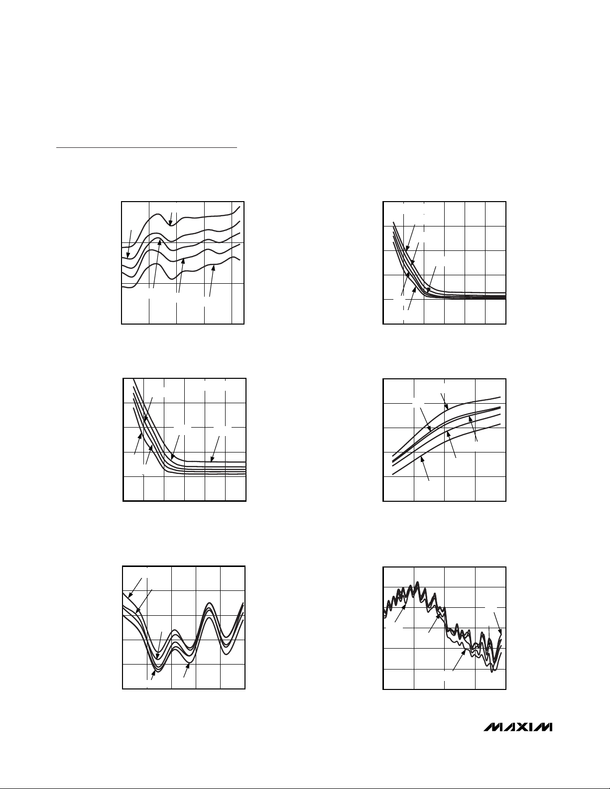
Typical Operating Characteristics (continued)
(MAX3541EV kit, VCC= +3.3V, V
IFAGC
= 3.0V, V
RFAGC
= 3.0V, TA= +25°C, unless otherwise noted.)
UHF NOISE FIGURE vs. FREQUENCY
FREQUENCY (MHz)
NOISE FIGURE (dB)
MAX3541 toc09
470 560 650 740 830
1
3
5
7
+55°C
+85°C
+25°C
0°C
-40°C
VHF NOISE FIGURE vs. RFAGC VOLTAGE
RFAGC VOLTAGE (V)
NOISE FIGURE (dB)
MAX3541 toc10
1.8 2.0 2.2 2.4 2.6 2.8 3.0
0
4
8
12
16
20
fRF = 224.25MHz
+55°C
+85°C
+25°C
0°C
-40°C
UHF NOISE FIGURE vs. RFAGC VOLTAGE
RFAGC VOLTAGE (V)
NOISE FIGURE (dB)
MAX3541 toc11
1.8 2.0 2.2 2.4 2.6 2.8 3.0
0
4
8
12
16
20
fRF = 631.25MHz
+55°C
+85°C
+25°C
0°C
-40°C
VHF IMAGE REJECTION vs. FREQUENCY
FREQUENCY (MHz)
VHF IMAGE REJECTION (dB)
MAX3541 toc12
47 51 55 59 63
70
72
74
76
78
80
-40°C
0°C
+85°C
+55°C
+25°C
VHF IMAGE REJECTION vs. FREQUENCY
FREQUENCY (MHz)
VHF IMAGE REJECTION (dB)
MAX3541 toc13
175 185 195 205 215 225
72
73
74
75
76
77
+25°C
-40°C
+85°C
+55°C
0°C
UHF IMAGE REJECTION vs. FREQUENCY
FREQUENCY (MHz)
UHF IMAGE REJECTION (dB)
MAX3541 to14
470 570 670 770 870
64
66
68
70
72
74
76
+25°C
-40°C
+85°C
+55°C
0°C
Page 7

MAX3541
Complete Single-Conversion
Television Tuner
_______________________________________________________________________________________
7
Typical Operating Characteristics (continued)
(MAX3541EV kit, VCC= +3.3V, V
IFAGC
= 3.0V, V
RFAGC
= 3.0V, TA= +25°C, unless otherwise noted.)
VHF-L PHASE NOISE AT 10kHz OFFSET
vs. CHANNEL FREQUENCY
-95
-97
-99
-101
VHF-L PHASE NOISE (dBc/Hz)
-103
-105
45 50 55 60 65 70
CHANNEL FREQUENCY (MHz)
UHF PHASE NOISE AT 10kHz OFFSET
vs. CHANNEL FREQUENCY
-80
-83
-86
-89
VHF-L PHASE NOISE AT 10kHz OFFSET
vs. CHANNEL FREQUENCY
MAX3541 toc16
170 180 190 200 210 220 230 240
CHANNEL FREQUENCY (MHz)
VHF PHASE NOISE vs. OFFSET FREQUENCY
fRF = 64.5MHz
MAX3541 toc18
MAX3541 toc15
MAX3541 toc17
-90
-92
-94
-96
VHF-L PHASE NOISE (dBc/Hz)
-98
-100
-60
-80
-100
UHF PHASE NOISE (dBc/Hz)
-92
-95
400 500 600 700 800 900
CHANNEL FREQUENCY (MHz)
-120
VHF PHASE NOISE (dBc/Hz)
-140
0.1 1 10 100 1000
OFFSET FREQUENCY (kHz)
IFOUT1 NORMALIZED FREQUENCY RESPONSE
UHF PHASE NOISE vs. OFFSET FREQUENCY
-60
fRF = 801MHz
-70
-80
-90
-100
-110
UHF PHASE NOISE (dBc/Hz)
-120
-130
0.1 1 10 100 1000
OFFSET FREQUENCY (kHz)
MAX3541 toc19
5
0
-5
-10
IFOUT1 POWER (dBm)
-15
-20
1 10 100 1000
(5MHz to 200MHz)
FREQUENCY (MHz)
MAX3541 toc20
Page 8

MAX3541
Complete Single-Conversion
Television Tuner
8 _______________________________________________________________________________________
Pin Description
Typical Operating Characteristics (continued)
(MAX3541EV kit, VCC= +3.3V, V
IFAGC
= 3.0V, V
RFAGC
= 3.0V, TA= +25°C, unless otherwise noted.)
IFVGA VOLTAGE GAIN vs. IFAGC VOLTAGE
60
50
40
30
IFVGA VOLTAGE GAIN (dB)
20
10
0.5 1.0 1.5 2.0 2.5 3.0
IFAGC VOLTAGE (V)
-40°C
MAX3541 toc21
+25°C
+85°C
PIN NAME DESCRIPTION
1 SCL 2-Wire Serial-Clock Interface. Requires a pullup resistor to VCC.
2 SDA 2-Wire Serial-Data Interface. Requires a pullup resistor to VCC.
3, 10, 23, 28,
32, 33, 37,
V
CC
Power Supply Connections. Bypass each supply pin to ground with a 1000pF capacitor.
41, 44
4 UHF_IN UHF RF Input. Requires a DC-blocking capacitor.
5 VHF_IN VHF RF Input. Requires a DC-blocking capacitor.
6 RFGND2
RF Ground. Bypass to the PCB’s ground plane with a 1000pF capacitor. Do not connect RFGND2
and RFGND3 together.
7 LEXT RF VGA Supply Voltage. Connect through a 270nH pullup inductor to VCC.
8 RFGND3
RF Ground. Bypass to the PCB’s ground plane with a 1000pF capacitor. Do not connect RFGND2
and RFGND3 together.
9 RFAGC RF V G A G ai n C ontr ol V ol tag e. Accep ts a D C vol tag e fr om 0.5V ( m i ni m um g ai n) to 3V ( m axi m um g ai n) .
11–22, 27, 31 GND Ground. Connect to the PCB’s ground plane.
24 IFOUT2- Inver ti ng IF V G A Outp ut. C onnect to the i np ut of an anti - al i asi ng fi l ter . Req ui r es a D C - b l ocki ng cap aci tor .
25 IFOUT2+ N oni nver ti ng IF V GA O utp ut. C onnect to the i np ut of an anti - al i asi ng fi l ter . Req ui r es a D C - b l ocki ng cap aci tor .
26 IFAGC IF VGA Gain Control Voltage. Accepts a DC voltage from 0.5V (minimum gain) to 3V (maximum gain).
29 IFIN- Inverting IF VGA Input. Connect to the output of an IF-SAW filter.
30 IFIN+ Noninverting IF VGA Input. Connect to the output of an IF-SAW filter.
34 IFOVLD IF Overload Detector Open-Collector Output. Requires a 10kΩ pullup resistor to VCC.
35 IFOUT1+ Noninverting IF LNA Output. Requires a DC-blocking capacitor.
36 IFOUT1- Inverting IF LNA Output. Requires a DC-blocking capacitor.
38 LDO VCO LDO Bypass. Bypass to ground with a 0.47μF capacitor.
IFVGA IM3 vs. IFAGC VOLTAGE
-20
-30
-40
IFVGA IM3 (dBc)
-50
IM3
-60
0.5 1.0 1.5 2.0 2.5 3.0
IFAGC VOLTAGE (V)
PIN
V
OUT
MAX3541 toc22
= 1.5 V
-20
P-P
-40
-60
INPUT POWER (dBm)
-80
Page 9

MAX3541
Complete Single-Conversion
Television Tuner
_______________________________________________________________________________________ 9
Pin Description (continued)
PIN NAME DESCRIPTION
39 GND_TUNE
40 VTUNE VCO Tuning Input. Connect to the PLL loop filter output.
42 MUX Test Output. Leave this pin unconnected during normal operation.
43 CP Charge-Pump Output. Connect to PLL loop filter input.
45 XTALN Crystal Oscillator Feedback. See the Typical Application Circuit.
46 XTALP Crystal Oscillator Feedback. See the Typical Application Circuit.
47 ADDR1
48 ADDR2
EP GND Exposed Paddle. Solder evenly to the PCB ground plane for proper operation.
VTUNE Ground Connection. Connect to the PCB ground plane. All loop filter component GNDs must
be connected to this pin (see the Typical Application Circuit).
2-Wire Serial-Interface Address Line 1. This pin along with ADDR2 sets the device address for the
2
C-compatible serial interface.
I
2-Wire Serial-Interface Address Line 2. This pin along with ADDR1 sets the device address for the
2
I
C-compatible serial interface.
Page 10

MAX3541
Detailed Description
Register Descriptions
The MAX3541 includes 11 programmable registers and
2 read-only registers. The 11 programmable registers
include two N-divider registers, an R-divider register, a
VCO register, an IFOVLD/Charge Pump/Filter Select
register, a Control register, a Shutdown register, and
Tracking Filter Control registers. These 11 programmable registers are also readable. The read-only registers
include a status register and a ROM table data register.
Recommended default bit settings are provided for
user convenience only and are not guaranteed. The
user must write all registers after power-up and no earlier than 100μs after power-up.
Complete Single-Conversion
Television Tuner
10 ______________________________________________________________________________________
Table 1. Register Configuration
Table 2. N-DIV High Register (Address: 0000b)
REGISTER
NAME
N-DIV High Both 0x00 0 N14 N13 N12 N11 N10 N9 N8
N-DIV Low Both 0x01 N7 N6 N5 N4 N3 N2 N1 N0
R-DIV Both 0x02 0 R6 R5 R4 R3 R2 R1 R0
VCO Both 0x03 VCO4 VCO3 VCO2 VCO1 VCO0 LD VDIV1 VDIV0
IFO V LD ,
C har g e P um p ,
and Fi l ter S el ect
Control Both 0x05 0 0 0 0
Shutdown Both 0x06
Tr acki ng Fi l ter
S er i es C ap aci tor
Tracking Fi l ter
P ar al lel Cap acitor
Tracking Filter
ROM Address
Reserved Both 0x0A X X X X X X X X
ROM Table
Data Readback
Status Read 0x0C POR LD2 LD1 LD0 X X X X
READ/
WRITE
Read 0x0B TFR7 TFR6 TFR5 TFR4 TFR3 TFR2 TFR1 TFR0
REGISTER
ADDRESS
Both 0x04 0 IFOVLD2 IFOVLD1 IFOVLD0 CP1 CP0 TF 0
Both 0x07 TFS7 TFS6 TFS5 TFS4 TFS3 TFS2 TFS1 TFS0
Both 0x08 FLD 0 TFP5 TFP4 TFP3 TFP2 TFP1 TFP0
Both 0x09 0 0 0 0 TFA3 TFA2 TFA1 TFA0
MSB LSB
D7 D6 D5 D4 D3 D2 D1 D0
SHDN
_MIX1
SHDN
_MIX0
DATA BYTE
SHDN
_IF
SHDN
_OD
SHDN
_RF
SHDN
_SYN
SHDN
_IFVGA
000
INPT1 INPT0
BIT NAME BIT LOCATION (0 = LSB)
RESERVED 7 0 Must be set to 0.
N[14:8] 6-0 0000001
RECOMMENDED
DEFAULT
Sets the most significant bits of the PLL integer divider (N). Default
integer divider value is N = 4688. N can range from 256 to 32,767.
FUNCTION
Page 11

MAX3541
Complete Single-Conversion
Television Tuner
______________________________________________________________________________________ 11
Table 3. N-DIV Low Register (Address: 0001b)
Table 4. R-DIV Register (Address: 0010b)
Table 5. VCO Register (Address: 0011b)
BIT NAME BIT LOCATION (0 = LSB)
N[7:0] 7-0 10101011
RECOMMENDED
DEFAULT
Sets the least significant bits of the PLL integer divider (N). Default
integer divider value is N = 4688. N can range from 256 to 32,767.
BIT NAME BIT LOCATION (0 = LSB)
RESERVED 7 0 Must be set to 0.
R[6:0] 6-0 0010000
RECOMMENDED
DEFAULT
Sets the PLL reference divider (R). Default reference divider value is
R = 64. R can range from 16 to 127.
BIT NAME BIT LOCATION (0 = LSB)
VCO[4:3] 7-6 10
VCO[2:0] 5-3 111
LD 2 1
VDIV[1:0] 1-0 10
RECOMMENDED
DEFAULT
VCO select. Selects one of three possible VCOs.
00 = VCOs shut down
01 = Selects VCO1
10 = Selects VCO2
11 = Selects VCO3
V C O sub - b and sel ect. S el ects one of ei g ht p ossi b l e V C O sub - b and s.
000 = Selects SB0
001 = Selects SB1
010 = Selects SB2
011 = Selects SB3
100 = Selects SB4
101 = Selects SB5
110 = Selects SB6
111 = Selects SB7
Lock detect enable.
0 = Disabled
1 = Enabled
VCO divider ratio select.
00 = S ets V C O d i vi d er to 4
01 = S ets V CO d i vi d er to 8
10 = Sets VCO divider to 16
11 = Sets VCO divider to 32
FUNCTION
FUNCTION
FUNCTION
Page 12

MAX3541
Complete Single-Conversion
Television Tuner
12 ______________________________________________________________________________________
Table 6. IFOVLD, Charge Pump, and Filter Select Register (Address: 0100b)
Table 7. Control Register (Address: 0101b)
Table 8. Shutdown Register (Address: 0110b)
BIT NAME BIT LOCATION (0 = LSB)
RESERVED 7 0 Must be set to 0.
IFOVLD[2:0] 6-4 000 Write content of ROM register OD[2:0] to this location.
CP[1:0] 3-2 00
TF 1 0
RESERVED 0 0 Must be set to 0.
RECOMMENDED
DEFAULT
Selects the typical charge-pump current.
00 = 0.5mA
01 = 1mA
10 = 1.5mA
11 = 2mA
Selects the tracking filter band of operation.
0 = VHF
1 = UHF
BIT NAME BIT LOCATION (0 = LSB)
RESERVED 7-4 0000 Must be set to 0000.
SHDN_RF 3 0
S H DN _IFV GA 2 0
INPT[1:0] 1-0 01
RECOMMENDED
DEFAULT
RF shutdown.
0 = RF circuitry enabled
1 = RF circuitry disabled
IF VGA shutdown.
0 = IF VGA enabled
1 = IF VGA disabled
Selects the RF input.
00 = Selects VHF_IN, LPF enabled
01 = Selects VHF_IN, LPF disabled
10 = Selects UHF_IN
11 = Factory use only
FUNCTION
FUNCTION
BIT NAME BIT LOCATION (0 = LSB)
SHDN_MIX 7-6 00
SHDN_IF 5 0
SHDN_OD 4 0
SHDN_SYN 3 0
RESERVED 2-0 000 Must be set to 000.
RECOMMENDED
DEFAULT
Mixer shutdown.
00 = Mixer enabled
01,10 = Factory use only
11 = Mixer disabled
IF shutdown.
0 = IF section enabled
1 = IF section disabled
IFOVLD shutdown.
0 = Power detector enabled
1 = Power detector disabled
Frequency synthesizer shutdown.
0 = Synthesizer enabled
1 = Synthesizer disabled
FUNCTION
Page 13

MAX3541
Complete Single-Conversion
Television Tuner
______________________________________________________________________________________ 13
Table 9. Tracking Filter Series Capacitor Register (Address: 0111b)
*See the
RF Tracking Filter
section.
Table 13. ROM Table Data Readback Register (Address: 1011b)
*See the
RF Tracking Filter
section.
Table 12. Reserved Register (Address: 1010b)
*See the
RF Tracking Filter
section.
*See the
RF Tracking Filter
section.
Table 10. Tracking Filter Parallel Capacitor Register (Address: 1000b)
Table 11. Tracking Filter ROM Address Register (Address: 1001b)
Table 14. Status Register (Address: 1100b)
BIT NAME BIT LOCATION (0 = LSB)
TFS[7:0] 7-0 00001111* Programs series capacitor values in the tracking filter.
RECOMMENDED
DEFAULT
FUNCTION
BIT NAME BIT LOCATION (0 = LSB)
FLD 7 0
RESERVED 6 0 Must be set to 0.
TFP[5:0] 5-0 001001* Programs parallel capacitor values in the tracking filter.
RECOMMENDED
DEFAULT
Filter load bit. A 0 to 1 transition of this bit forces the loading of the
ROM Table Data Readback register.
FUNCTION
BIT NAME BIT LOCATION (0 = LSB)
RESERVED 7-4 0000 Must be set to 0000.
TFA[3:0] 3-0 0000* Address bits of the ROM register to be read.
RECOMMENDED
DEFAULT
FUNCTION
BIT NAME BIT LOCATION (0 = LSB)
RESERVED 7-0 N/A Reserved. Do not program these bits during normal operation.
RECOMMENDED
DEFAULT
FUNCTION
BIT NAME BIT LOCATION (0 = LSB)
TFR[7:0] 7-0 00000000* Tracking filter data bits read from the device’s ROM table.
RECOMMENDED
DEFAULT
FUNCTION
BIT NAME BIT LOCATION (0 = LSB)
POR 7 N/A
LD[2:0] 6-4 N/A
RESERVED 3-0 N/A Reserved.
RECOMMENDED
DEFAULT
Power-on reset.
0 = Status register has been read
1 = Power reset since last status register read
VCO tuning voltage indicators.
000 = PLL not in lock, tune to the next lowest sub-band
001–110 = PLL in lock
111 = PLL not in lock, tune to the next higher sub-band
FUNCTION
Page 14

MAX3541
2-Wire Serial Interface
The MAX3541 use a 2-wire I2C-compatible serial interface consisting of a serial-data line (SDA) and a serialclock line (SCL). SDA and SCL facilitate bidirectional
communication between the MAX3541 and the master at
clock frequencies up to 400kHz. The master initiates a
data transfer on the bus and generates the SCL signal to
permit data transfer. The MAX3541 behaves as a slave
device that transfers and receives data to and from the
master. Pull SDA and SCL high with external pullup
resistors (1kΩ or greater) for proper bus operation.
One bit is transferred during each SCL clock cycle. A
minimum of nine clock cycles is required to transfer a
byte in or out of the MAX3541 (8 data bits and an
ACK/NACK). The data on SDA must remain stable during
the high period of the SCL clock pulse. Changes in SDA
while SCL is high and stable are considered control signals (see the
START and STOP Conditions
section). Both
SDA and SCL remain high when the bus is not busy.
START and STOP Conditions
The master initiates a transmission with a START condition (S), which is a high-to-low transition on SDA while
SCL is high. The master terminates a transmission with
a STOP condition (P), which is a low-to-high transition
on SDA while SCL is high.
Acknowledge and Not-Acknowledge Conditions
Data transfers are framed with an acknowledge bit
(ACK) or a not-acknowledge bit (NACK). Both the master and the MAX3541 (slave) generate acknowledge
bits. To generate an acknowledge, the receiving device
must pull SDA low before the rising edge of the
acknowledge-related clock pulse (ninth pulse) and
keep it low during the high period of the clock pulse.
To generate a not-acknowledge condition, the receiver
allows SDA to be pulled high before the rising edge of
the acknowledge-related clock pulse, and leaves SDA
high during the high period of the clock pulse.
Monitoring the acknowledge bits allows for detection of
unsuccessful data transfers. An unsuccessful data
transfer happens if a receiving device is busy or if a
system fault has occurred. In the event of an unsuccessful data transfer, the bus master must reattempt
communication at a later time.
Slave Address
The MAX3541 has a 7-bit slave address that must be
sent to the device following a START condition to initiate communication. The slave address is determined
by the state of the ADDR2 and ADDR1 pins and is
equal to 11000[ADDR2][ADDR1]. The eighth bit (R/W)
following the 7-bit address determines whether a read
or write operation occurs. Table 15 shows the possible
address configurations.
The MAX3541 continuously awaits a START condition
followed by its slave address. When the device recognizes its slave address, it acknowledges by pulling the
SDA line low for one clock period; it is ready to accept
or send data depending on the R/W bit (Figure 1).
Complete Single-Conversion
Television Tuner
14 ______________________________________________________________________________________
Figure 1. MAX3541 Slave Address Byte
Table 15. MAX3541 Address Configurations
ADDR2 ADDR1 WRITE ADDRESS READ ADDRESS
0 0 0xC0 0xC1
0 1 0xC2 0xC3
1 0 0xC4 0xC5
1 1 0xC6 0xC7
SLAVE ADDRESS
S 1 1 0 0 0 ADDR2 ADDR1 R/W ACK
SDA
SCL
NOTE: TIMING PARAMETERS CONFORM WITH I2C BUS SPECIFICATIONS.
123456789
P
Page 15

Write Cycle
When addressed with a write command, the MAX3541
allows the master to write to a single register or to multiple successive registers.
A write cycle begins with the bus master issuing a
START condition followed by the seven slave address
bits and a write bit (R/W = 0). The MAX3541 issues an
ACK if the slave address byte is successfully received.
The bus master must then send to the slave the
address of the first register it wishes to write to. If the
slave acknowledges the address, the master can then
write one byte to the register at the specified address.
Data is written beginning with the most significant bit.
The MAX3541 again issues an ACK if the data is successfully written to the register. The master can continue to write data to the successive internal registers with
the MAX3541 acknowledging each successful transfer,
or it can terminate transmission by issuing a STOP condition. The write cycle does not terminate until the master issues a STOP condition.
Figure 2 illustrates an example in which registers 0
through 2 are written with 0x0E, 0xD8, and 0xE1,
respectively.
Read Cycle
A read cycle begins with the bus master issuing a
START condition followed by the seven slave address
bits and a write bit (R/W = 0). The MAX3541 issues an
ACK if the slave address byte is successfully
received. The master then sends the 8-bit address of
the first register that it wishes to read. The MAX3541
then issues another ACK. Next, the master must issue
a START condition followed by the 7 slave address
bits and a read bit (R/W = 1). The MAX3541 issues an
ACK if it successfully recognizes its address and
begins sending data from the specified register
address starting with the most significant bit (MSB).
Data is clocked out of the MAX3541 on the rising
edge of SCL. On the 9th rising edge of SCL, the master can issue an ACK and continue reading successive registers or it can issue a NACK followed by a
STOP condition to terminate transmission. The read
cycle does not terminate until the master issues a
STOP condition. Figure 3 illustrates an example in
which registers 0 and 1 are read back.
MAX3541
Complete Single-Conversion
Television Tuner
______________________________________________________________________________________ 15
Figure 2. Example: Write Registers 0 Through 2 with 0x0E, 0xD8, and 0xE1, Respectively
Figure 3. Example: Read Data from Registers 0 and 1
WRITE DEVICE
START
ADDRESS
11000[ADDR2][ADDR1] 0 —————
R/W
WRITE REGISTER
ACK ACK ACK ACK ACK
ADDRESS
0x00
WRITE DATA TO
REGISTER 0x00
0x0E
WRITE DATA TO
REGISTER 0x01
0xD8
WRITE DATA TO
REGISTER 0x02
0xE1
STOP
WRITE DEVICE
START
ADDRESS
110000[ADDR2][ADDR1]
R/W
WRITE 1ST REGISTER
ACK NACK
ADDRESS
0x00
ACK
—
START
WRITE DEVICE
110000[ADDR2][ADDR1]0 ——
ADDRESS
R/W
1—
ACK
READ DATA
REG 0
D7–D0
ACK
—
READ DATA
REG 1
D7–D0
STOP
Page 16

MAX3541
Application Information
RF Inputs
The MAX3541 features separate UHF and VHF inputs
that are matched to 75Ω. Both inputs require a DCblocking capacitor. The active inputs are selected by
the input registers. In addition, the input registers
enable or disable the lowpass filter, which can be used
when the VHF input is selected. For the 47MHz to
68MHz, select the VHF_IN with the LPF filter enabled
(INPT = 00). For 174MHz to 230MHz, select VHF_IN
with LPF disabled (INPT = 01). For 470MHz to 862MHz,
select UHF_IN (INPT = 10).
RF Gain Control
The gain of the RF low-noise amplifier can be adjusted
over a typical range of 45dB with the RFAGC pin. The
RFAGC input accepts a DC voltage from 0.5V to 3V,
with 3V providing maximum gain. This pin can be controlled with the IF power-detector output to form a
closed RF gain-control loop. See the
Closed-Loop RF
Gain Control
section for more information.
RF Tracking Filter
The MAX3541 includes a programmable tracking filter
for each band of operation to optimize rejection of
out-of-band interference while minimizing insertion
loss for the desired received signal. The center frequency of each tracking filter is selected by a
switched-capacitor array that is programmed by the
TFS[7:0] bits in the Tracking Filter Series Capacitor
register and the TFP[5:0] bits in the Tracking Filter
Parallel Cap register.
Optimal tracking filter settings for each channel varies
from part to part due to process variations. To accommodate part-to-part variations, each part is factory calibrated by Maxim. During calibration, the y-intercept
and slope for the series and parallel tracking capacitor
arrays is calculated and written into an internal ROM
table. The user must read the ROM table upon powerup and store the data in local memory (8 bytes total) to
calculate the optimal TFS[7:0] and TFP[5:0] settings
for each channel. Table 16 shows the address and
bits for each ROM table entry. See the
Interpolating
Tracking Filter Coefficients
section for more informa-
tion on how to calculate the required values.
Reading the ROM Table
Each ROM table entry must be read using a two-step
process. First, the address of the ROM bits to be read
must be programmed into the TFA[3:0] bits in the
Tracking Filter ROM Address register (Table 11).
Complete Single-Conversion
Television Tuner
16 ______________________________________________________________________________________
Table 16. ROM Table
MSB LSB
DESCRIPTION ADDRESS
D7 D6 D5 D4 D3 D2 D1 D0
Reserved 0x0 OD2 OD1 OD0 X X X X X
VHF Series
Y-Intercept
VHF Series
Slope
VHF Parallel
Y-Intercept
VHF Parallel
Slope
UHF Series
Y-Intercept
UHF Series
Slope
UHF Parallel
Y-Intercept
UHF Parallel
Slope
0x1 VS0[7] VS0[6] VS0[5] VS0[4] VS0[3] VS0[2] VS0[1] VS0[0]
0x2 VS1[7] VS1[6] VS1[5] VS1[4] VS1[3] VS1[2] VS1[1] VS1[0]
0x3 VP0[7] VP0[6] VP0[5] VP0[4] VP0[3] VP0[2] VP0[1] VP0[0]
0x4 VP1[7] VP1[6] VP1[5] VP1[4] VP1[3] VP1[2] VP1[1] VP1[0]
0x5 US0[7] US0[6] US0[5] US0[4] US0[3] US0[2] US0[1] US0[0]
0x6 US1[7] US1[6] US1[5] US1[4] US1[3] US1[2] US1[1] US1[0]
0x7 UP0[7] UP0[6] UP0[5] UP0[4] UP0[3] UP0[2] UP0[1] UP0[0]
0x8 UP1[7] UP1[6] UP1[5] UP1[4] UP1[3] UP1[2] UP1[1] UP1[0]
DATA BYTE
Page 17

Once the address has been programmed, the data
stored in that address is transferred to the TFR[7:0] bits
in the ROM Table Data Readback register (Table 13).
The ROM data at the specified address can then be
read from the TFR[7:0] bits and stored in the microprocessor’s local memory.
Interpolating Tracking Filter Coefficients
The TFS[7:0] and TFP[5:0] bits must be reprogrammed
for each channel frequency to optimize performance.
The optimal settings for each channel can be calculated from the ROM table data using the equations below:
VHF filter:
UHF filter:
:
where:
fRF= operating frequency in megahertz.
TFS = decimal value of the optimal TFS[7:0] setting
(Table 9) for the given operating frequency.
TFP = decimal value of the optimal TFP[5:0] setting
(Table 10) for the given operating frequency.
VS0, VS1, VP0, VP1, US0, US1, UP0, and UP1 = the
decimal values of the ROM table coefficients (Table
16).
IF Overload Detector
The MAX3541 includes a broadband IF overload detector, which provides an indication of the total power present at the RF input. The overload-detector output voltage
is compared to a reference voltage, and the difference is
amplified. This error signal drives an open-collector transistor whose collector is connected to the IFOVLD pin,
causing the IFOVLD pin to sink current. The nominal fullscale current sunk by the IFOVLD pin is 300μA. The
IFOVLD pin requires a 10kΩ pullup resistor to VCC.
The IF overload detector is calibrated at the factory to
attack at 0.7V
P-P
at the IFOUT1. Upon power-up, the
baseband processor must read OD[2:0] from the ROM
table and store it in the IFVOLD register.
Closed-Loop RF Gain Control
Closed-loop RF gain control can be implemented by
connecting the IFOVLD output to the RFAGC input.
Using a 10kΩ pullup resistor on the IFOVLD pin as
shown in the
Typical Application Circuit
results in a
nominal control voltage range of 0.5V to 3V.
VCO and VCO Divider Selection
The MAX3541 frequency synthesizer includes three
VCOs and eight VCO sub-bands to guarantee a
2200MHz to 4400MHz VCO frequency range. The frequency synthesizer also features an additional VCO frequency divider that must be programmed to either 4, 8,
16, or 32 by the VDIV[1:0] bits in the VCO register based
on the channel being received.
To ensure PLL lock, the proper VCO and VCO sub-band
for the channel being received must be chosen by iteratively selecting a VCO and VCO sub-band, then reading
the LD[2:0] bits to determine if the PLL is locked. Any
reading from 001 to 110 indicates the PLL is locked. If
LD[2:0] reads 000, the PLL is unlocked and the selected
VCO is at the bottom of its tuning range; a lower VCO
sub-band must be selected. If LD[2:0] reads 111, the PLL
is unlocked and the selected VCO is at the top of its tuning range; a higher VCO sub-band must be selected. The
VCO and VCO sub-band settings should be progressively increased or decreased until the LD[2:0] reading falls
in the 001 to 110 range.
Due to overlap between VCO sub-band frequencies, it is
possible that multiple VCO settings can be used to tune
to the same channel frequency. System performance at
a given channel should be similar between the various
possible VCO settings, so it is sufficient to select the first
VCO and VCO sub-band that provides lock.
Layout Considerations
The MAX3541 EV kit can serve as a guide for PCB layout. Keep RF signal lines as short as possible to minimize losses and radiation. Use controlled impedance on
all high-frequency traces. The exposed paddle must be
soldered evenly to the board’s ground plane for proper
operation. Use abundant vias beneath the exposed paddle for maximum heat dissipation. Use abundant ground
vias between RF traces to minimize undesired coupling.
To minimize coupling between different sections of the
IC, the ideal power-supply layout is a star configuration,
which has a large decoupling capacitor at the central
VCCnode. The VCCtraces branch out from this node,
with each trace going to separate VCCpins of the
MAX3541. Each VCCpin must have a bypass capacitor
with a low impedance to ground at the frequency of
interest. Do not share ground vias among multiple connections to the PCB ground plane.
MAX3541
Complete Single-Conversion
Television Tuner
______________________________________________________________________________________ 17
TFS 10
=
=
TFP INT[10
TFS INT[10
=
TFP INT[10
=
INT[
[
[
[
[
VS0
256
VP0
256
US0
256
UP0
256
VS1
5
×+ ×
×+
5
5
×+ ××( 110 f ]
5
×+
-1) 1.5
( ×××
256
VP1
(
(
2
US1
256
UP
256
××
-1) 10 f ]
556
-1) 5
11
×× ×
-1) 5 10 f ]
10 f ]
-2
RF
-3
-3
-2
RF
]
]
×
RF
]10
−
RF
]
Page 18

MAX3541
Complete Single-Conversion
Television Tuner
18 ______________________________________________________________________________________
Typical Application Circuit
820pF 560pF
**
V
V
CC
SCLK
SDATA
1000pF
V
CC
1000pF
IFOVLD
270nH
2.7kΩ
0.1μF
1000pF
V
2.7kΩ2.7kΩ
CC
1000pF
1000pF
V
ADDRESS 1
ADDRESS 2
100Ω
CC
SCL
SDA
V
UHF_IN
VHF_IN
RFGND2
LEXT
RFGND3
RFAGC
V
GND
GND
22pF
8MHz
ADDR2GND
ADDR1GND
XTALPGND
1
2
CC
3
4
5
6
7
8
9
CC
10
11
12
SERIAL
INTERFACE
1000pF
220pF
XTALNGND
÷ R PD CP
÷ N
CC
220pF
CC
V
1000pF
CPGND
VCO
DIVIDER
MAX3541
EP
**
MUXGND
2.2kΩ
0.033μF
V
4.3kΩ
CC
CC
V
**
47μF
V
CC
1000pF
1000pF
CC
V
37
IFOUT1-
36
IFOUT1+
35
IFOVLD
34
V
CC
33
V
CC
32
V
REF
+
-
31
30
29
28
27
26
25
GND
IFIN+
IFIN-
V
CC
GND
IFAGC
IFOUT2+
0.1μF
1000pF
V
CC
10kΩ
V
CC
1000pF
1000pF
V
CC
1000pF
2.7kΩ
VTUNEGND
GND_TUNEGND
**
LDOV
V
680nH
0.1μF
CC
IFOVLD
IF-SAW
FILTER
V
IFAGC
ANTI-ALIASING
FILTER
** CONNECT TO COMMON GROUND POINT AT PIN 39
1348144715461645174418431942204121402239233824
GND
GND
V
1000pF
CC
CC
IFOUT2-
IFOUT+
IFOUT-
Page 19

MAX3541
Complete Single-Conversion
Television Tuner
______________________________________________________________________________________ 19
Package Information
(The package drawing(s) in this data sheet may not reflect the most current specifications. For the latest package outline information
go to www.maxim-ic.com/packages
.)
48L LGA.EPS
Page 20

MAX3541
Complete Single-Conversion
Television Tuner
Maxim cannot assume responsibility for use of any circuitry other than circuitry entirely embodied in a Maxim product. No circuit patent licenses are
implied. Maxim reserves the right to change the circuitry and specifications without notice at any time.
20
____________________Maxim Integrated Products, 120 San Gabriel Drive, Sunnyvale, CA 94086 408-737-7600
© 2007 Maxim Integrated Products is a registered trademark of Maxim Integrated Products, Inc.
Package Information (continued)
(The package drawing(s) in this data sheet may not reflect the most current specifications. For the latest package outline information
go to www.maxim-ic.com/packages
.)
 Loading...