

Page 1
General Description
The MAX3465–MAX3469 are high-speed differential
bus transceivers for RS-485 and RS-422 communications. They are designed to meet TIA/EIA-422-B,
TIA/EIA-485-A, V.11, and X.27 standards. The transceiver complies with the Profibus specification providing +2.1V minimum output level with a 54Ω load,
40Mbps data rate, and output skew less than 2ns. Each
part contains one three-state differential line driver and
one differential input line receiver. The devices operate
from a +5V supply and feature true fail-safe circuitry,
which guarantees a logic-high receiver output when the
receiver inputs are open or shorted. This enables all
receiver outputs on a terminated bus to output logic
highs when all transmitters are disabled.
All devices feature a 1/4-standard-unit load receiver
input impedance that allows 128 transceivers on the
bus. Driver and receiver propagation delays are guaranteed under 20ns for multidrop, clock distribution
applications. Drivers are short-circuit current limited
and are protected against excessive power dissipation
by thermal-shutdown circuitry. The driver and receiver
feature active-high and active-low enables, respectively, that can be connected together externally to serve
as a direction control.
Applications
High-Speed RS-485 Communications
High-Speed RS-422 Communications
Level Translators
Industrial-Control Local Area Networks
Profibus Applications
Features
♦ Recommended for Profibus Applications
♦ Up to 40Mbps Data Rate
♦ 15ns Transmitter Propagation Delay
♦ 20ns Receiver Propagation Delay
♦ 2ns Transmitter and Receiver Skew
♦ High Differential Driver Output Level (2.1V on 54Ω)
♦ Hot-Swap Versions
♦ 1µA Shutdown Supply Current
♦ Low Supply Current Requirements (2.5mA, typ)
♦ Allow Up to 128 Transceivers on the Bus
♦ True Fail-Safe Receiver while Maintaining EIA/TIA-
485 Compatibility
♦ Designed for Multipoint Transmissions on Long
or Noisy Bus Lines
♦ Full-Duplex and Half-Duplex Versions Available
♦ Phase Controls to Correct for Twisted-Pair
Reversal for 14-Pin Versions
♦ Current-Limiting and Thermal Shutdown for
Driver Overload Protection
MAX3465–MAX3469
+5V, Fail-Safe, 40Mbps, Profibus RS-485/
RS-422 Transceivers
________________________________________________________________ Maxim Integrated Products 1
Ordering Information
PART
NUMBER
HALF/FULL
DUPLEX
RECEIVER/
DRIVER
ENABLE
LOW-
POWER
RECEIVER/
DRIVER PHASE
SELECT
INDEPENDENT
SHDN PIN
PIN COUNT
MAX3465 Full Yes Yes Yes Yes Yes 14
MAX3466 Full Yes Yes No Yes Yes 14
MAX3467 Full No No No No No 8
MAX3468 Half Yes Yes Yes No No 8
MAX3469 Half Yes Yes No No No 8
Selector Guide
19-3038; Rev 0; 10/03
For pricing, delivery, and ordering information, please contact Maxim/Dallas Direct! at
1-888-629-4642, or visit Maxim’s website at www.maxim-ic.com.
Ordering Information continued at end of data sheet.
Pin Configurations appear at end of data sheet.
PART TEMP RANGE PIN-PACKAGE
MAX3465CSD 0°C to +70°C 14 SO
MAX3465CPD 0°C to +70°C 14 Plastic DIP
MAX3465ESD -40°C to +85°C 14 SO
MAX3465EPD -40°C to +85°C 14 Plastic DIP
HOT SWAP
SHUTDOWN
Page 2
MAX3465–MAX3469
+5V, Fail-Safe, 40Mbps, Profibus RS-485/
RS-422 Transceivers
2 _______________________________________________________________________________________
ABSOLUTE MAXIMUM RATINGS
ELECTRICAL CHARACTERISTICS
(VCC= +5V ±5%, TA= T
MIN
to T
MAX
, unless otherwise noted. Typical values are at VCC= +5V and TA= +25°C.) (Note 1)
Stresses beyond those listed under “Absolute Maximum Ratings” may cause permanent damage to the device. These are stress ratings only, and functional
operation of the device at these or any other conditions beyond those indicated in the operational sections of the specifications is not implied. Exposure to
absolute maximum rating conditions for extended periods may affect device reliability.
Supply Voltage (VCC) to GND ..................................-0.3V to +6V
Control Input Voltage (RE, DE, DI, SHDN, TXP, RXP)
to GND....................................................-0.3V to (V
CC
+ 0.3V)
Driver Output Voltage (Y, Z) to GND .........................-8V to +13V
Receiver Input Voltage (A, B) to GND.......................-8V to +13V
Differential Driver Output Voltage (Y - Z) ...............................±8V
Differential Receiver Input (A - B) ..........................................±8V
Receiver Output Voltage (RO) to GND.......-0.3V to (V
CC
+ 0.3V)
Output Driver Current (Y, Z) ...........................................±250mA
Continuous Power Dissipation (T
A
= +70°C)
8-Pin SO (derate 5.88mW/°C above +70°C)................471mW
8-Pin DIP (derate 9.09mW/°C above +70°C)...............727mW
14-Pin SO (derate 8.33mW/°C above +70°C)..............667mW
14-Pin DIP (derate 10mW/°C above +70°C)................800mW
Operating Temperature Range
MAX346_C__ ......................................................0°C to +70°C
MAX346_E__....................................................-40°C to +85°C
Junction Temperature......................................................+150°C
Storage Temperature Range .............................-65°C to +150°C
Lead Temperature (soldering, 10s) .................................+300°C
Power-Supply Range V
DRIVER
Differential Driver Output
(No Load)
Differential Driver Output V
Change in Magnitude of
Differential Output Voltage
Driver Common-Mode Output
Voltage
Change in Magnitude of
Common-Mode Voltage
Input High Voltage V
Input Low Voltage V
Input Hysteresis V
Output Leakage (Y and Z) Full
Duplex
Input Current I
Pulldown Current RXP = TXP = V
Driver Short-Circuit Output
Current (Note 3)
Driver Short-Circuit Foldback
Output Current (Note 3)
Thermal-Shutdown Threshold 140 °C
RECEIVER
Differential Input Capacitance C
Input Current (A and B) Full
Duplex
PARAMETER SYMBOL CONDITIONS MIN TYP MAX UNITS
CC
V
OD
OD
∆V
V
OC
∆V
HYS
I
IN
I
OSD
I
OSFD
A, B
I
A, B
Figure 5, R = ∞ V
Figure 5, R = 27Ω 2.1 V
Figure 5, R = 50Ω or 27Ω (Note 2) 0.2 V
OD
Figure 5, R = 50Ω or 27Ω 3V
Figure 5, R = 50Ω or 27Ω (Note 2) 0.2 V
OC
DE, DI, RE, SHDN 2.0 V
IH
DE, DI, RE, SHDN 0.8 V
IL
DE, DI, RE, SHDN 50 mV
V
= +12V +125
DE = GND, VCC =
O
GND or +5.25V
DI, RE, DE, SHDN ±1µA
CC
0 ≤ V
-7V ≤ V
(VCC - 1V) ≤ V
-7V ≤ V
Between A and B 8 pF
DE = GND,
V
≤ +12V, output low +250
OUT
≤ VCC, output high -250
OUT
≤ +12V, output low +25
OUT
≤ +1V, output high +25
OUT
= GND or +5.25V
CC
IN
= -7V -100
V
IN
VIN = +12V +250
V
= -7V -200
IN
4.75 5.25 V
CC
51530µA
V
µA
mA
mA
µA
Page 3
MAX3465–MAX3469
+5V, Fail-Safe, 40Mbps, Profibus RS-485/
RS-422 Transceivers
_______________________________________________________________________________________ 3
ELECTRICAL CHARACTERISTICS (continued)
(VCC= +5V ±5%, TA= T
MIN
to T
MAX
, unless otherwise noted. Typical values are at VCC= +5V and TA= +25°C.) (Note 1)
PARAMETER SYMBOL CONDITIONS MIN TYP MAX UNITS
Receiver Differential Threshold
Voltage
Receiver Input Hysteresis ∆V
Receiver Output High Voltage V
Receiver Output Low Voltage V
Three-State Output Current at
Receiver
Receiver Input Resistance R
Receiver Output Short-Circuit
Current
ESD Protection
SUPPLY CURRENT
N or m al O p er ati on
( S tati c C ond i ti on)
Supply Current in SHDN I
SWITCHING CHARACTERISTICS
Driver Propagation Delay
Driver Differential Output Rise or
Fall Time
Driver Output Skew |t
Driver Output Transition Skew Guaranteed by design 1 ns
Maximum Data Rate 30 40 Mbps
Driver Enable to Output High t
Driver Enable to Output Low t
Driver Disable Time from Low t
Driver Disable Time from High t
Driver Enable Skew Time |t
Driver Disable Skew Time |t
Receiver Propagation Delay
PLH
- t
|t
PHL
V
TH
OH
OL
I
OZR
I
OSR
I
SHDN
t
PLH
t
PHL
t
t
SKEW
ZH
ZL
LZ
HZ
ZL - tZH
ZL - tZH
t
PLH
t
PHL
-7V ≤ VCM ≤ +12V -200 -125 -50 mV
VCM = 0 20 mV
TH
IO = -4mA, VA - VB = V
IO = 4mA, VB - VA = V
0 ≤ VO ≤ V
-7V ≤ VCM ≤ +12V 48 kΩ
IN
0 ≤ VRO ≤ V
CC
CC
TH
TH
A, B, Y, and Z pins
(MAX3467/MAX3468/MAX3469)
No load, DI = VCC or DI = GND 2.5 4 mA
Q
DE = GND and RE = VCC, or SHDN = V
Figures 6 and 7, R
C
R
Figures 6 and 7, R
C
F
Figures 6 and 7, R
C
= 50pF
L
= 50pF
L
= 50pF, TXP = GND or floating
L
DIFF
DIFF
DIFF
= 54Ω,
= 54Ω,
= 54Ω,
VCC - 1.5 V
±7 ±95 mA
±6 kV
CC
110µA
Figures 8 and 9, S2 closed, RL = 500Ω,
= 50pF
C
L
Figures 8 and 9, S1 closed, RL = 500Ω,
C
= 50pF
L
Figures 8 and 9, S1 closed, RL = 500Ω,
C
= 50pF
L
Figures 8 and 9, S2 closed, RL = 500Ω,
C
= 50pF
L
= 500Ω, CL = 50pF, S1 closed (Figures
R
L
|
8 and 9), output low
R
= 500Ω, CL = 50pF, S2 closed (Figures
L
|
8 and 9), output high
Figure 10, CL = 15pF (Note 4) 20 ns
0.4 V
±1µA
15 ns
10 ns
2ns
30 ns
30 ns
30 ns
30 ns
5ns
5ns
Page 4
Note 1: All currents into the device are positive; all currents out of the device are negative. All voltages are referenced to device
ground, unless otherwise noted.
Note 2: ∆V
OD
and ∆VOCare the changes in VODand VOC, respectively, when the DI input changes state.
Note 3: The short-circuit output current applies to peak current just prior to foldback-current limiting; the short-circuit foldback output
current applies during current limiting to allow a recovery from bus contention.
Note 4: Capacitive load includes test probe and fixture capacitance.
Note 5: Shutdown is enabled by bringing RE high and DE low or by bringing SHDN high. If the enable inputs are in this state for less
than 50ns, the device is guaranteed not to enter shutdown. If the enable inputs are in this state for at least 800ns, the device
is guaranteed to have entered shutdown.
MAX3465–MAX3469
+5V, Fail-Safe, 40Mbps, Profibus RS-485/
RS-422 Transceivers
4 _______________________________________________________________________________________
ELECTRICAL CHARACTERISTICS (continued)
(VCC= +5V ±5%, TA= T
MIN
to T
MAX
, unless otherwise noted. Typical values are at VCC= +5V and TA= +25°C.) (Note 1)
PARAMETER
SYMBOL
CONDITIONS
MIN
TYP
MAX
UNITS
Recei ve r O utp ut S kew
|t
PLH
-
t
PHL
|
Figure 10, C
L
= 15pF, RXP = GND or
floating (Note 4)
2ns
Receiver Enable to Output Low t
ZL
Figures 8 and 11, RL = 1kΩ, CL = 15pF,
S1 closed (Note 4)
30 ns
Receiver Enable to Output High t
ZH
Figures 8 and 11, RL = 1kΩ, CL = 15pF,
S2 closed (Note 4)
30 ns
Receiver Disable Time from Low t
LZ
Figures 8 and 11, RL = 1kΩ, CL = 15pF,
S1 closed (Note 4)
30 ns
Receiver Disable Time from High t
HZ
Figures 8 and 11, RL = 1kΩ, CL = 15pF,
S2 closed (Note 4)
30 ns
Time to Shutdown t
SHDN
(Note 5) 50
ns
Driver Enable from Shutdown to
Output High
)
Figures 8 and 9, RL = 500Ω, CL = 50pF,
S2 closed (Note 5)
4µs
Driver Enable from Shutdown to
Output Low
)
Figures 8 and 9, RL = 500Ω, CL = 50pF,
S1 closed (Note 5)
4µs
Receiver Enable from Shutdown to
Output High
)
Figures 8 and 11, RL = 1kΩ, CL = 15pF,
S2 closed (Notes 4, 5)
4µs
Receiver Enable from Shutdown to
Output Low
)
Figures 8 and 11, RL = 1kΩ, CL = 15pF,
S1 closed (Notes 4, 5)
4µs
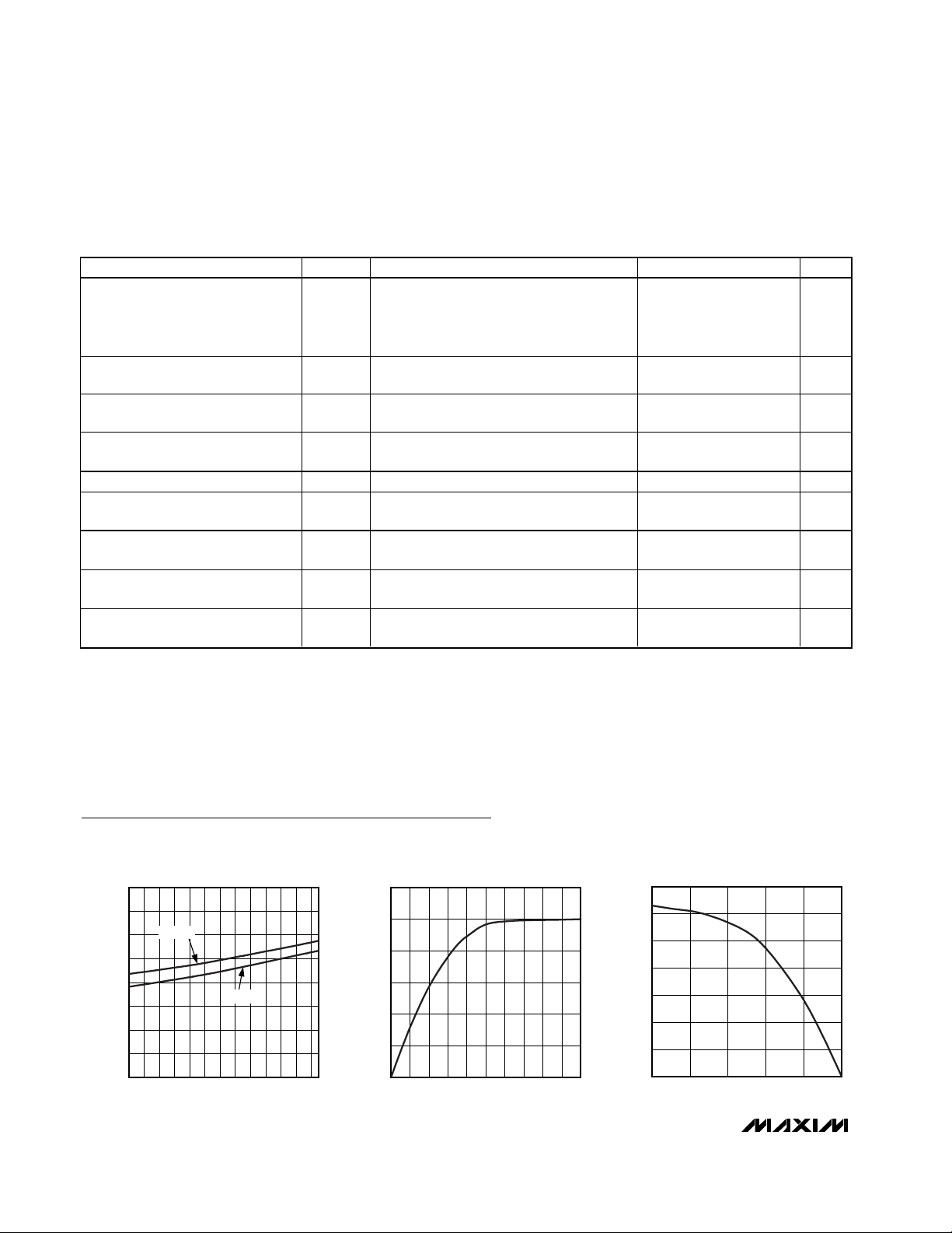
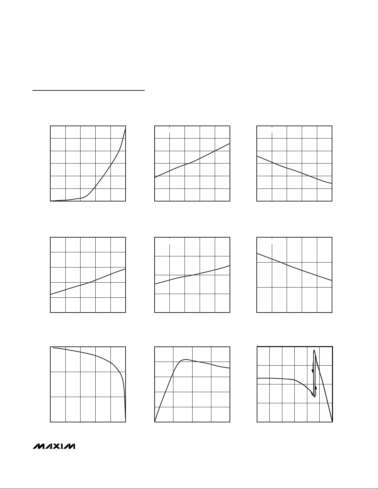
NO-LOAD SUPPLY CURRENT
vs. TEMPERATURE
MAX3465 toc01
TEMPERATURE (°C)
NO-LOAD SUPPLY CURRENT (mA)
6040-20 0 20
2.15
2.20
2.25
2.30
2.35
2.40
2.45
2.50
2.10
-40 80
DE = V
CC
DE = GND
OUTPUT CURRENT
vs. RECEIVER OUTPUT LOW VOLTAGE
MAX3465 toc02
OUTPUT LOW VOLTAGE (V)
OUTPUT CURRENT (mA)
4.54.03.53.02.52.01.51.00.5
10
20
30
40
50
60
0
0 5.0
OUTPUT CURRENT
vs. RECEIVER OUTPUT HIGH VOLTAGE
MAX3465 toc03
OUTPUT HIGH VOLTAGE (V)
OUTPUT CURRENT (mA)
4321
5
10
15
20
25
30
35
0
05
Typical Operating Characteristics
(VCC= +5V, TA = +25°C, unless otherwise noted.)
t
ZH (SHDN
800
t
ZL (SHDN
t
ZH (SHDN
t
ZL (SHDN
Page 5
MAX3465–MAX3469
+5V, Fail-Safe, 40Mbps, Profibus RS-485/
RS-422 Transceivers
_______________________________________________________________________________________ 5
Typical Operating Characteristics (continued)
(VCC= +5V, TA = +25°C, unless otherwise noted.)
SHUTDOWN SUPPLY CURRENT
vs. TEMPERATURE
300
250
200
150
100
SHUTDOWN SUPPLY CURRENT (nA)
50
0
-40 85
TEMPERATURE (°C)
603510-15
MAX3465 toc04
RECEIVER OUTPUT LOW VOLTAGE (mV)
RECEIVER PROPAGATION DELAY
vs. TEMPERATURE
20
18
16
14
PROPAGATION DELAY (ns)
12
MAX3465 toc07
PROPAGATION DELAY (ns)
RECEIVER OUTPUT LOW VOLTAGE
vs. TEMPERATURE
200
IO = -4mA
175
150
125
100
75
50
-40 85
TEMPERATURE (°C)
603510-15
DRIVER PROPAGATION DELAY
vs. TEMPERATURE
12
R
= 54Ω
DIFF
10
8
6
MAX3465 toc05
MAX3465 toc08
RECEIVER OUTPUT HIGH VOLTAGE
vs. TEMPERATURE
4.90
IO = 4mA
4.85
4.80
4.75
4.70
4.65
RECEIVER OUTPUT HIGH VOLTAGE (mV)
4.60
-40 85
TEMPERATURE (°C)
DRIVER DIFFERENTIAL OUTPUT VOLTAGE
vs. TEMPERATURE
3.5
R
= 54Ω
DIFF
3.0
2.5
OUTPUT VOLTAGE (V)
603510-15
MAX3465 toc06
MAX3465 toc09
10
-40 85
TEMPERATURE (°C)
603510-15
4
-40 85
DRIVER OUTPUT CURRENT
vs. DIFFERENTIAL OUTPUT VOLTAGE
100
MAX3465 toc10
10
1
OUTPUT CURRENT (mA)
0.1
05
DIFFERENTIAL OUTPUT VOLTAGE (V)
4321
vs. DRIVER OUTPUT LOW VOLTAGE
200
160
120
80
OUTPUT CURRENT (mA)
40
0
012
TEMPERATURE (°C)
OUTPUT CURRENT
OUTPUT LOW VOLTAGE (V)
603510-15
2.0
-40 85
TEMPERATURE (°C)
603510-15
OUTPUT CURRENT
vs. DRIVER OUTPUT HIGH VOLTAGE
-160
MAX3465 toc11
-120
-80
OUTPUT CURRENT (mA)
-40
0
963
-7 -1-5 -3 1 3 5
OUTPUT HIGH VOLTAGE (V)
MAX3465 toc12
Page 6

MAX3465–MAX3469
+5V, Fail-Safe, 40Mbps, Profibus RS-485/
RS-422 Transceivers
6 _______________________________________________________________________________________
Typical Operating Characteristics (continued)
(VCC= +5V, TA = +25°C, unless otherwise noted.)
DRIVER AND RECEIVER
PROPAGATION DELAYS
MAX3465 toc13
10ns/div
5V/div
5V/div
2V/div
Y, Z
DI
RO
R
DIFF
= 54Ω
DATA RATE = 20Mbps
ENABLE RESPONSE TIME
MAX3465 toc14
20ns/div
5V/div
1V/div
Y, Z
DE
R
DIFF
= 54Ω
EYE DIAGRAM
MAX3465 toc15
10ns/div
1V/div
Y, Z
R
DIFF
= 54Ω
DATA RATE = 20Mbps
Pin Description
FULL DUPLEX
MAX3465/
MAX3466
PIN
MAX3467
HALF
DUPLEX
MAX3468/
MAX3469
NAME FUNCTION
SHDN Shutdown. Drive SHDN high to enter low-power shutdown mode.
1 ——RO
221RE
3 — 2DE
4 — 3DI
5 3 4 GND Ground
6, 7 4 5 TXP
8 ——Y Noninverting Driver Output
95— Z Inverting Driver Output
10 6 — B Inverting Receiver Input
11 7 — A Noninverting Receiver Input
12 8 — RXP
13 ——V
CC
14 1 8 B Inverting Receiver Input and Inverting Driver Output
—— 7 A Noninverting Receiver Input and Noninverting Driver Output
——
Receiver Output. When RE is low and (A - B) ≥ -50mV, RO is high; if (A - B) ≤
-200mV, RO is low.
Receiver Output Enable. Drive RE low to enable RO; RO is high impedance
when RE is high. Drive RE high and DE low to enter low-power shutdown mode.
Driver Output Enable. Drive DE high to enable driver output. The driver
outputs are high impedance when DE is low. Drive RE high and DE low to
enter low-power shutdown mode.
Driver Input. With DE high, a low on DI forces the noninverting output low and
the inverting output high. Similarly, a high on DI forces the noninverting output
high and the inverting output low.
Transmitter Phase. Connect TXP to GND, or leave unconnected for normal
transmitter phase/polarity. Connect TXP to VCC to invert the transmitter
phase/polarity. TXP has an internal 15µA pulldown.
Receiver Phase. Connect RXP to GND, or leave unconnected for normal
receiver phase/polarity. Connect RXP to VCC to invert the receiver
phase/polarity. RXP has an internal 15µA pulldown.
Positive Supply: +4.75V ≤ VCC ≤ +5.25V. Bypass VCC to GND with a 0.1µF
capacitor.
Page 7

MAX3465–MAX3469
+5V, Fail-Safe, 40Mbps, Profibus RS-485/
RS-422 Transceivers
_______________________________________________________________________________________ 7
MAX3465/MAX3466
Function Tables
MAX3467
MAX3468/MAX3469
RE DE DI SHDN Z Y
X11001
X10010
0 0 X 0 High-Z High-Z
1 0 X X Shutdown
X X X 1 Shutdown
RE DE A - B SHDN RO
0X≥ -0.05V 0 1
0X≤ -0.2V 0 0
0 X Open/Shorted 0 1
1 1 X 0 High-Z
1 0 X X Shutdown
X X X 1 Shutdown
TRANSMITTING
INPUTS OUTPUTS
RECEIVING
INPUTS OUTPUT
INPUT OUTPUTS
DI Z Y
101
010
INPUTS OUTPUT
A - B RO
≥ -0.05V 1
≤ -0.2V 0
Open/Shorted 1
INPUTS OUTPUTS
RE DE DI B A
X11 0 1
X10 1 0
0 0 X High-Z High-Z
1 0 X Shutdown
TRANSMITTING
RECEIVING
TRANSMITTING
RECEIVING
INPUTS OUTPUT
RE DE A - B RO
0X ≥ -0.05V 1
0X ≤ -0.2V 0
0 X Open/Shorted 1
1 1 X High-Z
1 0 X Shutdown
Page 8

MAX3465–MAX3469
+5V, Fail-Safe, 40Mbps, Profibus RS-485/
RS-422 Transceivers
8 _______________________________________________________________________________________
Pin Configurations and Typical Operating Circuit
Figure 1. MAX3465/MAX3466 Pin Configuration and Typical Full-Duplex Operating Circuit
Figure 2. MAX3467 Pin Configuration and Typical Full-Duplex Operating Circuit
Figure 3. MAX3468/MAX3469 Pin Configuration and Typical Full-Duplex Operating Circuit
V
TOP VIEW
SHDN
GND
GND
1
2
RO
RE
DI
R
3
4
5
D
6
7
14
V
CC
13
RXP
12
A
11
BDE
10
Z
9
Y
TXP
8
TXP
RXP
DE
5
DI
2
RO
8
13
DIP/SO
CC
414
9ZY
D
R
3 GND
6, 7
RE
10
12
11
0.1µF
A
B
MAX3465
MAX3466
R
t
TOP VIEW
V
1
CC
0.1µF
MAX3467
V
RE
CC
R
t
GND
R
V
CC
RO
DI
D
DE
5ZY
6
A
8
R
7
B
V
GND
3
1
CC
RO
DI
R
2
3
D
4
8
A
7
B
6
Z
5
Y
DI
RO
D
2
DIP/SO
4 GND
TOP VIEW
R
1
RO
2
RE
3
DE
D
4
DI
8
RO
V
CC
7
B
RE
6
A
DE
5
GND
DI
R
1
2
3
D
4
V
8
CC
B
7
6
5
R
A
GND
DIP/SO
NOTE: PIN LABELS Y AND Z ON TIMING, TEST, AND WAVEFORM DIAGRAMS REFER TO PINS A AND B WHEN DE IS HIGH.
R
0.1µF
t
R
t
t
MAX3468
MAX3469
R
t
R
GND
DE
R
B
A
D
RE
RO
DI
D
DI
RO
Page 9

MAX3465–MAX3469
+5V, Fail-Safe, 40Mbps, Profibus RS-485/
RS-422 Transceivers
_______________________________________________________________________________________ 9
Detailed Description
The MAX3465–MAX3469 high-speed transceivers for
RS-485/RS-422 communication contain one driver and
one receiver. These devices feature true fail-safe circuitry, which guarantees a logic-high receiver output
when the receiver inputs are open or shorted, or when
they are connected to a terminated transmission line
with all drivers disabled (see the True Fail-Safe section). The MAX3465–MAX3469’s driver slew rates allow
transmit speeds up to 40Mbps.
The MAX3468 and MAX3469 are half-duplex transceivers, while the MAX3465, MAX3466, and MAX3467
are full-duplex transceivers. All of these parts operate
from a single +5V supply. Drivers are output short-circuit current limited. Thermal-shutdown circuitry protects
drivers against excessive power dissipation. When activated, the thermal-shutdown circuitry places the driver
outputs into a high-impedance state. The MAX3465
and MAX3468 devices have a hot-swap input structure
that prevents disturbances on the differential signal
lines when a circuit board is plugged into a hot backplane (see the Hot-Swap Capability section). All
devices have output levels that are compatible with
Profibus standards.
True Fail-Safe
The MAX3465–MAX3469 guarantee a logic-high receiver output when the receiver inputs are shorted or open,
or when they are connected to a terminated transmission line with all drivers disabled. This is done by setting the receiver threshold between -50mV and
-200mV. If the differential receiver input voltage (A - B)
is greater than or equal to -50mV, RO is logic high. If
A - B is less than or equal to -200mV, RO is logic low. In
the case of a terminated bus with all transmitters disabled, the receiver’s differential input voltage is pulled
to 0V by the termination. With the receiver thresholds of
the MAX3465–MAX3469, this results in a logic high with
a 50mV minimum noise margin. Unlike previous true
fail-safe devices, the -50mV to -200mV threshold complies with the ±200mV EIA/TIA-485 standard.
Hot-Swap Capability
Hot-Swap Inputs
When circuit boards are inserted into a “hot” or powered backplane, disturbances to the enable and differential receiver inputs can lead to data errors. Upon
initial circuit board insertion, the processor undergoes
its power-up sequence. During this period, the processor output drivers are high impedance and are unable
to drive the DE input of the MAX3465/MAX3468 to a
defined logic level. Leakage currents up to 10µA from the
high-impedance output could cause DE to drift to an
incorrect logic state. Additionally, parasitic circuit board
capacitance could cause coupling of V
CC
or GND to DE.
These factors could improperly enable the driver.
When VCCrises, an internal pulldown circuit holds DE
low for around 15µs. After the initial power-up
sequence, the pulldown circuit becomes transparent,
resetting the hot-swap-tolerable input.
Hot-Swap Input Circuitry
The MAX3465/MAX3468 enable inputs feature hot-swap
capability. At the input there are two NMOS devices, M1
and M2 (Figure 4). When VCCramps from 0, an internal
15µs timer turns on M2 and sets the SR latch, which
also turns on M1. Transistors M2, a 2mA current sink,
and M1, a 100µA current sink, pull DE to GND through a
5.6kΩ resistor. M2 is designed to pull DE to the disabled
state against an external parasitic capacitance up to
100pF that can drive DE high. After 15µs, the timer
deactivates M2 while M1 remains on, holding DE low
against three-state leakages that can drive DE high. M1
remains on until an external source overcomes the
required input current. At this time, the SR latch resets
and M1 turns off. When M1 turns off, DE reverts to a
standard, high-impedance CMOS input. Whenever V
CC
drops below 1V, the hot-swap input is reset.
For RE there is a complementary circuit employing two
PMOS devices pulling to VCC.
Figure 4. Simplified Structure of the Driver Enable Pin (DE)
V
CC
TIMER
EN
5.6kΩ
15µs
TIMER
2mA
100µA
M1 M2
DE
(HOT SWAP)
Page 10

MAX3465–MAX3469
+5V, Fail-Safe, 40Mbps, Profibus RS-485/
RS-422 Transceivers
10 ______________________________________________________________________________________
Figure 5. Driver DC Test Load
Figure 6. Driver Timing Test Circuit
Figure 7. Driver Propagation Delays
Figure 9. Driver Enable and Disable Times
Figure 10. Receiver Propagation Delays
Figure 11. Receiver Enable and Disable Times
Figure 8. Enable/Disable Timing Test Load
Y
R
V
OD
R
V
OC
Z
3V
DE
Y
DI
R
DIFF
V
ID
C
L
Z
O
f = 1MHz, tR ≤ 3ns, tF ≤ 3ns
t
PLH
V
= V (Y) - V (Z)
DIFF
90%
t
= | t
PLH
- t
SKEW
PHL
1.5V
t
PHL
90%
t
F
|
3V
DI
V
DIFF
1.5V
0V
Z
V
O
Y
1/2 V
V
O
0V
-V
10%
O
t
R
10%
1/2 V
3V
DE
0V
Y, Z
V
OL
Y, Z
0V
1.5V
t
, t
ZL(SHDN)
ZL
50%
OUTPUT NORMALLY LOW
OUTPUT NORMALLY HIGH
50%
t
, t
ZH(SHDN)
ZH
1.5V
t
LZ
V
+ 0.5V
OL
V
- 0.5V
OH
t
HZ
f = 1MHz, tR ≤ 3ns, tF ≤ 3ns
V
OH
-1V
RO
V
OL
A
1V
B
1.5V 1.5V
t
PHL
INPUT
OUTPUT
t
PLH
O
3V
RE
0V
V
CC
RO
RO
0V
1.5V
t
, t
ZL(SHDN)
1.5V
OUTPUT NORMALLY LOW
OUTPUT NORMALLY HIGH
1.5V
t
, t
ZH(SHDN)
1.5V
t
ZL
ZH
LZ
V
+ 0.5V
OL
- 0.5V
V
OH
t
HZ
V
CC
OUTPUT
R
L
S1
UNDER TEST
C
L
S2
Page 11

MAX3465–MAX3469
+5V, Fail-Safe, 40Mbps, Profibus RS-485/
RS-422 Transceivers
______________________________________________________________________________________ 11
Applications Information
128 Transceivers on the Bus
The standard RS-485 receiver input impedance is 12kΩ
(one unit load), and the standard driver can drive up to
32 unit loads. The MAX3465–MAX3469 family of transceivers has a 1/4-unit-load receiver input impedance
(48kΩ), allowing up to 128 transceivers to be connected in parallel on one communication line. Any combination of these devices and/or other RS-485 transceivers
with a total of 32 unit loads or less can be connected to
the line.
Low-Power Shutdown Mode
(Except MAX3467)
Low-power shutdown mode is initiated by bringing
SHDN high (MAX3465/MAX3466), or both RE high and
DE low. In shutdown, the devices typically draw only
1µA of supply current. RE and DE can be driven simultaneously; the devices are guaranteed not to enter shutdown if RE is high and DE is low for less than 50ns. If
the inputs are in this state for at least 800ns, the devices
are guaranteed to enter shutdown.
Driver Output Protection
Two mechanisms prevent excessive output current and
power dissipation caused by faults or by bus contention. The first, a foldback current limit on the output
stage, provides immediate protection against short circuits over the whole common-mode voltage range (see
the Typical Operating Characteristics). The second, a
thermal-shutdown circuit, forces the driver outputs into
a high-impedance state if the die temperature exceeds
+140°C.
Propagation Delay
Many digital encoding schemes depend on the difference
between the driver and receiver propagation delay times.
Typical propagation delays are shown in the Typical
Operating Characteristics. The difference in receiver delay
times, |t
PLH
- t
PHL
|, is a maximum of 2ns. The driver skew
time |t
PLH
- t
PHL
| is also a maximum of 2ns.
Typical Applications
The MAX3465–MAX3469 transceivers are designed for
bidirectional data communications on multipoint bus
transmission lines. Figures 13 and 14 show typical network applications circuits. To minimize reflections, the
line should be terminated at both ends in its characteristic impedance, and stub lengths off the main line
should be kept as short as possible.
Profibus Termination
The MAX3465–MAX3469 are designed for driving
Profibus termination networks. With a worst-case loading of two termination networks with 220Ω termination
impedance and 390Ω pullups and pulldowns, the drivers can drive V
A-B
> 2.1V output.
Chip Information
TRANSISTOR COUNT: 610
PROCESS: BiCMOS
Figure 12. Receiver Propagation Delay Test Circuit
Ordering Information (continued)
B
RECEIVER
ATE
V
ID
R
OUTPUT
A
PART TEMP RANGE PIN-PACKAGE
MAX3466CSD 0°C to +70°C 14 SO
MAX3466CPD 0°C to +70°C 14 Plastic DIP
MAX3466ESD -40°C to +85°C 14 SO
MAX3466EPD -40°C to +85°C 14 Plastic DIP
MAX3467CSA 0°C to +70°C 8 SO
MAX3467CPA 0°C to +70°C 8 Plastic DIP
MAX3467ESA -40°C to +85°C 8 SO
MAX3467EPA -40°C to +85°C 8 Plastic DIP
MAX3468CSA 0°C to +70°C 8 SO
MAX3468CPA 0°C to +70°C 8 Plastic DIP
MAX3468ESA -40°C to +85°C 8 SO
MAX3468EPA -40°C to +85°C 8 Plastic DIP
MAX3469CSA 0°C to +70°C 8 SO
MAX3469CPA 0°C to +70°C 8 Plastic DIP
MAX3469ESA -40°C to +85°C 8 SO
MAX3469EPA -40°C to +85°C 8 Plastic DIP
Page 12

MAX3465–MAX3469
+5V, Fail-Safe, 40Mbps, Profibus RS-485/
RS-422 Transceivers
12 ______________________________________________________________________________________
Figure 13. Typical Half-Duplex RS-485 Network
Figure 14. Typical Full-Duplex RS-485 Network
120Ω 120Ω
DI
D
B
B
D
DE
DE
RO
RE
R
MAX3468
A
D
MAX3469
(HALF-DUPLEX)
DI DE RO
A
RO
RE
DE
DI
R
D
120Ω
B
Z
120Ω
Y
AABAB
R
R
RE
D
DI DE RO
R
RE
120Ω
120Ω
Y
D
Z
B
R
A
DI
RO
RE
DI
DE
RE
RO
YZB A AB
D
DI DE RORE
NOTE: RE AND DE ON MAX3465/MAX3466/MAX3467 ONLY.
YZ
R
D
DI DE RORE
B
R
MAX3465
MAX3466
MAX3467
(FULL-DUPLEX)
Page 13

MAX3465–MAX3469
+5V, Fail-Safe, 40Mbps, Profibus RS-485/
RS-422 Transceivers
______________________________________________________________________________________ 13
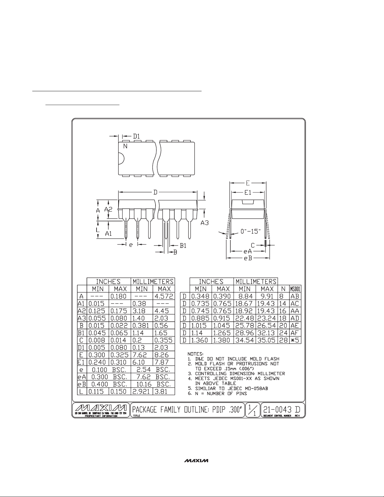
Package Information
(The package drawing(s) in this data sheet may not reflect the most current specifications. For the latest package outline information,
go to www.maxim-ic.com/packages
.)
N
1
TOP VIEW
D
e
FRONT VIEW
INCHES
DIM
MIN
0.053A
0.004
A1
0.014
B
0.007
C
e 0.050 BSC 1.27 BSC
0.150
HE
A
B
A1
C
L
E
H 0.2440.228 5.80 6.20
0.016L
VARIATIONS:
INCHES
MINDIM
D
0.189 0.197 AA5.004.80 8
0.337 0.344 AB8.758.55 14
D
0-8
SIDE VIEW
MAX
0.069
0.010
0.019
0.010
0.157
0.050
MAX
0.3940.386D
MILLIMETERS
MAX
MIN
1.35
1.75
0.10
0.25
0.35
0.49
0.19
0.25
3.80 4.00
0.40 1.27
MILLIMETERS
MAX
MIN
9.80 10.00
N MS012
16
AC
SOICN .EPS
PROPRIETARY INFORMATION
TITLE:
PACKAGE OUTLINE, .150" SOIC
REV.DOCUMENT CONTROL NO.APPROVAL
21-0041
1
B
1
Page 14
MAX3465–MAX3469
+5V, Fail-Safe, 40Mbps, Profibus RS-485/
RS-422 Transceivers
Maxim cannot assume responsibility for use of any circuitry other than circuitry entirely embodied in a Maxim product. No circuit patent licenses are
implied. Maxim reserves the right to change the circuitry and specifications without notice at any time.
14 ____________________Maxim Integrated Products, 120 San Gabriel Drive, Sunnyvale, CA 94086 408-737-7600
© 2003 Maxim Integrated Products Printed USA is a registered trademark of Maxim Integrated Products.
Package Information (continued)
(The package drawing(s) in this data sheet may not reflect the most current specifications. For the latest package outline information,
go to www.maxim-ic.com/packages
.)
PDIPN.EPS
 Loading...