

Page 1
General Description
The MAX3430 fault-protected RS-485 transceiver features
±80V protection from overvoltage signal faults on communication bus lines. Each device contains one driver and
one receiver, and the output pins can withstand faults,
with respect to ground, of up to ±80V. Even if the faults
occur when the transceiver is active, shut down, or powered off, the device will not be damaged. The MAX3430
operates from a 3.3V supply and features a slew-rate-limited driver that minimizes EMI and reduces reflections
caused by improperly terminated cables, allowing errorfree data transmission at data rates up to 250kbps. The
MAX3430 has a 1/4-unit-load receiver input impedance
allowing up to 128 transceivers on a single bus and features fail-safe circuitry, which guarantees a logic-high
receiver output when the receiver inputs are open.
Hot-swap circuitry eliminates false transitions on the
data cable during circuit initialization or connection to a
live backplane. Short-circuit current limiting and thermal-shutdown circuitry protect the driver against excessive power dissipation.
The MAX3430 is available in 8-pin SO and 8-pin PDIP
packages, and is specified over commercial and industrial temperature ranges.
Applications
RS-422/RS-485 Communications
Lighting Systems
Industrial-Control Local Area Networks
Profibus Applications
Multimaster RS-485 Networks
Features
♦ ±80V Fault Protection
♦ ±12kV ESD Protection
♦ +3.3V Operation
♦ Internal Slew-Rate Limiting
♦ 250kbps Data Rate
♦ Allows Up to 128 Transceivers on the Bus
♦ -7V to +12V Common-Mode Input Voltage Range
♦ True Fail-Safe Inputs
♦ Hot-Swap Input Structure on DE
♦ Available in 8-Pin SO and PDIP Packages
MAX3430
±80V Fault-Protected, Fail-Safe,
1/4-Unit Load, +3.3V RS-485 Transceiver
________________________________________________________________ Maxim Integrated Products 1
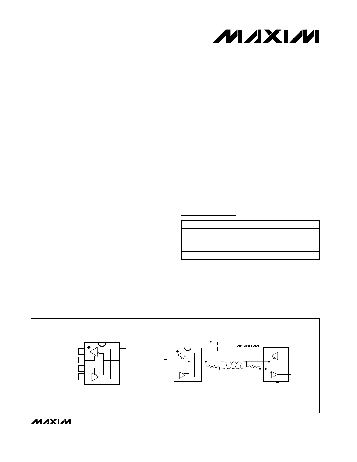
Pin Configuration and Typical Operating Circuit
Ordering Information
1
2
3
4
8
5
V
CC 0.1µF
GND
DI
DE
RE
RO
R
D
Rt
Rt
7
6
D
R
DE
RE
DI
RO
A
B
B
A
MAX3430
19-2756; Rev 0; 1/03
For pricing, delivery, and ordering information, please contact Maxim/Dallas Direct! at
1-888-629-4642, or visit Maxim’s website at www.maxim-ic.com.
PART TEMP RANGE PIN-PACKAGE
MAX3430CPD 0°C to +70°C 8 Plastic DIP
MAX3430CSD 0°C to +70°C 8 SO
MAX3430EPD -40°C to +85°C 8 Plastic DIP
MAX3430ESD -40°C to +85°C 8 SO
TOP VIEW
RO
RE
DE
DI
R
1
2
3
4
D
DIP/SO
V
8
CC
B
7
A
6
GND
5
Page 2
MAX3430
±80V Fault-Protected, Fail-Safe,
1/4-Unit Load, +3.3V RS-485 Transceiver
2 _______________________________________________________________________________________
ABSOLUTE MAXIMUM RATINGS
DC ELECTRICAL CHARACTERISTICS
(VCC= +3.3V ±10%, TA= T
MIN
to T
MAX
, unless otherwise noted. Typical values are at VCC= +3.3V and TA= +25°C.)
Stresses beyond those listed under “Absolute Maximum Ratings” may cause permanent damage to the device. These are stress ratings only, and functional
operation of the device at these or any other conditions beyond those indicated in the operational sections of the specifications is not implied. Exposure to
absolute maximum rating conditions for extended periods may affect device reliability.
(All voltages are referenced to GND.)
V
CC
........................................................................................+5V
RE, DE, DI...................................................-0.3V to (V
CC
+ 0.3V)
Driver Output Voltage (A, B) (Note 1) ..................................±80V
Receiver Input Voltage (A, B) (Note 1) ................................±80V
RO ..............................................................-0.3V to (V
CC
+ 0.3V)
Continuous Power Dissipation (T
A
= +70°C)
8-Pin SO (derate 5.88mW/°C above +70°C)................471mW
8-Pin Plastic DIP (derate 9.09mW/°C above +70°C) ...727mW
Operating Temperature Ranges
MAX3430C_ _ .....................................................0°C to +70°C
MAX3430E_ _ ..................................................-40°C to +85°C
Junction Temperature......................................................+150°C
Storage Temperature Range .............................-65°C to +150°C
Lead Temperature (soldering, 10s) .................................+300°C
Note 1: A, B must be terminated with 54Ω or 100Ω to guarantee ±80V fault protection.
DRIVER
Differential Driver Output V
Change in Magnitude of
Differential Output Voltage
Driver Common-Mode Output
Voltage
Change in Magnitude of
Common-Mode Voltage
DRIVER LOGIC
Driver Input High Voltage V
Driver Input Low Voltage V
Driver Input Current I
Driver Short-Circuit Output
Current
Driver Short-Circuit Foldback
Output Current
RECEIVER
Input Current (A, B) I
Receiver Differential Threshold
Voltage
Receiver Input Hysteresis ∆V
PARAMETER SYMBOL CONDITIONS MIN TYP MAX UNITS
OD
∆V
V
OC
∆V
IN
I
OSD
I
OSDF
A, B
V
Figure 1, RL = 100Ω 2.0 V
Figure 1, RL = 54Ω 1.5 V
Figure 1, RL = 100Ω or 54Ω (Note 2) 0.2 V
OD
Figure 1, RL = 100Ω or 54Ω V
Figure 1, RL = 100Ω or 54Ω (Note 2) 0.2 V
OC
DI 2.0 V
IH
DI 0.8 V
IL
DI ±1µA
0 ≤ V
-7V ≤ V
(V
-7V ≤ V
DE = GND, RE = GND, VIN = +12V 250
DE = GND, RE = GND, VIN = -7V -200
VIN = -80V to +80V -6 +6 mA
-7V ≤ VCM ≤ 12V -200 -50 mV
TH
VA + VB = 0 25 mV
TH
≤ 12V (Note 3) +250
OUT
≤ VCC (Note 3) -250
OUT
- 1V) ≤ V
CC
≤ 1V (Note 3) -10
OUT
CC
CC
/ 2 3 V
CC
≤ 12V (Note 3) +10
OUT
V
mA
mA
µA
Page 3
MAX3430
±80V Fault-Protected, Fail-Safe,
1/4-Unit Load, +3.3V RS-485 Transceiver
_______________________________________________________________________________________ 3
DC ELECTRICAL CHARACTERISTICS (continued)
(VCC= +3.3V ±10%, TA= T
MIN
to T
MAX
, unless otherwise noted. Typical values are at VCC= +3.3V and TA= +25°C.)
PROTECTION SPECIFICATIONS
(VCC= +3.3V ±10%, TA= T
MIN
to T
MAX
,
unless otherwise noted. Typical values are at V
CC
= +3.3V and TA= +25°C.)
RECEIVER LOGIC
RO Output High Voltage V
RO Output Low Voltage V
Three-State Output Current at
Receiver
Receiver Input Resistance R
Receiver Output Short-Circuit
Current
CONTROL
Control Input High Voltage V
Control Input Low Voltage V
Input Current DE Current Latch
During First DE Rising Edge
Input Current RE Current Latch
During First RE Rising Edge
PARAMETER SYMBOL CONDITIONS MIN TYP MAX UNITS
V
CC
0.6
I
OZR
I
OSR
OH
OL
IN
CIH
CIL
IO = -1.6mA
IO = 1mA 0.4 V
0 ≤ VO ≤ V
-7V ≤ VCM ≤ 12V 48 kΩ
0 ≤ VRO ≤ V
DE, RE 2.0 V
DE, RE 0.8 V
CC
CC
-
± 1µA
±95 mA
80 µA
80 µA
ESD Protection A, B Human Body Model ±12 kV
SUPPLY CURRENT
Supply Current I
Supply Current in Shutdown
Mode
PARAMETER SYMBOL CONDITIONS MIN TYP MAX UNITS
No load, RE = 0, DE = VCC, DI = 0 or V
CC
I
SHDN
No load, RE = VCC, DE = V
DI = 0 or V
RE = VCC, DE = 0 200 µA
CC
CC,
CC
3.5 10
3.0 8
V
mA
Page 4
MAX3430
±80V Fault-Protected, Fail-Safe,
1/4-Unit Load, +3.3V RS-485 Transceiver
4 _______________________________________________________________________________________
DRIVER SWITCHING CHARACTERISTICS
(VCC= +3.3V ±10%, TA= T
MIN
to T
MAX
, unless otherwise noted. Typical values are at VCC= +3.3V and TA= +25°C.)
)
)
RECEIVER SWITCHING CHARACTERISTICS
(VCC= +3.3V ±10%, TA= T
MIN
to T
MAX
, unless otherwise noted. Typical values are at VCC= +3.3V and TA= +25°C.)
)
)
Note 2: ∆VODand ∆VOCare the changes in VODand VOC, respectively, when the DI input changes state.
Note 3: The short-circuit output current applies to peak current just prior to foldback current limiting; the short-circuit foldback output
current applies during current limiting to allow a recovery from bus contention.
PARAMETER SYMBOL CONDITIONS MIN TYP MAX UNITS
Driver Propagation Delay
Driver Differential Output Rise or
Fall Time
Differential Driver Output Skew,
|t
- t
DPHL
|
DPLH
Maximum Data Rate 250 kbps
Driver Enable to Output Low t
Driver Disable Time from Output
Low
Driver Output Enable Time from
Shutdown
Driver Enable to Output High t
Driver Disable Time from Output
High
Driver Output Enable Time from
Shutdown
Driver Time to Shutdown t
t
DPLH
t
DPHL
t
DR, tDF
t
DSKEW
DZL
t
DLZ
t
DZL(SHDN
DZH
t
DHZ
t
DZH(SHDN
SHDN
Figures 2 and 3, RL = 54Ω, CL = 50pF
Figures 2 and 3, RL = 54Ω, CL = 50pF 250 1200 ns
Figures 2 and 3, RL = 54Ω, CL = 50pF 150 200 ns
Figure 4, CL = 50pF 5200 ns
Figure 4, CL = 50pF 1000 ns
Figure 4, CL = 50pF 8000 ns
Figure 5, CL = 50pF 5200 ns
Figure 5, CL = 50pF 1000 ns
Figure 5, CL = 50pF 8000 ns
700 1500
700 1500
1000 ns
ns
PARAMETER SYMBOL CONDITIONS MIN TYP MAX UNITS
Receiver Propagation Delay
Receiver Output Skew,
|t
- t
RPHL
|
RPLH
Receiver Enable to Output Low t
Receiver Enable to Output High t
Receiver Disable Time from Low t
Receiver Disable Time form High t
Receiver Output Enable Time
from Shutdown
Receiver Time to Shutdown t
t
RPLH
t
RPHL
t
SKEW
RZL
RZH
RLZ
RHZ
t
RZH(SHND
t
RZL(SHND
SHDN
Figure 6, C
Figure 6, C
Figure 7, R = 1kΩ, C
Figure 7, R = 1kΩ, C
Figure 7, R = 1kΩ, C
Figure 7, R = 1kΩ , CL = 20pF 80 ns
,
Figure 7, R = 1kΩ, CL = 20pF 5000 ns
= 20pF, V
L
= 20pF 40 ns
L
= 2V, VCM = 0
ID
= 20pF 80 ns
L
= 20pF 80 ns
L
= 20pF 80 ns
L
120
120
ns
1000 ns
Page 5

MAX3430
±80V Fault-Protected, Fail-Safe,
1/4-Unit Load, +3.3V RS-485 Transceiver
_______________________________________________________________________________________ 5
Typical Operating Characteristics
(VCC= +3.3V, TA= +25°C, unless otherwise noted.)
SUPPLY CURRENT
vs. TEMPERATURE
5
RE = 0
DE = V
CC
4
3
2
SUPPLY CURRENT (mA)
1
0
-40 0-20 20 40 60 80
TEMPERATURE (°C)
MAX3430 toc01
200
175
150
125
100
75
50
SHUTDOWN CURRENT (µA)
25
OUTPUT CURRENT
vs. RECEIVER OUTPUT HIGH VOLTAGE
18
15
12
9
6
OUTPUT CURRENT (mA)
3
3.30
3.25
MAX3430 toc04
3.20
3.15
3.10
OUTPUT HIGH VOLTAGE (V)
3.05
SHUTDOWN CURRENT
vs. TEMPERATURE
0
-40 0-20 20 40 60 80
TEMPERATURE (°C)
RECEIVER OUTPUT HIGH VOLTAGE
vs. TEMPERATURE
IO = -1.6mA
20
MAX3430 toc02
16
12
8
OUTPUT CURRENT (mA)
4
0
0 1.00.5 1.5 2.0 2.5 3.0 3.5
0.5
MAX3430 toc05
0.4
0.3
0.2
OUTPUT LOW VOLTAGE (V)
0.1
OUTPUT CURRENT
vs. RECEIVER OUTPUT LOW VOLTAGE
MAX3430 toc03
OUTPUT LOW VOLTAGE (V)
RECEIVER OUTPUT LOW VOLTAGE
vs. TEMPERATURE
IO = +1mA
MAX3430 toc06
0
0 1.00.5 1.5 2.0 2.5 3.0 3.5
OUTPUT HIGH VOLTAGE (V)
DRIVER OUTPUT CURRENT
vs. DIFFERENTIAL OUTPUT VOLTAGE
120
100
80
60
40
OUTPUT CURRENT (mA)
20
0
0 1.00.5 1.5 2.0 2.5 3.0 3.5
DIFFERENTIAL OUTPUT VOLTAGE (V)
3.00
-40 0-20 20 40 60 80
DRIVER DIFFERENTIAL OUTPUT VOLTAGE
3.5
3.0
MAX3430 toc07
2.5
2.0
1.5
1.0
0.5
DIFFERENTIAL OUTPUT VOLTAGE (V)
0
-40 0-20 20 40 60 80
TEMPERATURE (°C)
vs. TEMPERATURE
RL = 100Ω
RL = 54Ω
TEMPERATURE (°C)
MAX3430 toc08
0
-40 0-20 20 40 60 80
TEMPERATURE (°C)
A, B CURRENT
vs. A, B VOLTAGE (TO GROUND)
3
2
1
0
A, B CURRENT (mA)
-1
-2
-3
-80 -40-60 -20 0 20 40 60 80
RE = DE = GND
A, B VOLTAGE (V)
MAX3430 toc09
Page 6

MAX3430
±80V Fault-Protected, Fail-Safe,
1/4-Unit Load, +3.3V RS-485 Transceiver
6 _______________________________________________________________________________________
Figure 1. Driver DC Test Load
Figure 2. Driver Timing Test Circuit
Figure 3. Driver Propagation Delays
Figure 4. Driver Enable and Disable Times (t
DZL
, t
DLZ
,
t
DLZ(SHDN)
)
Figure 5. Driver Enable and Disable Times (t
DHZ
, t
DZH
, t
DZH(SHDN)
)
Test Circuits/Timing Diagrams
A
B
V
CC
DI
0
B
V
A
V
O
/2
V
CC
O
1/2 V
O
80%
20%
t
DR
V
OD
V
t
SKEW
t
OD
DPLH
= V (A) - V (B)
= |t
- t
DPLH
t
DPHL
DPHL
R
L
2
R
L
V
OC
2
3V
C
DE
A
DI
V
O
R
L
L
B
C
L
V
CC
= 500Ω
R
S1
1/2 V
0 OR +3V
O
GENERATOR
D
50Ω
80%
20%
t
DF
|
V
OUT
DE
CC
t
DZL
V
, t
OL
DZL(SHDN)
V
= (VOL + VCC)/2
OM
L
OUT
C
L
50pF
V
CC
VCC/2
t
DLZ
0
0.25V
S1
0 OR +3V
GENERATOR
50Ω
D
C
L
50pF
R
OUT
= 500Ω
L
DE
OUT
t
DZH
, t
DZH(SHDN)
V
OM
= (0 + VOH)/2
t
DHZ
VCC/2
0.25V
V
CC
0
V
OH
0
Page 7

MAX3430
±80V Fault-Protected, Fail-Safe,
1/4-Unit Load, +3.3V RS-485 Transceiver
_______________________________________________________________________________________ 7
Figure 6. Receiver Propagation Delays
Figure 7. Receiver Enable and Disable Times
Test Circuits/Timing Diagrams (continued)
V
ID
R
0
+1.5V
-1.5V
S3
GENERATOR
C
L
20pF
V
B
A
V
t
RPLH
OH
1.5V
V
OL
RO
R
C
20pF
1kΩ
L
R
50Ω
RO
ID
S1
S2
t
RPHL
V
CC
RE
t
, t
RZH
RZH(SHDN)
RO
RE
RO
0.25V
1.5V
t
RHZ
3V
0
V
OH
VOH/2
0
3V
0
V
OH
0
S1 OPEN
S2 CLOSED
S3 = +1.5V
S1 OPEN
S2 CLOSED
S3 = +1.5V
3V
0
V
CC
V
OL
3V
0
V
CC
V
OL
S1 CLOSED
S2 OPEN
S3 = -1.5V
S1 CLOSED
S2 OPEN
S3 = -1.5V
RE
t
, t
RZL
RO
RE
RO
1.5V
t
RLZ
0.25V
1.5V
RZL (SHDN)
(VOL + VCC)/2
Page 8

MAX3430
±80V Fault-Protected, Fail-Safe,
1/4-Unit Load, +3.3V RS-485 Transceiver
8 _______________________________________________________________________________________
Pin Description
Function Tables
Table 1. Transmitting
Table 2. Receiving
X = Don’t care.
X = Don’t care.
PIN NAME FUNCTION
1 RO Receiver Output
2 RE
3DE
4DI
5 GND Ground
6 A Noninverting Receiver Input/Driver Output
7 B Inverting Receiver Input/Driver Output
8VCCPositive Supply, VCC = +3.3V ±10%. Bypass V
INPUTS OUTPUTS
RE DE DI B A
X 1 1 0 1 Normal
X 1 0 1 0 Normal
0 0 X High-Z High-Z Normal
1 0 X High-Z High-Z Shutdown
Receiver Output Enable. RO is enabled when RE is low; RO is high impedance when RE is high. The
device enters a low-power shutdown mode if RE is high and DE is low.
Driver Output Enable. Driving DE high enables the driver outputs. Pulling DE low puts the driver
outputs in a high-impedance state. If RE is high and DE is low, the device enters a low-power
shutdown mode. If the driver outputs are enabled, the device functions as a line driver, and when
they are high impedance it functions as a line receiver if RE is low.
Driver Input. A logic low on DI forces output A low and output B high, while a logic high on DI forces
output A high and output B low.
to GND with a 0.1µF ceramic capacitor.
CC
MODE
RE DE (A - B) RO
00≥ -50mV 1 Normal
00≤ -200mV 0 Normal
00
1 0 X High-Z Shutdown
INPUTS OUTPUTS
Inputs
open
1 Normal
MODE
Page 9

MAX3430
±80V Fault-Protected, Fail-Safe,
1/4-Unit Load, +3.3V RS-485 Transceiver
_______________________________________________________________________________________ 9
Detailed Description
Driver
The driver accepts a single-ended, logic-level input
(DI) and transfers it to a differential, RS-485 level output
(A and B). Driving DE high enables the driver, while
pulling DE low places the driver outputs (A and B) into
a high-impedance state.
Receiver
The receiver accepts a differential, RS-485 level input
(A and B), and transfers it to a single-ended, logic-level
output (RO). Pulling RE low enables the receiver, while
driving RE high and DE low places the receiver inputs
(A and B) into a high-impedance state.
Low-Power Shutdown
Force DE low and RE high to shut down the MAX3430. A
time delay of 1µs prevents the device from accidentally
entering shutdown due to logic skews when switching
between transmit and receive modes. Holding DE low
and RE high for at least 1ms guarantees that the
MAX3430 enters shutdown. In shutdown, the device
consumes 100µA supply current.
±80V Fault Protection
The driver outputs/receiver inputs of RS-485 devices in
industrial network applications often experience voltage
faults resulting from transients that exceed the -7V to
+12V range specified in the EIA/TIA-485 standard. In
these applications, ordinary RS-485 devices (typical
absolute maximum ratings -8V to +12.5V) require costly
external protection devices. To reduce system complexity and the need for external protection, the driver
outputs/receiver inputs of the MAX3430 withstand voltage faults of up to ±80V with respect to ground without
damage (see the Absolute Maximum Ratings section,
Note 1). Protection is guaranteed regardless of whether
the device is active, shut down, or without power.
True Fail-Safe
The MAX3430 uses a -50mV to -200mV differential
input threshold to ensure true fail-safe receiver inputs.
This threshold guarantees the receiver outputs a logic
high for shorted, open, or idle data lines. The -50mV to
-200mV threshold complies with the ±200mV threshold
EIA/TIA-485 standard.
±12kV ESD Protection
As with all Maxim devices, ESD-protection structures
are incorporated on all pins to protect against ESD
encountered during handling and assembly. The
MAX3430 receiver inputs/driver outputs (A, B) have
extra protection against static electricity found in normal operation. Maxim’s engineers have developed
state-of-the-art structures to protect these pins against
±12kV ESD without damage. After an ESD event, the
MAX3430 continues working without latchup.
ESD protection can be tested in several ways. The
receiver inputs are characterized for protection up to
±12kV using the Human Body Model.
ESD Test Conditions
ESD performance depends on a number of conditions.
Contact Maxim for a reliability report that documents
test setup, methodology, and results.
Human Body Model
Figure 8a shows the Human Body Model, and Figure
8b shows the current waveform it generates when discharged into a low impedance. This model consists of
a 100pF capacitor charged to the ESD voltage of interest, which is then discharged into the device through a
1.5kΩ resistor.
Driver Output Protection
Two mechanisms prevent excessive output current and
power dissipation caused by faults or bus contention.
The first, a foldback current limit on the driver output
Figure 8a. Human Body ESD Test Model
Figure 8b. Human Body Model Current Waveform
R
C
1MΩ
CHARGE-CURRENT-
LIMIT RESISTOR
HIGH-
VOLTAGE
DC
SOURCE
C
s
100pF
R
D
1.5kΩ
DISCHARGE
RESISTANCE
STORAGE
CAPACITOR
DEVICE
UNDER
TEST
IP 100%
90%
AMPERES
36.8%
10%
0
0
t
RL
TIME
t
DL
CURRENT WAVEFORM
PEAK-TO-PEAK RINGING
I
r
(NOT DRAWN TO SCALE)
Page 10

MAX3430
±80V Fault-Protected, Fail-Safe,
1/4-Unit Load, +3.3V RS-485 Transceiver
10 ______________________________________________________________________________________
stage, provides immediate protection against short circuits over the whole common-mode voltage range. The
second, a thermal shutdown circuit, forces the driver
outputs into a high-impedance state if the die temperature exceeds +160°C. Normal operation resumes when
the die temperature cools by +140°C, resulting in a
pulsed output during continuous short-circuit conditions.
Hot-Swap Capability
Hot-Swap Inputs
Inserting circuit boards into a hot, or powered backplane
may cause voltage transients on DE, RE, and receiver
inputs A and B that can lead to data errors. For example,
upon initial circuit board insertion, the processor undergoes a power-up sequence. During this period, the highimpedance state of the output drivers makes them
unable to drive the MAX3430 enable inputs to a defined
logic level. Meanwhile, leakage currents of up to 10µA
from the high-impedance output, or capacitively coupled
noise from VCCor GND, could cause an input to drift to
an incorrect logic state. To prevent such a condition from
occurring, the MAX3430 features hot-swap input circuitry
on DE to safeguard against unwanted driver activation
during hot-swap situations. When VCCrises, an internal
pulldown circuit holds DE low for at least 10µs, and until
the current into DE exceeds 200µA. After the initial
power-up sequence, the pulldown circuit becomes
transparent, resetting the hot-swap tolerable input.
Hot-Swap Input Circuitry
At the driver enable input (DE), there are two NMOS
devices, M1 and M2 (Figure 9). When VCCramps from
0, an internal 15µs timer turns on M2 and sets the SR
latch, which also turns on M1. Transistors M2, a 2mA
current sink, and M1, a 100µA current sink, pull DE to
GND through a 5.6kΩ resistor. M2 pulls DE to the disabled state against an external parasitic capacitance
up to 100pF that may drive DE high. After 15µs, the
timer deactivates M2 while M1 remains on, holding DE
low against three-state leakage currents that may drive
DE high. M1 remains on until an external current source
overcomes the required input current. At this time, the
SR latch resets M1 and turns off. When M1 turns off, DE
reverts to a standard, high-impedance CMOS input.
Whenever VCCdrops below 1V, the input is reset.
Figure 9. Simplified Structure of the Driver Enable Pin (DE)
Figure 10. Typical RS-485 Network
V
CC
15µs
TIMER
TIMER
DE
5.6kΩ
100µA
M1 M2
DI
D
DE
RO
RE
2mA
120Ω 120Ω
B
A
R
BB
DE
(HOT SWAP)
B
D
AA
A
R
DE
DI
RO
RE
R
MAX3430
D
DE
DI RO DE
RE
D
DI
R
RO
RE
Page 11

MAX3430
±80V Fault-Protected, Fail-Safe,
1/4-Unit Load, +3.3V RS-485 Transceiver
______________________________________________________________________________________ 11
Applications Information
128 Transceivers on the Bus
The standard RS-485 receiver input impedance is 12kΩ
(one-unit load), and a standard driver can drive up to
32-unit loads. The MAX3430 transceiver 1/4-unit-load
receiver input impedance (48kΩ) allows up to 128
transceivers connected in parallel on one communication line. Connect any combination of these devices,
and/or other RS-485 devices, for a maximum of 32 unit
loads to the line.
RS-485 Applications
The MAX3430 transceiver provides bidirectional data
communications on multipoint bus transmission lines.
Figure 10 shows a typical network applications circuit.
The RS-485 standard covers line lengths up to 4000ft.
The signal line must be terminated at both ends in its
characteristic impedance, and stub lengths off the
main line kept as short as possible.
Chip Information
TRANSISTOR COUNT: 300
PROCESS: BiCMOS
Page 12

MAX3430
±80V Fault-Protected, Fail-Safe,
1/4-Unit Load, +3.3V RS-485 Transceiver
12 ______________________________________________________________________________________
Package Information
(The package drawing(s) in this data sheet may not reflect the most current specifications. For the latest package outline information,
go to www.maxim-ic.com/packages
.)
N
1
TOP VIEW
e
FRONT VIEW
INCHES
DIM
MIN
0.053A
0.004
A1
0.014
B
0.007
C
e 0.050 BSC 1.27 BSC
0.150
HE
D
A
B
A1
C
L
E
H 0.2440.228 5.80 6.20
0.016L
VARIATIONS:
INCHES
MINDIM
D
0.189 0.197 AA5.004.80 8
0.337 0.344 AB8.758.55 14
D
0-8
MAX
0.069
0.010
0.019
0.010
0.157
0.050
MAX
0.3940.386D
MILLIMETERS
MAX
MIN
1.35
1.75
0.10
0.25
0.35
0.49
0.19
0.25
3.80 4.00
0.40 1.27
MILLIMETERS
MAX
MIN
9.80 10.00
N MS012
16
AC
SOICN .EPS
SIDE VIEW
PROPRIETARY INFORMATION
TITLE:
PACKAGE OUTLINE, .150" SOIC
REV.DOCUMENT CONTROL NO.APPROVAL
21-0041
1
B
1
Page 13

MAX3430
±80V Fault-Protected, Fail-Safe,
1/4-Unit Load, +3.3V RS-485 Transceiver
Maxim cannot assume responsibility for use of any circuitry other than circuitry entirely embodied in a Maxim product. No circuit patent licenses are
implied. Maxim reserves the right to change the circuitry and specifications without notice at any time.
Maxim Integrated Products, 120 San Gabriel Drive, Sunnyvale, CA 94086 408-737-7600 ____________________ 13
© 2003 Maxim Integrated Products Printed USA is a registered trademark of Maxim Integrated Products.
Package Information (continued)
(The package drawing(s) in this data sheet may not reflect the most current specifications. For the latest package outline information,
go to www.maxim-ic.com/packages
.)
PDIPN.EPS
 Loading...