

Page 1
General Description
The MAX3420E contains the digital logic and analog
circuitry necessary to implement a full-speed USB
peripheral compliant to USB specification rev 2.0. A
built-in full-speed transceiver features ±15kV ESD protection and programmable USB connect and disconnect. An internal SIE (serial-interface engine) handles
low-level USB protocol details such as error checking
and bus retries. The MAX3420E operates using a register set accessed by an SPI interface that operates up to
26MHz. Any SPI master (microprocessor, ASIC, DSP,
etc.) can add USB functionality using the simple 3- or
4-wire SPI interface.
Internal level translators allow the SPI interface to run at
a system voltage between 1.71V and 3.6V. USB timed
operations are done inside the MAX3420E with interrupts provided at completion so an SPI master does not
need timers to meet USB timing requirements. The
MAX3420E includes four general-purpose inputs and
outputs so any microprocessor that uses I/O pins to
implement the SPI interface can reclaim the I/O pins
and gain additional ones.
The MAX3420E operates over the extended -40°C to
+85°C temperature range and is available in a 32-pin
TQFP package (7mm x 7mm) and a space-saving 24pin TQFN package (4mm x 4mm).
Applications
Features
♦ Microprocessor-Independent USB Solution
♦ Complies with USB Specification Revision 2.0
(Full-Speed Operation)
♦ Integrated Full-Speed USB Transceiver
♦ Firmware/Hardware Control of an Internal D+
Pullup Resistor
♦ Programmable 3- or 4-Wire 26MHz SPI Interface
♦ Level Translators and V
L
Input Allow Independent
System Interface Voltage
♦ Internal Comparator Detects V
BUS
for
Self-Powered Applications
♦ ESD Protection on D+, D-, and VBCOMP
♦ Interrupt Output Pin (Level or Programmable
Edge) Allows Polled or Interrupt-Driven SPI
Interface
♦ Intelligent USB Serial Interface Engine (SIE)
Automatically Handles USB Flow Control and
Double Buffering
Handles Low-Level USB Signaling Details
Contains Timers for USB Time-Sensitive
Operations So SPI Master Does Not Need to
Time Events
♦ Built-In Endpoint FIFOs:
EP0: CONTROL (64 Bytes)
EP1: OUT, Bulk or Interrupt, 2 x 64 Bytes
(Double-Buffered)
EP2: IN, Bulk or Interrupt, 2 x 64 Bytes
(Double-Buffered)
EP3: IN, Bulk or Interrupt (64 Bytes)
♦ Double-Buffered Data Endpoints Increase
Throughput by Allowing the SPI Master to
Transfer Data Concurrently with USB Transfers
Over the Same Endpoint
♦ SETUP Data Has Its Own 8-Byte FIFO, Simplifying
Firmware
♦ Four General-Purpose Inputs and Four General-
Purpose Outputs
♦ Space-Saving TQFP and TQFN Packages
MAX3420E
USB Peripheral Controller
with SPI Interface
________________________________________________________________ Maxim Integrated Products 1
19-3781; Rev 0; 8/05
For pricing, delivery, and ordering information, please contact Maxim/Dallas Direct! at
1-888-629-4642, or visit Maxim’s website at www.maxim-ic.com.
Cell Phones
PC Peripherals
Microprocessors and
DSPs
Custom USB Devices
Cameras
Desktop Routers
PLCs
Set-Top Boxes
PDAs
MP3 Players
Instrumentation
PART
TEMP RANGE
PINPACKAGE
PACKAGE
CODE
M AX 3420E E C J
32 TQFP
1.4m m
C 32- 1
M AX 3420E E TG*
24 TQFN
0.8m m
T2444- 4
Ordering Information
*Future product—contact factory for availability.
- 40°C to + 85°C
- 40°C to + 85°C
7m m x 7m m x
4m m x 4m m x
Page 2
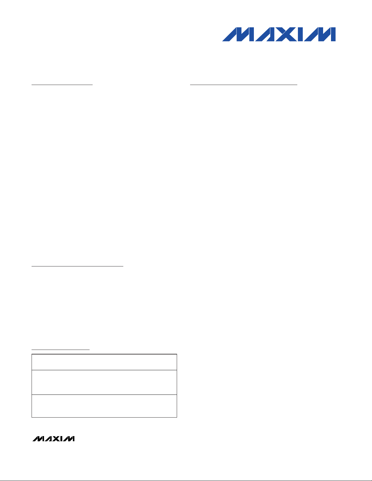
The MAX3420E connects to any microprocessor using
3 or 4 interface pins (Figure 1). On a simple microprocessor without SPI hardware, these can be bitbanged general-purpose I/O pins. Four GPIN and four
GPOUT pins on the MAX3420E more than replace the
µP pins necessary to implement the interface. Although
the MAX3420E SPI hardware includes separate data-in
(MOSI, (Master-Out, Slave-In)) and data-out (MISO,
(Master-In, Slave-Out)) pins, the SPI interface can also
be configured for the MOSI pin to carry bidirectional
data, saving an interface pin. This is referred to as halfduplex mode.
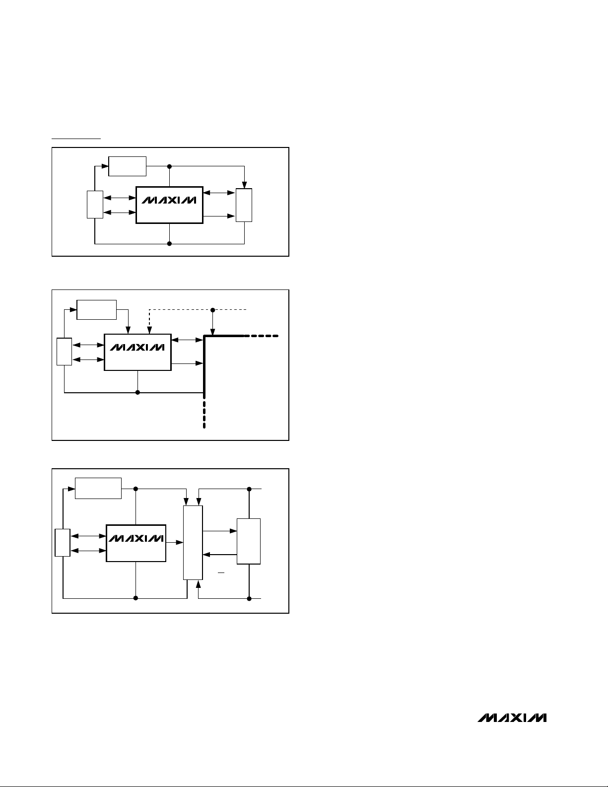
Two MAX3420E features make it easy to connect to
large, fast chips such as ASICs and DSPs (see Figure
2). First, the SPI interface can be clocked up to 26MHz.
Second, a VLpin and internal level translators allow
running the system interface at a lower voltage than the
3.3V required for VCC.
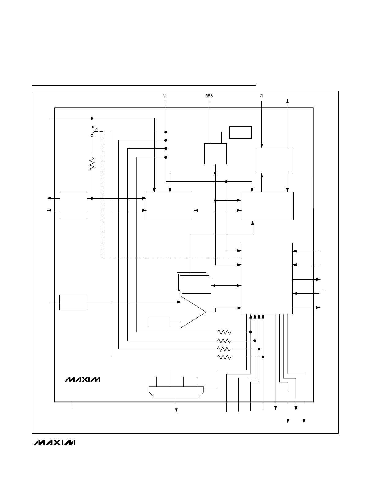
The MAX3420E provides an ideal method for electrically
isolating a USB interface (Figure 3). USB employs flow
control in which the MAX3420E automatically answers
host requests with a NAK handshake, until the microprocessor completes its data-transfer operations over
the SPI port. This means that the SPI interface can run
at any frequency up to 26MHz. Therefore, the designer
is free to choose the interface operating frequency and
to make opto-isolator choices optimized for cost or performance.
MAX3420E
USB Peripheral Controller
with SPI Interface
2 _______________________________________________________________________________________
Typical Application Circuits
3.3V
REGULATOR
SPI
3, 4
INT
USB
µ
P
MAX3420E
Figure 2. The MAX3420E Connected to a Large Chip
3.3V
REGULATOR
MISO
LOCAL
GND
LOCAL
POWER
INT
MAX3420E
SCLK
MOSI
SS
MICRO
ASIC
DSP
I
S
O
L
A
T
O
R
S
USB
Figure 3. Optical Isolation of USB Using the MAX3420E
Figure 1. The MAX3420E connects to any microprocessor
using 3 or 4 interface pins.
3.3V
REGULATOR
SPI
USB
MAX3420E
3, 4
INT
ASIC,
DSP,
ETC.
POWER RAIL
Page 3
MAX3420E
USB Peripheral Controller
with SPI Interface
_______________________________________________________________________________________ 3
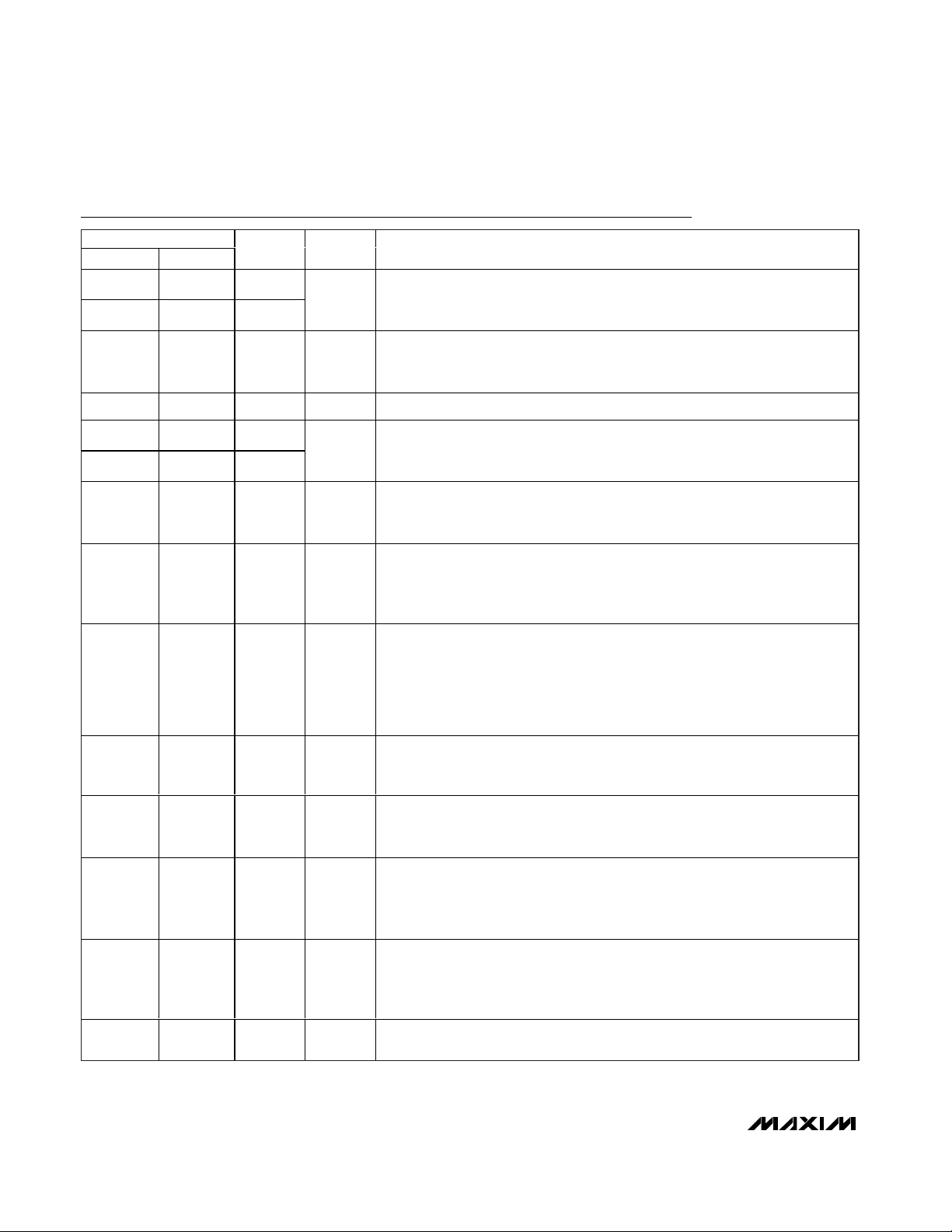
Functional Diagram
GPIN3
R
GPIN
1V–3V
VBCOMP
D-
D+
V
CC
GPIN2 GPIN1 GPIN0 GPOUT3
GPOUT2
GPOUT1
GPOUT0
VBUS
COMP
SS
MISO
SCLK
INT
SPI SLAVE
INTERFACE
USB SIE
(SERIAL-INTERFACE ENGINE)
FULL-SPEED
USB
TRANSCEIVER
RESET
LOGIC
1.5kΩ
INTERNAL
POR
RES
XIV
L
XO
POWER
DOWN
OSC
AND
PLL 4X
48MHZ
ESD
PROTECTION
ESD
PROTECTION
GPX
VBUS_DET
OPERATE
SOF
BUSACT
MUX
0123
MOSI
VBUS_DET
ENDPOINT
BUFFERS
MAX3420E
GND
Page 4
MAX3420E
USB Peripheral Controller
with SPI Interface
4 _______________________________________________________________________________________
Pin Description
PIN
TQFN TQFP
NAME
INPUT/
FUNCTION
11
22
G ener al - P ur p ose P ush- P ul l O utp uts. G P OU T3–G P OU T0 l og i c l evel s ar e r efer enced
to the vol tag e on V
L
. The S P I m aster contr ol s the G P OU T3–GP OU T0 states b y
w r i ti ng to b i t 3 thr oug h b i t 0 of the IOP IN S ( R20) r eg i ster .
3 3, 4 V
L
Input
Level-Translator Reference Voltage. Connect V
L
to the system’s 1.71V to 3.6V
logic-level power supply. Bypass V
L
to ground with a 0.1µF capacitor as close to
the V
L
pin as possible.
4, 14
GND Input Ground
57
68
Gener al - P ur p ose P ush- P ul l O utp uts. GP OU T3–GP O U T0 l og i c l evel s ar e r efer enced to
the vol tag e on V
L
. The S P I m aster contr ol s the GP O U T3–GP OU T0 states b y w r i ti ng to
b i t 3 thr oug h b i t 0 of the IOP IN S ( R20) r eg i ster .
710RES Input
Device Reset. Drive RES low to clear all of the internal registers except for
PINCTL (R17), USBCTL (R15), and SPI logic. See the Device Reset section for a
description of resets available on the MAX3420E.
811SCLK Input
SPI Serial-Clock Input. An external SPI master supplies this clock with frequencies
up to 26MHz. The logic level is referenced to the voltage on V
L
. Data is clocked
into the SPI slave interface on the positive edge of SCLK. Data is clocked out of
the SPI slave interface on the falling edge of SCLK.
912SS Input
SPI Slave-Select Input. The SS logic level is referenced to the voltage on V
L
.
When SS is driven high, the SPI slave interface is not selected and SCLK
transitions are ignored. An SPI transfer begins with a high-to-low SS transition and
ends with a low-to-high SS transition. The MAX3420E SS pin is sensitive to
undershoot. A 33pF capacitor should be connected from SS to ground to prevent
any noise spikes.*
10 13 MISO
SPI Serial-Data Output (Master-In, Slave-Out). MISO is a push-pull output. MISO is
tri-stated in half-duplex mode or when SS = 1. The MISO logic level is referenced
to the voltage on V
L
.
11 14 MOSI
Input or
Input/
SPI Serial-Data Input (Master-Out, Slave-In). The logic level on MOSI is
referenced to the voltage on V
L
. MOSI can also be configured as a bidirectional
MOSI/MISO input and output.
12 15 GPX
General-Purpose Multiplexed Output. The internal MAX3420E signal that appears
on GPX is programmable by writing to the GPXB and GPXA bits of the PINCTL
(R17) register. GPX indicates one of four signals: OPERATE (00, Default),
VBUS_DET (01), BUSACT (10), and SOF (11).
13 17 INT
Inter r up t Outp ut. In ed g e m od e, the l og i c l evel on IN T i s r efer enced to the vol tag e
on V L. In ed g e m od e , IN T i s a p ush- p ul l outp ut w i th p r og r am m ab l e p ol ar i ty. In l evel
m od e, IN T i s op en d r ai n and acti ve l ow . S et the IE b i t i n the C P U C TL ( R16) r eg i ster to
enab l e IN T.
15 20 D-
Input/
U S B D - S i g nal . C onnect D - to a U S B “B” connector thr ough a 33Ω ( ±1%) ser ies re si stor .
*33pF capacitor will not be required after redesign.
OUTPUT
GPOUT0
Output
GPOUT1
5, 6, 18, 19
GPOUT2
GPOUT3
Output
Output
Output
Output
Output
Output
Page 5
Register Description
The SPI master controls the MAX3420E by reading and
writing 21 registers (Table 1). For a complete description of register contents, please refer to the “MAX3420E
Programming Guide.” A register access consists of the
SPI master first writing an SPI command byte, followed
by reading or writing the contents of the addressed
register. All SPI transfers are MSB (most significant bit)
first. The command byte contains the register address,
a direction bit (Read = 0, Write = 1), and the ACKSTAT
bit (Figure 4). The SPI master addresses the
MAX3420E registers by writing the binary value of the
register number in the Reg4 through Reg0 bits of the
command byte. For example, to access the IOPINS
(R20) register, the Reg4 through Reg0 bits would be as
follows: Reg4 = 1, Reg3 = 0, Reg2 = 1, Reg1 = 0, Reg0
= 0. The DIR (direction) bit determines the direction for
the data transfer. DIR = 1 means the data byte(s) will
be written to the register, and DIR = 0 means the data
byte(s) will be read from the register. The ACKSTAT bit
sets the ACKSTAT bit in the EPSTALLS (R9) register.
The SPI master sets this bit to indicate that it has finished servicing a CONTROL transfer. Since the bit is
frequently used, having it in the SPI command byte
improves firmware efficiency. In SPI full-duplex mode,
the MAX3420E clocks out eight USB status bits as the
command byte is clocked in (Figure 5). In half-duplex
MAX3420E
USB Peripheral Controller
with SPI Interface
_______________________________________________________________________________________ 5
Pin Description (continued)
PIN
TQFN TQFP
NAME
INPUT/
FUNCTION
16 21 D+
Input/
USB D+ Signal. Connect D+ to a USB “B” connector through a 33Ω (±1%)
series resistor. The 1.5kΩ D+ pullup resistor is internal to the device.
17 22, 23 V
CC
Input
USB Transceiver Power-Supply Input. Connect V
CC
to a positive 3.3V power
supply. Bypass V
CC
to ground with a 1.0µF ceramic capacitor as close to the
V
CC
pin as possible.
18 24
Input
V
BUS
Comparator Input. VBCOMP is internally connected to a voltage
comparator to allow the SPI master to detect (through an interrupt or checking
a register bit) the presence or loss of power on V
BUS
. Bypass VBCOMP to
ground with a 1.0µF ceramic capacitor.
19 26 XI Input
Crystal Oscillator Input. Connect XI to one side of a parallel resonant 12MHz
(±0.25%) crystal and a capacitor to GND. XI can also be driven by an external
clock referenced to V
CC
.
20 27 XO
Crystal Oscillator Output. Connect XO to the other side of a parallel resonant
12MHz (±0.25%) crystal and a capacitor to GND. Leave XO unconnected if XI
is driven with an external source.
21 29 GPIN0
22 30 GPIN1
23 31 GPIN2
24 32 GPIN3
Input
General-Purpose Inputs. GPIN3–GPIN0 are connected to V
L
with internal
pullup resistors. GPIN3–GPIN0 logic levels are referenced to the voltage on V
L
.
The SPI master samples GPIN3–GPIN0 states by reading bit 7 through bit 4 of
the IOPINS (R20) register. Writing to these bits has no effect.
—
N.C. — No Internal Connection
EP — GND Input Exposed Paddle on the Bottom of the TQFN Package. Connect EP to GND.
Figure 4. SPI Command Byte
b7 b6 b5 b4 b3 b2 b1 b0
Reg4 Reg3 Reg2 Reg1 Reg0 0 DIR ACKSTAT
Figure 5. USB Status Bits Clocked Out as First Byte of Every Transfer (Full-Duplex Mode Only)
b7 b6 b5 b4 b3 b2 b1 b0
SUSPIRQ URESIRQ
IN0BAVIRQ
9, 16, 25, 28
VBCOMP
OUTPUT
Output
Output
SUDAVIRQ IN3BAVIRQ IN2BAVIRQ OUT1DAVIRQ OUT0DAVIRQ
Page 6
MAX3420E
mode, these status bits are accessed in the normal
way, as register bits.
The first five registers (R0–R4) access endpoint FIFOs.
To access a FIFO, an initial command byte sets the
register address and then consecutive reads or writes
keep the same register address to access subsequent
FIFO bytes.
The remaining registers (R5–R20) control the operation
of the MAX3420E. Once a register address above R4 is
set in the command byte, successive byte reads or
writes in the same SPI access cycle (SS low) increment
the register address after every byte read or written. This
incrementing operation continues until R20 is accessed.
Subsequent byte reads or writes continue to access
R20. Note that this auto-incrementing action stops with
the next SPI cycle, which establishes a new register
address. Addressing beyond R20 is ignored.
USB Peripheral Controller
with SPI Interface
6 _______________________________________________________________________________________
Table 1. MAX3420E Register Map
R EG
NAME b 7 b 6 b 5 b 4 b 3 b 2 b 1 b 0
a c c
R0
EP0 F IF O b 7b 6b 5b 4b 3b 2b 1b 0
RS C
R1
b 7b 6b 5b 4b 3b 2b 1b 0
RS C
R2
EP2 IN F IF O b 7b 6b 5b 4b 3b 2b 1b 0
RS C
R3
EP3 IN F IF O b 7b 6b 5b 4b 3b 2b 1b 0
RS C
R4
SU D F IF O b 7b 6b 5b 4b 3b 2b 1b 0
RS C
R5
EP0 B C 0b 6b 5b 4b 3b 2b 1b 0
RS C
R6
EP1 O U T B C 0b 6b 5b 4b 3b 2b 1b 0
RS C
R7
EP2 IN B C 0b 6b 5b 4b 3b 2b 1b 0
RS C
R8
EP3 IN B C 0b 6b 5b 4b 3b 2b 1b 0
RS C
R9
EPST A L L S 0
RS C
R10
C L R T O G S
00
RS C
R11
EPI R Q 00
RC
R12
EPI EN 00
RS C
R13
U SB IR Q
RC
R14
U SB IEN
RS C
R15
U SB C T L
S IG RWU 0 0
RS C
R16
C PU C T L 000 00 0 0 IE
RS C
R17
PIN C T L
P OS IN TGP X BGP X A
RS C
R18
R EVISIO N 000 00 0 1 0
R
R19
F N A D D R 0b 6b 5b 4b 3b 2b 1b 0
R
R20
IO PIN S GP IN 3
GP IN 1GP IN 0
GP O U T2 GP O U T1
RS C
Note: The acc (access) column indicates how the SPI Master can access the register.
R = Read, RC = Read or Clear, RSC = Read, Set, or Clear.
Writing to an R register (Read-Only) has no effect.
Writing a 1 to an RC bit (Read or Clear) clears the bit.
Writing a zero to an RC bit has no effect.
EP1 O U T F IF O
AC KS TAT S TLS TAT S TLE P 3IN S TLE P 2IN S TLE P 1OU TS TLE P 0OU TS TLE P 0IN
E P 3D IS AB E P 2D IS AB E P 1D IS AB C TG E P 3IN C TG E P 2IN C TG E P 1OU T
S U D AV IRQ IN 3BAV IRQ IN 2BAV IRQ OU T1D AV IRQ OU T0D AV IRQ IN 0BAV IRQ
S U D AV IE IN 3BAV IE IN 2BAV IE OU T1D AV IE OU T0D AV IE IN 0BAV IE
U RE S D N IRQ V BU S IRQ N OV BU S IRQ S U S P IRQ U RE S IRQ BU S AC TIRQ RWU D N IRQ OS C OKIRQ
U RE S D N IE V BU S IE N OV BU S IE S U S P IE U RE S IE BU S AC TIE RWU D N IE OS C OKIE
H OS C S TE N V BG ATE C H IP RE S P WRD OWN C ON N E C T
E P 3IN AK E P 2IN AK E P 0IN AK FD U P S P IIN TLE V E L
GP IN 2
GP O U T3
GP O U T0
Page 7
MAX3420E
USB Peripheral Controller
with SPI Interface
_______________________________________________________________________________________ 7
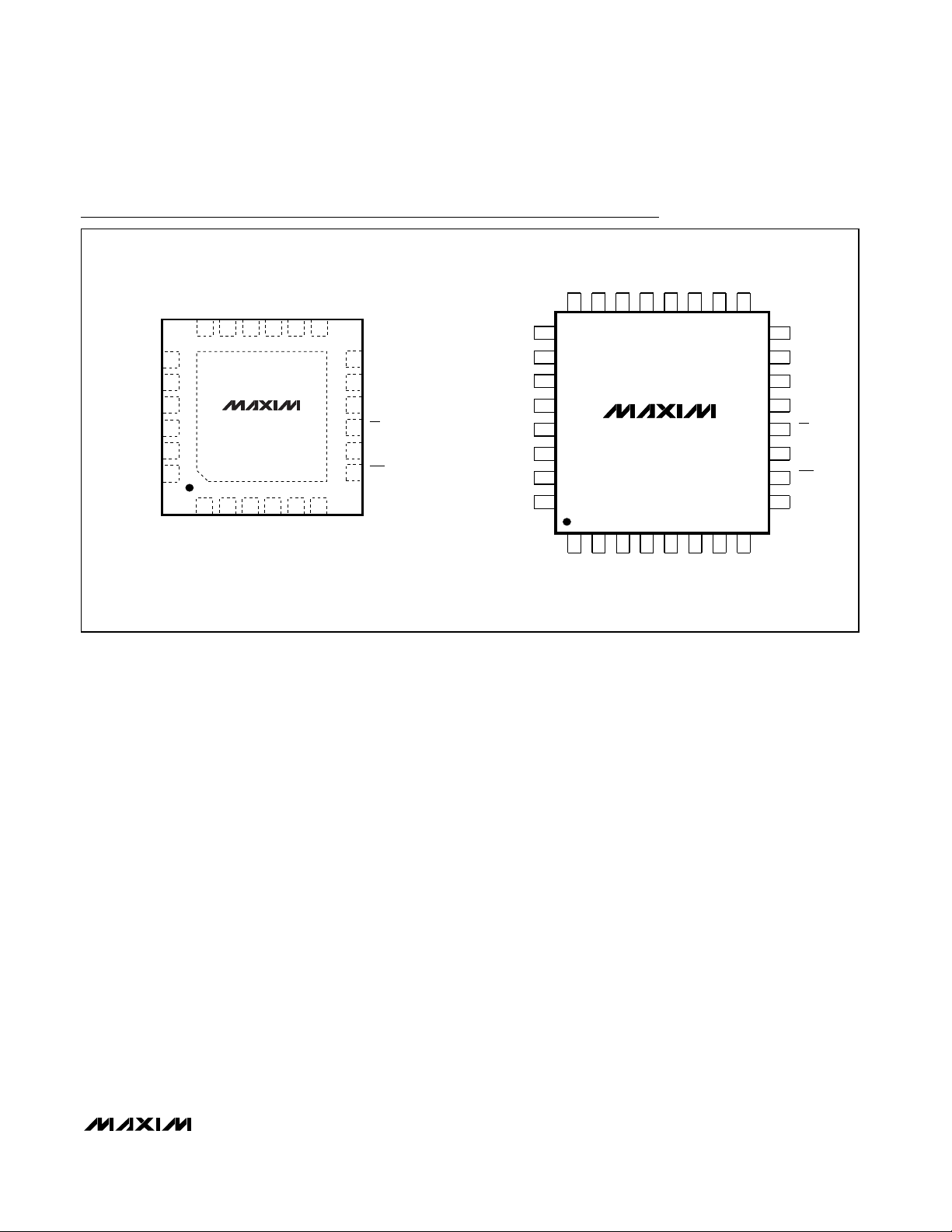
TQFN
MAX3420E
*EP
1234
7
8
9
10
11
* EXPOSED PADDLE CONNECTED TO GROUND
12
24
23
22
21
20
19
56
18 17 16 15 14 13
GPOUT0
V
L
GPOUT1
GPOUT3
SCLK
RES
MISO
MOSI
GPX
GPIN3
GPIN2
GPIN0
XO
XI
GPOUT2
GND
VBCOMP
D+
V
CC
D-
INT
GND
GPIN1
TOP VIEW
MAX3420E
TQFP
TOP VIEW
32
28
29
30
31
25
26
27
GPIN2
GPIN1
GPIN0
N.C.
GPIN3
XO
XI
N.C.
10
13
15
14
16
11
12
9
N.C.
SCLK
RES
MISO
SS
GPX
MOSI
N.C.
17181920212223
V
CC
24
VBCOMP
V
CC
D+
D-
GND
GND
INT
2
3
4
5
6
7
8
GPOUT3
GPOUT2
GND
GND
V
LVL
GPOUT1
1
GPOUT0
SS
Pin Configurations
Page 8

MAX3420E
USB Peripheral Controller
with SPI Interface
8 _______________________________________________________________________________________
ABSOLUTE MAXIMUM RATINGS
ELECTRICAL CHARACTERISTICS
(VCC= +3V to +3.6V, VL= +1.71V to +3.6V, TA= T
MIN
to T
MAX
, unless otherwise noted. Typical values are at VCC= +3.3V, VL=
+2.5V, T
A
= +25°C.) (Note 1)
Stresses beyond those listed under “Absolute Maximum Ratings” may cause permanent damage to the device. These are stress ratings only, and functional
operation of the device at these or any other conditions beyond those indicated in the operational sections of the specifications is not implied. Exposure to
absolute maximum rating conditions for extended periods may affect device reliability.
(All voltages referenced to GND, unless otherwise noted.)
V
CC
......................................................................... -0.3V to +4V
V
L
.............................................................................-0.3V to +4V
VBCOMP .................................................................-0.3V to +6V
D+, D-, XI, XO ............................................-0.3V to (V
CC
+ 0.3V)
SCLK, MOSI, MISO, SS, RES, GPOUT3–GPOUT0,
GPIN3–GPIN0, GPX, INT ..........................-0.3V to (V
L
+ 0.3V)
Continuous Power Dissipation (T
A
= +70°C)
24-Pin TQFN (derate 20.8mW/°C above +70°C) .......1667mW
32-Pin TQFP (derate 20.7mW/°C above +70°C)........1653mW
Operating Temperature Range ...........................-40°C to +85°C
Junction Temperature......................................................+150°C
Storage Temperature Range .............................-65°C to +150°C
Lead Temperature (soldering, 10s) .................................+300°C
PARAMETER
CONDITIONS
UNITS
DC CHARACTERISTICS
Supply Voltage V
CC
V
CC
3.0 3.3 3.6 V
Logic-Core Supply and LogicInterface Voltage V
L
V
L
V
VCC Supply Current I
CC
Continuously transmitting on D+ and D- at
12Mbps, C
L
= 50pF on D+ and D- to GND,
CONNECT = 0
15 30 mA
VL Supply Current I
L
SCLK toggling at 20MHz, SS = low,
GPIN3–GPIN0 = 0
620mA
V
CC
Supply Current During Idle I
CCID
D+ = high, D- = low 1.5 5 mA
VCC Suspend Supply Current I
CCSUS
CONNECT = 0, PWRDOWN = 1 33
µA
V L S usp end S up p l y C urr ent I
LSUS
CONNECT = 0, PWRDOWN = 1 ( N ote 6) 2.0 10 mA
LOGIC-SIDE I/O
I
LOAD
= +5mA, VL < 2.5V
MISO, GPOUT3–GPOUT0, GPX,
INT Output-High Voltage
V
OH
I
LOAD
= +10mA, VL ≥ 2.5V
V
I
LOAD
= -20mA, VL < 2.5V 0.6
MISO, GPOUT3–GPOUT0, GPX,
INT Output-Low Voltage
V
OL
I
LOAD
= -20mA, VL ≥ 2.5V 0.4
V
SCLK, MOSI, GPIN3–GPIN0, SS,
RES Input-High Voltage
V
IH
V
SCLK, MOSI, GPIN3-GPIN0, SS,
RES Input-Low Voltage
V
IL
0.4 V
SCLK, MOSI, SS, RES Input
Leakage Current
I
IL
1µA
GP IN 3–GP IN 0 P ul l up Resi stor to V
L
R
GPIN
10 20 30 kΩ
TRANSCEIVER SPECIFICATIONS
Differential-Receiver Input
Sensitivity
|V
D+
- VD-| 0.2 V
Differential-Receiver CommonMode Voltage
0.8 2.5 V
SYMBOL
MIN TYP MAX
1.71 3.60
V L - 0.45
V L - 0.4
2/3 x V
L
100
Page 9

MAX3420E
USB Peripheral Controller
with SPI Interface
_______________________________________________________________________________________ 9
ELECTRICAL CHARACTERISTICS (continued)
(VCC= +3V to +3.6V, VL= +1.71V to +3.6V, TA= T
MIN
to T
MAX
, unless otherwise noted. Typical values are at VCC= +3.3V, VL=
+2.5V, T
A
= +25°C.) (Note 1)
PARAMETER
CONDITIONS
UNITS
Single-Ended Receiver Input-Low
Voltage
V
IL
0.8 V
Single-Ended Receiver InputHigh Voltage
V
IH
2.0 V
Single-Ended Receiver
Hysteresis Voltage
0.2 V
D+, D- Input Impedance 300 kΩ
D+, D- Output-Low Voltage V
OL
RL = 1.5kΩ from D+ to 3.6V 0.3 V
D+, D- Output-High Voltage V
OH
RL = 15kΩ from D+ and D- to GND 2.8 3.6 V
Driver Output Impedance
Excluding External Resistor
(Note 2) 2 7 11 Ω
D+ Pullup Resistor R
EXT
= 33Ω
1.5
kΩ
ESD PROTECTION (D+, D-, VBCOMP)
Human Body Model
1µF ceramic capacitors from VBCOMP and
V
CC
to GND
kV
IEC61000-4-2 Air Discharge
1µF ceramic capacitors from VBCOMP and
V
CC
to GND
kV
IEC61000-4-2 Contact Discharge
1µF ceramic capacitors from VBCOMP and
V
CC
to GND
±8 kV
THERMAL SHUTDOWN
Thermal-Shutdown Low-to-High
°C
Thermal-Shutdown High-to-Low
°C
CRYSTAL OSCILLATOR SPECIFICATIONS (XI, XO)
XI Input High Voltage
V
XI Input Low Voltage 0.4 V
XI Input Current 10 µA
XI, XO Input Capacitance 3pF
VBCOMP COMPARATOR SPECIFICATIONS
VBCOMP Comparator Threshold
V
TH
1.0 2.0 3.0 V
VBCOMP Comparator Hysteresis
V
HYS
mV
VBCOMP Comparator Input
Impedance
R
IN
100 kΩ
SYMBOL
MIN TYP MAX
1.425
±15
2/3 x V
±12
+160
+140
C C
375
1.575
V
CC
Page 10

MAX3420E
USB Peripheral Controller
with SPI Interface
10 ______________________________________________________________________________________
Note 1: Parameters are 100% production tested at TA= +25°C, and guaranteed by correlation over temperature.
Note 2: Design guaranteed by bench testing. Limits are not production tested.
Note 3: At V
L
= 1.71V to 2.5V, derate all of the SPI timing characteristics by 50%. Not production tested.
Note 4: The minimum period is derived from SPI timing parameters.
Note 5: Time-to-exit suspend is dependent on the crystal used.
Note 6: Redesign in progress to meet USB specification.
PARAMETER
SYMBOL
CONDITIONS
MIN
TYP
MAX
UNITS
TIMING CHARACTERISTICS
(V
CC
= +3V to +3.6V, VL= +1.71V to +3.6V, TA= T
MIN
to T
MAX
, unless otherwise noted. Typical values are at VCC= +3.3V, VL=
+2.5V, T
A
= +25°C.) (Note 1)
*33pF capacitor will not be required after redesign.
PARAMETER SYMBOL CONDITIONS MIN TYP MAX UNITS
USB TRANSMITTER TIMING CHARACTERISTICS
D+, D- Rise Time t
D+, D- Fall Time t
Rise-/Fall-Time Matching CL = 50pF, Figures 6 and 7 (Note 2) 90 110 %
Output-Signal Crossover Voltage CL = 50pF, Figures 6 and 7 (Note 2) 1.3 2.0 V
SPI BUS TIMING CHARACTERISTICS (VL = 2.5V, C SS = 33pF*) (Figures 8 and 9) (Note 3)
S eri al C l ock ( SC LK) P eri od ( N ote 4) t
SCLK Pulse-Width High t
SCLK Pulse-Width Low t
SS Fall-to-MISO Valid t
SS Leading Time Before the First
SCLK Edge
SS Trailing Time After the Last
SCLK Edge
Data-In Setup Time t
Data-In Hold Time t
SS Pulse High t
SCLK Fall-to-MISO Propagation
Delay
SCLK Fall-to-MOSI Propagation
Delay
SCLK Rise-to-MOSI Drive t
SS High-to-MOSI High
Impedance
SUSPEND TIMING CHARACTERISTICS
Time-to-Enter Suspend PWRDOWN = 1 to oscillator stop 5 µs
Time-to-Exit Suspend PWRDOWN = 1 to 0 to OSCOKIRQ (Note 5) 3 ms
RISE
FALL
CP
CH
CL
CSS
t
L
t
T
DS
DH
CSW
t
DO
t
DI
ON
t
OFF
CL = 50pF, Figures 6 and 7 4 20 ns
CL = 50pF, Figures 6 and 7 4 20 ns
VL = 1.71V 77.0
VL = 2.5V 38.4
17 ns
17 ns
20 ns
30 ns
30 ns
5ns
10 ns
200 ns
14.2 ns
14.2 ns
3.5 ns
20 ns
ns
Page 11

MAX3420E
USB Peripheral Controller
with SPI Interface
______________________________________________________________________________________ 11
Test Circuits and Timing Diagrams
Figure 6. Rise and Fall Times
V
OL
V
OH
t
RISE
t
FALL
90%
10%
Figure 7. Load for D+/D- AC Measurements
MAX3420E
D+ OR D-
TEST
POINT
33Ω
15kΩ
C
L
Figure 9. SPI Bus Timing Diagram (Half-Duplex Mode, SPI Mode (0,0))
SCLK
MOSI
MISO
NOTES:
1) DURING THE FIRST 8 CLOCKS CYCLES, THE MOSI PIN IS HIGH IMPEDANCE AND THE SPI MASTER DRIVES DATA ONTO THE MOSI PIN. SETUP AND HOLD TIMES ARE THE SAME AS
FOR FULL-DUPLEX MODE.
2) FOR SPI WRITE CYCLES, THE MOSI PIN CONTINUES TO BE HIGH IMPEDANCE AND THE EXTERNAL MASTER CONTINUES TO DRIVE MOSI.
3) FOR SPI READ CYCLES, AFTER THE 8TH CLOCK-RISING EDGE, THE MAX3420E STARTS DRIVING THE MOSI PIN AFTER TIME t
ON
. THE EXTERNAL MASTER MUST TURN
OFF ITS DRIVER TO THE MOSI PIN BEFORE t
ON
TO AVOID CONTENTION. PROPAGATION DELAYS ARE THE SAME AS FOR THE MOSI PIN IN FULL-DUPLEX MODE.
t
DS
t
DH
t
CLtCH
t
DI
t
OFF
t
T
SS
HI-Z
HI-Z
HI-Z
8
1
2
9
10 16
t
L
t
CSW
t
ON
t
CP
Figure 8. SPI Bus Timing Diagram (Full-Duplex Mode, SPI Mode (0,0))
SS
SCLK
MOSI
MISO
HI-Z
t
L
t
CSS
1
2
t
DS
t
DH
t
t
CH
CL
t
CP
t
DO
10 16
8
9
t
CSW
t
T
HI-Z
Page 12

MAX3420E
USB Peripheral Controller
with SPI Interface
12 ______________________________________________________________________________________
Typical Operating Characteristics
(VCC= +3.3V, VL= +3.3V, TA= +25°C.)
Detailed Description
The MAX3420E contains the digital logic and analog
circuitry necessary to implement a full-speed USB
peripheral that complies with the USB specification rev
2.0. ESD protection of ±15kV is provided on D+, D-,
and VBCOMP. The MAX3420E features an internal USB
transceiver and an internal 1.5kΩ resistor that connects
between D+ and VCCunder the control of a register bit
(CONNECT). This allows a USB peripheral to control
the logical connection to the USB host. Any SPI master
can communicate with the MAX3420E through the SPI
slave interface that operates in SPI mode (0,0) or (1,1).
An SPI master accesses the MAX3420E by reading and
writing to internal registers. A typical data transfer consists of writing a first byte that sets a register address
and direction with additional bytes reading or writing
data to the register or internal FIFO.
The MAX3420E contains 384 bytes of endpoint buffer
memory, implementing the following endpoints:
• EP0: 64-byte bidirectional CONTROL endpoint
• EP1: 2 x 64-byte double-buffered BULK/INT
OUT endpoint
• EP2: 2 x 64-byte double-buffered BULK/INT IN
endpoint
• EP3: 64-byte BULK/INT IN endpoint
The choice to use EP1–EP3 as BULK or INTERRUPT
endpoints is strictly a function of the endpoint descriptors that the SPI master returns to the USB host during
enumeration.
The MAX3420E register set and SPI interface is optimized
to reduce SPI traffic. An interrupt output pin, INT, notifies
the SPI master when USB service is required: when a
packet arrives, a packet is sent, or the host suspends or
resumes bus activity. Double-buffered endpoints help
sustain bandwidth by allowing data to move concurrently
over USB and the SPI interface.
V
CC
Power the USB transceiver by applying a positive 3.3V
supply to VCC. Bypass VCCto GND with a 1.0µF
ceramic capacitor as close to the VCCpin as possible.
V
L
The MAX3420E digital core is powered though the V
L
pin. VL also acts as a reference level for the SPI interface and all other inputs and outputs. Connect VLto the
system’s logic-level power supply. Internal level translators and VLallow the SPI interface and all general-purpose inputs and outputs to operate at a system voltage
between 1.71V and 3.6V.
VBCOMP
The MAX3420E features a USB V
BUS
detector input,
VBCOMP. The VBCOMP pin can withstand input voltages up to 6V. Bypass VBCOMP to GND with a 1.0µF
ceramic capacitor. According to USB specification rev
2.0, a self-powered USB device must not power the
1.5kΩ pullup resistor on D+ if the USB host turns off
V
BUS
. VBCOMP is internally connected to a voltage
comparator so that the SPI master can detect the loss
of V
BUS
(through an interrupt (INT) or checking a bit
EYE DIAGRAM
MAX3420E toc01
4
1
0
-1
01020304050607080
2
3
TIME (ns)
D+ AND D- (V)
Page 13

(NOVBUSIRQ)) and disconnect the internal 1.5kΩ
pullup resistor. If the device using the MAX3420E is
bus powered (through a +3.3V regulator connected to
VCC), the MAX3420E VBCOMP input can be used as a
general-purpose input. Using VBCOMP as a generalpurpose input requires a 10kΩ pullup resistor from
VBCOMP to VL. See the Application Information section
for more details about this connection.
D+ and D-
The internal USB full-speed transceiver is brought out
to the bidirectional data pins D+ and D-. These pins are
±15kV ESD protected. Connect D+ and D- to a USB
“B” connector through 33Ω (±1%) series resistors. A
switchable 1.5kΩ pullup resistor is internally connected
to D+. According to the USB rev 2.0 specification, a
self-powered peripheral must disconnect its 1.5kΩ
pullup resistor to D+ in the event that the host turns off
bus power. The VBGATE bit in the USBCTL (R15) register provides the option for the MAX3420E internal logic
to automatically disconnect the 1.5kΩ resistor on D+.
The VBGATE and CONNECT bits of USBCTL (R15),
along with the VBCOMP comparator output
(VBUS_DET), control the pullup resistor between V
CC
and D+, as shown in Table 2. Note that if VBGATE = 1
and VBUS_DET = 0, the pullup resistor is disconnected
regardless of the CONNECT bit setting.
XI and XO
XI and XO connect an external 12MHz crystal to the
internal oscillator circuit. XI is the crystal oscillator
input, and XO is the crystal oscillator output. Connect
one side of an external 12MHz ±0.25% parallel resonant crystal to XI, and connect XO to the other side.
Connect load capacitors (20pF max) to ground on both
XI and XO. XI can also be driven with an external
12MHz (±0.25%) clock. If driving XI with an external
clock, leave XO unconnected. The external clock must
meet the voltage characteristics depicted in the
Electrical Characteristics section. Internal logic is single-edge triggered. The external clock should have a
nominal 50% duty cycle.
RES
Drive RES low to put the MAX3420E into a chip reset. A
chip reset sets all registers to their default states,
except for PINCTL (R17), USBCTL (R15), and SPI logic.
All FIFO contents are unknown during chip reset. Bring
the MAX3420E out of chip reset by driving RES high.
The RES pulse width can be as short as 200ns. See the
Device Reset section for a description of the resets
available on the MAX3420E.
INT
The MAX3420E INT output pin signals when a USB
event occurs that requires the attention of the SPI master. The SPI master must set the IE bit in the CPUCTL
(R16) register to activate INT. When the IE bit is
cleared, INT is inactive (open for level mode, high for
negative edge, low for positive edge). INT is inactive
upon power-up or after a chip reset.
The INT pin can be a push-pull or open-drain output.
Set the INTLEVEL bit of the PINCTL (R17) register high
to program the INT output pin to be an active-low level
(open-drain output). An external pullup resistor to VLis
required for this setting. In level mode, the MAX3420E
drives INT low when any of the interrupt flags are set. If
multiple interrupts are pending, INT goes inactive only
when the SPI master clears the last active interrupt
request bit (Figure 10). The POSINT bit of the PINCTL
(R17) register has no effect on INT in level mode.
Clear the INTLEVEL bit to program INT to be an edge
(push-pull output). The active edge is programmable
using the POSINT bit of the PINCTL (R17) register. In
edge mode, the MAX3420E produces an edge referenced to V
L
any time an interrupt request is activated,
or when an interrupt request is cleared and others are
pending (Figure 10). Set the POSINT bit in the PINCTL
MAX3420E
USB Peripheral Controller
with SPI Interface
______________________________________________________________________________________ 13
CLEAR
FIRST IRQ,
SECOND
IRQ STILL
ACTIVE
SECOND
IRQ
ACTIVE
FIRST IRQ
ACTIVE
CLEAR
IRQ
SINGLE
IRQ
,
INTLEVEL = 1
POSINT = X
INTLEVEL = 0
POSINT = 0
INTLEVEL = 0
POSINT = 1
CLEAR
LAST
PENDING
IRQ
(1) WIDTH DETERMINED BY TIME TAKEN TO CLEAR THE IRQ 2) 10.67µs
(1)
(2)
INT
INT
INT
Figure 10. Behavior of the INT Pin for Different INTLEVEL and
POSINT Bit Settings
Table 2. Internal Pullup Resistor Control
CONNECT
PULLUP
0XXNot Connected
10XConnected
110Not Connected
111Connected
VBGATE VBUS_DET
Page 14

MAX3420E
(R17) register to make INT active high, and clear the
POSINT bit to make INT active low.
GPIN3–GPIN0, GPOUT3–GPOUT0 and GPX
The MAX3420E has four general-purpose inputs
(GPIN3–GPIN0), four general-purpose outputs
(GPOUT3–GPOUT0), and a multiplexed output pin
(GPX). GPIN3 through GPIN0 all have weak internal
pullup resistors to VL. These inputs can be read by
sampling bits 7 through 4 of the IOPINS (R20) register.
Writing to GPIN3 through GPIN0 has no effect.
GPOUT3 through GPOUT0 are the general-purpose
outputs. Update these outputs by writing to bits 3
through 0 of the IOPINS (R20) register. GPOUT3–
GPOUT0 logic levels are referenced to the voltage on
VL. As shown in Figure 11, reading the state of a
GPOUT3–GPOUT0 bit returns the state of the internal
register bit, not the actual pin state. This is useful for
doing read-modify-write operations to an output pin
(such as blinking an LED), since the load on the output
pin does not affect the register logic state.
GPX is a push-pull output with a 4-way multiplexer that
selects its output signal. The logic level on GPX is referenced to VL. The SPI master writes to the GPXB and
GPXA bits of PINCTL (R17) register to select one of four
internal signals as depicted in Table 3.
• OPERATE: This signal goes high when the
MAX3420E is able to operate after a power-up or
RES reset. OPERATE is the default GPX output.
• VBUS_DET: VBUS_DET is the VBCOMP comparator
output. This allows the user to directly monitor the
V
BUS
status.
• BUSACT: USB BUS activity signal (active-high).
This signal is active whenever there is traffic on
the USB bus. The BUSACT signal is set whenever
a SYNC field is detected. BUSACT goes low during
bus reset or after 32-bit times of J-state.
• SOF: A square wave with a positive edge that
indicates the USB start of frame (Figure 12).
MOSI (Master-Out, Slave-In) and
MISO (Master-In, Slave-Out)
The SPI data pins MOSI and MISO operate differently
depending on the setting of a register bit called FDUPSPI
(full-duplex SPI). Figure 13 shows the two configurations
according to the FDUPSPI bit setting.
USB Peripheral Controller
with SPI Interface
14 ______________________________________________________________________________________14 ______________________________________________________________________________________
REGISTER BIT
GPOUT
WRITE
GPOUT
READ
GPOUT
PIN
Figure 11. Behavior of Read and Write Operations on
GPOUT3–GPOUT0
Table 3. GPX Output State
GPXB GPXA GPX PIN OUTPUT
00OPERATE (Default State)
01VBUS_DET
10BUSACT
11SOF
Figure 12. GPX Output in SOF Mode
FDUPSPI = 1
FDUPSPI = 0
(DEFAULT)
MAX3420E
MAX3420E
MOSI
MISO
MOSI
MISO
Figure 13. MAX3420E SPI Data Pins for Full-Duplex (Top) and
Half-Duplex (Bottom) Operation
FULL-SPEED
TIME FRAME
1ms
USB
GPX
SOF
~50%
PACKETS
FULL-SPEED
TIME FRAME
1ms
SOF SOF
Page 15

In full-duplex mode (FDUPSPI=1), the MOSI and MISO
pins are separate, and the MISO pin drives only when SS
is low. In this mode, the first eight SCLK edges (after SS =
0) clock the command byte into the MAX3420E on MOSI,
and eight USB status bits are clocked out of the
MAX3420E on MISO. For an SPI write cycle, any bytes
following the command byte are clocked into the
MAX3420E on MOSI, and zeros are clocked out on MISO.
For an SPI read cycle, any bytes following the command
byte are clocked out of the MAX3420E on MISO and the
data on MOSI is ignored. At the conclusion of the SPI
cycle (SS = 1), the MISO output tri-states.
In half-duplex mode, the MOSI pin is a bidirectional pin
and the MISO pin is tri-stated. This saves a pin in the SPI
interface. Because of the shared data pin, this mode
does not offer the eight USB status bits (Figure 5) as the
command byte is clocked into the MAX3420E. The MISO
pin can be left unconnected in half-duplex mode.
SCLK (Serial Clock)
The SPI master provides the MAX3420E SCLK signal to
clock the SPI interface. SCLK has no low-frequency limit,
and can be as high as 26MHz. The MAX3420E changes
its output data (MISO) on the falling edge of SCLK and
samples input data (MOSI) on the rising edge of SCLK.
The MAX3420E ignores SCLK transitions when SS is
high. The inactive level of SCLK may be low or high,
depending on the SPI operating mode (Figure 14).
SS
(Slave Select)
The MAX3420E SPI interface is active only when SS is
low. When SS is high, the MAX3420E tri-states the SPI
output pin and resets the internal MAX3420 SPI logic. If
SS goes high before a complete byte is clocked in, the
byte-in-progress is discarded. The SPI master can terminate an SPI cycle after clocking in the first 8 bits (the
command byte). This feature can be used in a fullduplex system to retrieve the USB status bits (Figure 5)
without sending or receiving SPI data. The MAX3420E
SS pin is sensitive to undershoot. A 33pF capacitor
should be connected from the SS pin to ground to prevent any noise spikes.*
Application Information
SPI Interface
The MAX3420E operates as an SPI slave device. A register access consists of the SPI master first writing an
SPI command byte, followed by reading or writing the
contents of the addressed register (see the Register
Description section for more detail). All SPI transfers
are MSB (most significant bit) first. The external SPI
master provides a clock signal to the MAX3420E SCLK
input. This clock frequency can be between DC and
26MHz. Bit transfers occur on the positive edge of
SCLK. The MAX3420E counts bits and divides them
into bytes. If fewer than 8 bits are clocked into the
MAX3420E when SS goes high, the MAX3420E discards the partial byte.
The MAX3420E SPI interface operates without adjustment in either SPI mode (CPOL = 0, CPHA = 0) or
(CPOL = 1, CPHA = 1). No mode bit is required to
select between the two modes since the interface uses
the rising edge of the clock in both modes. The two
clocking modes are illustrated in Figure 14. Note that
the inactive SCLK value is different for the two modes.
Figure 14 illustrates the full-duplex mode, where data is
simultaneously clocked into and out of the MAX3420E.
MAX3420E
USB Peripheral Controller
with SPI Interface
______________________________________________________________________________________ 15
Figure 14. SPI Clocking Modes
*33pF capacitor will not be required after redesign.
SS
SPI MODE 0,0 OR 1,1
MISO
SCLK
MODE 0,0
SCLK
MODE 1,1
MOSI
Q7 Q6 Q5 Q4 Q3
D7 D6 D5 D4 D3 D2 D1 D0 *
* MSB OF NEXT BYTE IN BURST MODE (SS REMAINS LOW)
Q2 Q1 Q0 *
Page 16

MAX3420E
SPI Half- and Full-Duplex Operation
The MAX3420E can be programmed to operate in halfduplex (a bidirectional data pin) or full-duplex (one
data-in and one data-out pin) mode. The SPI master
sets a register bit called FDUPSPI (full-duplex SPI) to 1
for full-duplex, and 0 for half-duplex operation. Halfduplex is the power-on default.
Full-Duplex Operation
When the SPI master sets FDUPSPI = 1, the SPI interface uses separate data pins, MOSI and MISO to transfer data. Because of the separate data pins, bits can
be simultaneously clocked into and out of the
MAX3420E. The MAX3420E makes use of this feature
by clocking out 8 USB status bits as the command byte
is clocked in, as illustrated in Figure 15.
Reading from the SPI Slave Interface (MISO)
in Full-Duplex Mode
In full-duplex mode the SPI master reads data from the
MAX3420E slave interface using the following steps:
(1) When SS is high, the MAX3420E is unselected and
tri-states the MISO output.
(2) After driving SCLK to its inactive state, the SPI master
selects the MAX3420E by driving SS low. The
MAX3420E turns on its MISO output buffer and places
the first data bit (Q7) on the MISO output (Figure 14).
(3) The SPI master simultaneously clocks the com-
mand byte into the MAX3420E MOSI pin, and USB
status bits out of the MAX3420E MISO pin on the
rising edges of the SCLK it supplies. The
MAX3420E changes its MISO output data on the
falling edges of SCLK.
(4) After eight clock cycles, the master can drive SS
high to deselect the MAX3420E, causing it to tristate its MISO output. The falling edge of the clock
puts the MSB of the next data byte in the sequence
on the MISO output (Figure 14).
(5) By keeping SS low, the master clocks register data
bytes out of the MAX3420E by continuing to supply
SCLK pulses (burst mode). The master terminates
the transfer by driving SS high. The master must
ensure that SCLK is in its inactive state at the
beginning of the next access (when it drives SS
low). In full-duplex mode, the MAX3420E ignores
data on MOSI while clocking data out on MISO.
Writing to the SPI Slave Interface (MOSI)
in Full-Duplex Mode
In full-duplex mode, the SPI master writes data to the
MAX3420E slave interface through the following steps:
(1) The SPI master sets the clock to its inactive state.
While SS is high, the master can drive the MOSI pin.
(2) The SPI master selects the MAX3420E by driving
SS low and placing the first data bit to write on the
MOSI input.
(3) The SPI master simultaneously clocks the com-
mand byte into the MAX3420E and USB status bits
out of the MAX3420E MISO pin on the rising edges
of the SCLK it supplies. The SPI master changes its
MOSI input data on the falling edges of SCLK.
(4) After eight clock cycles, the master can drive SS
high to deselect the MAX3420E.
(5) By keeping SS low, the master clocks data bytes
into the MAX3420E by continuing to supply SCLK
pulses (burst mode). The master terminates the
transfer by driving SS high. The master must ensure
that SCLK is inactive at the beginning of the next
access (when it drives SS low). In full-duplex mode,
the MAX3420E outputs USB status bits on MISO
during the first 8 bits (the command byte), and subsequently outputs zeroes on MISO as the SPI master clocks bytes into MOSI.
Half-Duplex Operation
The MAX3420E is put into half-duplex mode at poweron, or when the SPI master clears the FDUPSPI bit. In
half-duplex mode, the MAX3420E tri-states its MISO pin
and makes the MOSI pin bidirectional, saving a pin in
the SPI interface. The MISO pin can be left unconnected in half-duplex operation.
Because of the single data pin, the USB status bits
available in full-duplex mode are not available as the
SPI master clocks in the command byte. In half-duplex
mode these status bits are accessed in the normal way,
as register bits.
The SPI master must operate the MOSI pin as bidirectional. It accesses a MAX3420E register as follows:
(1) The SPI master sets the clock to its inactive state.
While SS is high, the master can drive the MOSI pin
to any value.
(2) The SPI master selects the MAX3420E by driving
SS low and placing the first data bit (MSB) to write
on the MOSI input.
(3) The SPI master turns on its output driver and clocks
the command byte into the MAX3420E on the rising
edges of the SCLK it supplies. The SPI master
changes its MOSI data on the falling edges of SCLK.
(4) After eight clock cycles, the master can drive SS
high to deselect the MAX3420E.
USB Peripheral Controller
with SPI Interface
16 ______________________________________________________________________________________
Page 17

(5) To write SPI data, the SPI master keeps its output
driver on and clocks subsequent bytes into the
MOSI pin. To read SPI data, after the eighth clock
cycle the SPI master tri-states its output driver and
begins clocking in data bytes from the MOSI pin.
(6) The SPI master terminates the SPI cycle by return-
ing SS high.
Figures 8 and 9 show timing diagrams for full- and halfduplex operation.
USB Serial-Interface Engine
The serial-interface engine (SIE) does most of the
detailed work required by USB protocol:
• USB packet PID detection and checking
• CRC check and generation
• Automatic retries in case of errors
• USB packet generation
• NRZI data encoding and decoding
• Bit stuffing and unstuffing
• Various USB error condition detection
• USB bus reset, suspend, and wake-up detection
• USB resume signaling
• Automatic flow control (NAK)
PLL
An internal PLL multiplies the 12MHz oscillator signal
by four to produce an internal 48MHz clock. When the
chip is powered-down, the oscillator is turned off to
conserve power. When re-powered, the oscillator and
PLL require time to stabilize and lock. The OSCOKIRQ
interrupt bit is used to indicate to the SPI master that
the clocking system is stable and ready for operation.
Power Management
According to USB rev. 2.0 specification, when a USB
host stops sending traffic for at least 3 milliseconds to a
peripheral, the peripheral must enter a power-down
state called SUSPEND. Once suspended, the peripheral must have enough of its internal logic active to recognize when the host resumes signaling, or if enabled
for remote wakeup, that the SPI master wishes to signal
a resume event. The following sections titled Suspend
and Wakeup and USB Resume describe how the SPI
master coordinates with the MAX3420E to accomplish
this power management.
Suspend
After three milliseconds of USB bus inactivity, a USB
peripheral is required to enter the USB suspend state
and draw no more than 500µA of supply current. To
accomplish this, after three milliseconds of USB bus
inactivity, the MAX3420E sets the SUSPIRQ bit in the
USBIRQ (R13) register and asserts the INT output, if
SUSPIE = 1 and IE = 1. The SPI master must do any
necessary power-saving housekeeping and then set
the PWRDOWN bit in the USBCTL (R15) register. This
instructs the MAX3420E to enter a power-down state, in
which it does the following:
• Stops the 12MHz oscillator
• Keeps the INT output active (according to the
mode set in the PINCTL (R17) register)
• Monitors the USB D+ line for bus activity
• Monitors the SPI port for any traffic
Note that the MAX3420E does not automatically enter
a power-down state after three milliseconds of bus
inactivity. This allows the SPI master to perform any
MAX3420E
USB Peripheral Controller
with SPI Interface
______________________________________________________________________________________ 17
Figure 15. SPI Port in Full-Duplex Mode
SS
MISO
SCLK
MOSI
SUSPIRQ URESIRQ SUDAVIRQ IN3BAVIRQ IN2BAVIRQ
REG 4 REG 3 REG 2 REG 1 REG 0 0 DIR ACKSTAT
SPI MODE 0,0 (CPOL = 0, CPHA = 0)
OUT1DAVIRQ OUT0DAVIRQ IN0BAVIRQ X
Page 18

MAX3420E
pre-shutdown tasks before it requests the MAX3420E to
enter the power-down state by setting PWRDOWN = 1.
Wakeup and USB Resume
The MAX3420E may wake up in three ways while it is in
the power-down state:
(1) The SPI master clears the PWRDOWN bit in the
USBCTL (R15) register (this is also achieved by a
chip reset).
(2) The SPI master signals a USB remote wakeup by
setting the SIGRWU bit in the USBCTL (R15) register. When SIGRWU = 1, the MAX3420E restarts the
oscillator and waits for it to stabilize. After the oscillator stabilizes, the MAX3420E drives RESUME signaling (a 10ms K-state) on the bus. The MAX3420E
times this interval to relieve the SPI master of having
to keep accurate time. The MAX3420E also ensures
that the RESUME signal begins only after at least
5ms of the bus idle state. When the MAX3420E finishes its RESUME signaling, it sets the RWUDNIRQ
(remote-wakeup-done interrupt request) interrupt
flag in the USBIRQ (R13) register. At this time the
SPI master should clear the SIGRWU bit.
(3) The host resumes bus activity. To enable the
MAX3420E to wake up from host signaling, the SPI
master sets the HOSCSTEN (host oscillator start
enable) bit of the USBCTL (R15) register. While in
this mode, if the MAX3420E detects a 1 to 0 transition on D+, the MAX3420E restarts the oscillator
and waits for it to stabilize.
Device Reset
The MAX3420E has three reset mechanisms:
• Power-On Reset. This is the most inclusive reset
(sets all internal register bits to a known state).
• Chip Reset. The SPI master can assert a chip
reset by setting the bit CHIPRES = 1, which has
the same effect as pulling the RES pin low. This
reset clears only some register bits and leaves
others alone.
• USB Bus Reset. A USB bus reset is the least
inclusive (clears the smallest number of bits).
Power-On Reset
At power-on, all register bits except three are cleared.
The following three bits are set to 1 to indicate that the
IN FIFOs are available for loading by the SPI master
(BAV = buffer available):
• IN3BAVIRQ
• IN2BAVIRQ
• IN0BAVIRQ
Chip Reset
Pulling the RES pin low or setting CHIPRES = 1 clears
most of the bits that control USB operation, but keeps
the SPI and pin-control bits unchanged so the interface
between the SPI master and the MAX3420E is not disturbed. Specifically:
• CHIPRES is unchanged. If the SPI master asserted
this reset by setting CHIPRES = 1, it removes the
reset by writing CHIPRES = 0.
• CONNECT is unchanged, keeping the device
connected if CONNECT = 1.
• The general-purpose outputs GPOUT3–GPOUT0
are unchanged, preventing output glitches.
• The GPX output selector (GPXB, GPXA) is
unchanged.
• The bits that control the SPI interface are
unchanged: FDUPSPI, INTLEVEL, and POSINT.
• The bits that control power-down and wakeup
behavior are unchanged: HOSCSTEN, PWRDOWN,
and SIGRWU.
All other bits except the three noted in the Power-On
Reset section are cleared.
Note: The IRQ and IE bits are cleared using this reset.
This means that firmware routines that enable interrupts
should be called after a reset of this type.
USB Bus Reset
When the MAX3420E detects 21.33µs of SE0, it asserts
the URESIRQ bit and clears certain bits. This reset is
the least inclusive of the three resets. It maintains the
bit states listed in the Power-On Reset and Chip Reset
sections, plus it leaves the following bits in their previous states:
• Registers R0-R4 are unchanged. The actual data
in the FIFOs is never cleared.
• The IE bit is unchanged.
• URESIE, URESIRQ, URESDNIE, and URESDNIRQ
are unchanged, allowing the SPI master to check
the state of USB bus resets.
As with the chip reset, most of the interrupt request and
interrupt enable bits are cleared, meaning that the
device firmware must reenable individual interrupts after
a bus reset. The exceptions are the interrupts associated with the actual bus reset, allowing the SPI master to
detect the beginning and end of the host signaling USB
bus reset.
USB Peripheral Controller
with SPI Interface
18 ______________________________________________________________________________________
Page 19

MAX3420E in a Bus-Powered Application
Figure 16 depicts the MAX3420E in a peripheral device
that is powered by V
BUS
. This configuration is advantageous because it requires no external power supply.
V
BUS
is specified from 4.75V–5.25V, so a 3.3V regulator
is required to power the MAX3420E. This diagram
assumes that the microprocessor is powered by 3.3V
as well, so the VLpin (logic-level reference voltage) is
connected to VCC. Therefore, the GPIO (general-purpose inputs/outputs) are referenced to 3.3V.
USB is a hot-plug system (V
BUS
is hot when the device
is plugged in), so it is good design practice to use a
power-on reset circuit to provide a clean reset to the
system when the device is plugged in. The MAX6349TL
serves as an excellent USB regulator, since it has very
low-quiescent current and a POR circuit built in.
Because this design is bus powered, it is not necessary
to test for the presence of V
BUS
. In this case, the bus
voltage-detection input, VBCOMP, makes an excellent
general-purpose input when pulled up to VL. The
VBCOMP input has two interrupts associated with it,
VBUSIRQ and NOVBUSIRQ. These interrupts can detect
both edges of any transitions on the VBCOMP input.
The configuration in Figure 16 shows the SPI interface
using the maximum number of SPI interface pins. The
data pins, MOSI and MISO, are separate, and the
MAX3420E supplies an interrupt signal through the INT
output pin to the µP to notify the µP when its attention
is required.
MAX3420E in a Self-Powered Application
Figure 17 shows a self-powered design in which the µP
has its own power source. This is a common configuration in battery-powered handheld devices. Figure 17
also illustrates the SPI interfacing with the minimum
number of pins. This is achieved by using a single bidirectional data line and no interrupt pin connection. The
MAX3420E register bit, FDUPSPI, configures the SPI
interface for bidirectional operation.
Although the system side is shown as powered by
2.5V, the MAX3420E actually accepts interface voltages of 1.71V to 3.6V. By connecting the system supply voltage to VL, the level translators inside the
MAX3420E adjust the GPIO and SPI bus pins to use the
VLreference, in this case 2.5V.
The V
BUS
detect input, VBCOMP, is an important
MAX3420E feature. Because the µP is powered
MAX3420E
USB Peripheral Controller
with SPI Interface
______________________________________________________________________________________ 19
MAX3420E
V
CCVL
XI XO
INT
MOSI
MISO
SCLK
RES
D+
D-
D+
D-
VBCOMP
SS
0.1µF
10kΩ
GPI
GND
V
BUS
33Ω
33Ω
1.0µF
CERAMIC
C
XI
C
XO
12MHz
3.3V
REGULATOR
MAX6349TL
µP
44
USB
"B" CONNECTOR
C
SS
33pF*
GND GPIN
GPOUT
4.7µF
Figure 16. MAX3420E in a Bus-Powered Application
*33pF CAPACITOR WILL NOT BE REQUIRED AFTER REDESIGN.
Page 20

MAX3420E
whether the USB device is plugged in or not, it needs
some way to detect a plug-in event. A comparator
inside the MAX3420E checks for a valid V
BUS
connection on VBCOMP and provides a connect status bit to
the µP. Once connected, the µP can delay the logical
connection to the USB bus to perform any required initialization, and then connect by setting the CONNECT
bit to 1 in the MAX3420E register USBCTL (R15). This
connects the internal 1.5kΩ resistor from D+ to V
CC
, to
signal the host that a device has been plugged in.
If a host turns off V
BUS
while the device is connected,
the USB rev. 2.0 specification requires that the device
must not power its 1.5kΩ pullup resistor connected to
D+. The MAX3420E has two features to help service
this event. First, the NOVBUSIRQ bit indicates the loss
of V
BUS
. Second, the µP can set a bit called VBGATE
(V
BUS
gate) to instruct the MAX3420E to disconnect the
pullup resistor anytime V
BUS
goes away, regardless of
the CONNECT bit setting.
Crystal Selection
The MAX3420E requires a crystal with the following
specifications:
Frequency: 12MHz ± 0.25%
C
LOAD
: 18pF
CO: 7pf max
Drive level: 200µW
Series resonance resistance: 60Ω max
Note: Series resonance resistance is the resistance
observed when the resonator is in the series resonant
condition. This is a parameter often stated by quartz crystal vendors and is called R1. When a resonator is used in
the parallel resonant mode with an external load capacitance, as is the case with the MAX3420E oscillator circuit,
the effective resistance is sometimes stated. This effective resistance at the loaded frequency of oscillation is:
R1 x ( 1 + (C
O
/ C
LOAD
))
2
For typical CO and C
LOAD
values, the effective resis-
tance can be greater than R1 by a factor of 2.
ESD Protection
D+, D-, and VBCOMP possess extra protection against
static electricity to protect the devices up to ±15kV. The
ESD structures withstand high ESD in all operating
modes: normal operation, suspend mode, and powered down. VBCOMP and VCCrequire 1µF ceramic
USB Peripheral Controller
with SPI Interface
20 ______________________________________________________________________________________
MAX3420E
V
CCVL
XI XO
N.C.
N.C.
INT
MOSI
MISO
SCLK
RES
D+
D-
D+
D-
VBCOMP
SS
0.1µF
GND
GND GPIN GPOUT
V
BUS
33Ω
33Ω
1.0µF
CERAMIC
1.0µF
CERAMIC
C
XI
C
XO
12MHz
3.3V
REGULATOR
MAX6349TL
µP
44
USB
"B" CONNECTOR
C
SS
33pF*
+2.5V
4.7µF
Figure 17. MAX3420E in a Self-Powered Application
*33pF CAPACITOR WILL NOT BE REQUIRED AFTER REDESIGN.
Page 21

capacitors connected to ground as close to the pins as
possible. D+, D-, and VBCOMP provide protection to
the following limits:
• ±15kV using the Human Body Model
• ±8kV using the Contact Discharge method specified
in IEC 61000-4-2
• ±12kV using the IEC 61000-4-2 Air Gap Method
ESD Test Conditions
ESD performance depends on a variety of conditions.
Contact Maxim for a reliability report that documents
test setup, test methodology, and test results.
Human Body Model
Figure 18 shows the Human Body Model, and Figure 19
shows the current waveform generated when discharged into a low impedance. This model consists of
a 100pF capacitor charged to the ESD voltage of interest, which then discharges into the test device through
a 1.5kΩ resistor.
IEC 61000-4-2
The IEC 61000-4-2 standard covers ESD testing and
performance of finished equipment. It does not specifically refer to integrated circuits. The major difference
between tests done using the Human Body Model and
IEC 61000-4-2 is a higher peak current in IEC 61000-42, due to lower series resistance. Hence, the ESD withstand voltage measured to IEC 61000-4-2 generally is
lower than that measured using the Human Body
Model. Figure 20 shows the IEC 61000-4-2 model. The
Contact Discharge method connects the probe to the
device before the probe is charged. The Air-Gap
Discharge test involves approaching the device with a
charged probe.
Short-Circuit Protection
The MAX3420E withstands V
BUS
shorts to D+ and D-
on the USB connector side of the 33Ω series resistors.
Chip Information
PROCESS: BiCMOS
MAX3420E
USB Peripheral Controller
with SPI Interface
______________________________________________________________________________________ 21
Figure 19. Human Body Model Current Waveform
IP 100%
90%
36.8%
t
RL
TIME
t
DL
CURRENT WAVEFORM
PEAK-TO-PEAK RINGING
(NOT DRAWN TO SCALE)
I
r
10%
0
0
AMPERES
Figure 18. Human Body ESD Test Models
CHARGE-CURRENT-
LIMIT RESISTOR
DISCHARGE
RESISTANCE
STORAGE
CAPACITOR
C
s
100pF
R
C
1MΩ
R
D
1.5kΩ
HIGH-
VOLTAGE
DC
SOURCE
DEVICE
UNDER
TEST
Figure 20. IEC 61000-4-2 ESD Test Model
CHARGE-CURRENT-
LIMIT RESISTOR
DISCHARGE
RESISTANCE
STORAGE
CAPACITOR
C
s
150pF
R
C
50MΩ to 100MΩ
R
D
100MΩ
HIGH-
VOLTAGE
DC
SOURCE
DEVICE
UNDER
TEST
Page 22

MAX3420E
USB Peripheral Controller
with SPI Interface
22 ______________________________________________________________________________________
Package Information
(The package drawing(s) in this data sheet may not reflect the most current specifications. For the latest package outline information
go to www.maxim-ic.com/packages
.)
24L QFN THIN.EPS
PACKAGE OUTLINE,
21-0139
2
1
D
12, 16, 20, 24, 28L THIN QFN, 4x4x0.8mm
PACKAGE OUTLINE,
21-0139
2
2
D
12, 16, 20, 24, 28L THIN QFN, 4x4x0.8mm
Page 23

MAX3420E
USB Peripheral Controller
with SPI Interface
Maxim cannot assume responsibility for use of any circuitry other than circuitry entirely embodied in a Maxim product. No circuit patent licenses are
implied. Maxim reserves the right to change the circuitry and specifications without notice at any time.
Maxim Integrated Products, 120 San Gabriel Drive, Sunnyvale, CA 94086 408-737-7600 ____________________ 23
© 2005 Maxim Integrated Products Printed USA is a registered trademark of Maxim Integrated Products, Inc.
Package Information (continued)
(The package drawing(s) in this data sheet may not reflect the most current specifications. For the latest package outline information
go to www.maxim-ic.com/packages
.)
TQFPPO.EPS
E
1
2
21-0054
PACKAGE OUTLINE, 32/48L TQFP, 7x7x1.4mm
E
2
2
21-0054
PACKAGE OUTLINE, 32/48L TQFP, 7x7x1.4mm
 Loading...