

Page 1
General Description
The MAX3344E/MAX3345E USB transceivers convert
logic-level signals to USB signals, and USB signals to
logic-level signals. An internal 1.5kΩ USB pullup resistor
supports full-speed (12Mbps) USB operation. The
MAX3344E/MAX3345E provide built-in ±15kV ESD-protection circuitry on the USB I/O pins, D+ and D-, and V
CC
.
The MAX3344E/MAX3345E operate with logic supply
voltages as low as 1.65V, ensuring compatibility with
low-voltage ASICs. The suspend mode lowers supply
current to less than 40µA. An enumerate function allows
devices to logically disconnect while plugged in. The
MAX3344E/MAX3345E are fully compliant with USB
specification 1.1, and full-speed operation under USB
specification 2.0.
The MAX3344E/MAX3345E have a USB detect that monitors the USB bus for insertion and signals this event. The
MAX3344E USB_DET threshold is between 3.6V (min)
and 4V (max), while the MAX3345E USB_DET threshold
is between 1V (min) and 2.8V (max).
The MAX3344E/MAX3345E are available in the miniature
4
✕
4 UCSP™, as well as the small 16-pin TSSOP, and
are specified over the extended temperature range,
-40°C to +85°C.
Applications
Cell Phones
PC Peripherals
Information Appliances
Data Cradles
PDAs
MP3 Players
Digital Cameras
Features
♦ ±15kV ESD Protection On D+ and D-
♦ Comply with USB Specification 1.1 (Full Speed 2.0)
♦ Separate VP and VM Inputs/Outputs
♦ VLDown to 1.65V Allows Connection with Low-
Voltage ASICs
♦ Enumerate Input—Allows USB Connection
through Software
♦ USB Detect Function
3.6V (min) to 4V (max)—MAX3344E
1V (min) to 2.8V (max)—MAX3345E
♦ Allow Single-Ended or Differential Logic I/O
♦ Internal Linear Regulator Allows Direct Powering
from the USB
♦ Internal Pullup Resistor for Full-Speed Operation
♦ Three-State Outputs
♦ No Power-Supply Sequencing Required
♦ Driver Active in Suspend Mode
♦ Available in Miniature Chip-Scale Package
MAX3344E/MAX3345E
±15kV ESD-Protected USB Transceivers
in UCSP with USB Detect
________________________________________________________________ Maxim Integrated Products 1
Ordering Information
19-3171; Rev 0; 2/04
For pricing, delivery, and ordering information, please contact Maxim/Dallas Direct! at
1-888-629-4642, or visit Maxim’s website at www.maxim-ic.com.
PART
TEMP RANGE
PIN-PACKAGE
MAX3344EEUE
16 TSSOP
MAX3344EEBE-T
4 x 4 UCSP
MAX3345EEUE
16 TSSOP
MAX3345EEBE-T
4 x 4 UCSP
Pin Configurations appear at end of data sheet.
UCSP is a trademark of Maxim Integrated Products, Inc.
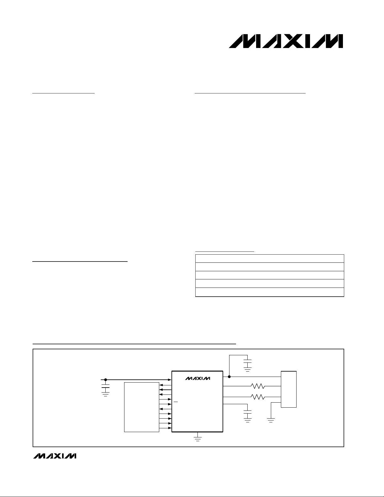
USB
INTERFACE
CONNECTOR
V
L
RCV
VPI
VMI
SUSP
D+
D-
V
BUS
D+
D-
GND
SYSTEM
SUPPLY
VOLTAGE
USB_DET
MODE
VTRM
ENUM
VPO
VMO
SYSTEM INTERFACE
V
CC
OE
23.7Ω
23.7Ω
MAX3344E/
MAX3345E
GND
0.1µF
1µF
1µF
Typical Operating Circuit
-40°C to +85°C
-40°C to +85°C
-40°C to +85°C
-40°C to +85°C
Page 2
MAX3344E/MAX3345E
±15kV ESD-Protected USB Transceivers
in UCSP with USB Detect
2 _______________________________________________________________________________________
ABSOLUTE MAXIMUM RATINGS
ELECTRICAL CHARACTERISTICS
(VCC= 4V to 5.5V bypassed with 1µF to GND, GND = 0, VL= 1.65V to 3.6V, ENUM = VL, TA= T
MIN
to T
MAX
, unless otherwise
noted. Typical values are at V
CC
= 5V, VL= 2.5V, TA= +25°C.) (Note 2)
Stresses beyond those listed under “Absolute Maximum Ratings” may cause permanent damage to the device. These are stress ratings only, and functional
operation of the device at these or any other conditions beyond those indicated in the operational sections of the specifications is not implied. Exposure to
absolute maximum rating conditions for extended periods may affect device reliability.
PARAMETER SYMBOL CONDITIONS
SUPPLY INPUTS (VCC, VTRM, VL)
Regulated Supply Voltage
Output
V
VTRM
Internal regulator 3.0 3.3 3.6 V
VCC Input Range V
CC
4.0 5.5 V
VL Input Range V
L
V
Operating VCC Supply Current I
VCC
Full-speed transmitting/receiving at
12Mbps, C
L
= 50pF on D+ and D-
10 mA
Operating VL Supply Current I
VL
Full-speed transmitting/receiving at
12Mbps
8mA
Full-speed idle: VD+ > 2.7V, VD- < 0.3V
Full-Speed Idle and SE0 Supply
Current
)
SE0: VD+ < 0.3V, VD- < 0.3V
µA
Static VL Supply Current
)
Full-speed idle, SE0, or suspend mode
µA
Suspend Supply Current
)
SUSP = OE = high 40 µA
Disable-Mode Supply Current I
VCC(DIS)
VL = GND or open 20 µA
D+/D- Disable-Mode
Load Current
I
D_(DIS)
VL = GND or open, VD_ = 0 or +5.5V 5 µA
Sharing-Mode VL Supply
Current
)
VCC = GND or open, OE = low, SUSP =
high
20 µA
D+/D- Sharing-Mode
Load Current
)
VCC = GND or open, VD_ = 0 or +5.5V 20 µA
LOGIC-SIDE I/O
Input High Voltage V
IH
SUSP, MODE, ENUM, OE, VMO, VPO 2/3 x V
L
V
Input Low Voltage V
IL
SUSP, MODE, ENUM, OE, VMO, VPO 0.4 V
Output-Voltage High V
OH
VPI, VMI, RCV, USB_DET; I
SOURCE
=
2mA
V
L
- 0.4 V
Output-Voltage Low V
OL
VPI, VMI, RCV, USB_DET; I
SINK
= -2mA 0.4 V
Note 1: External 23.7Ω resistors connected to D+ and D-.
(All voltages refer to GND, unless otherwise noted.)
Supply Voltage (V
CC
) ...............................................-0.3V to +6V
Output of Internal Regulator (VTRM)..........-0.3V to (V
CC
+ 0.3V)
Input Voltage (D+, D-)..............................................-0.3V to +6V
System Supply Voltage (V
L
) .....................................-0.3V to +6V
RCV, SUSP, VMO, MODE, VPO,
OE, VMI,
VPI, USB_DET, ENUM...............................-0.3V to (V
L
+ 0.3V)
Short-Circuit Current (D+, D-) to V
CC
or
GND (Note 1) .........................................................Continuous
Maximum Continuous Current (all other pins)..................±15mA
Continuous Power Dissipation (T
A
= +70°C)
16-Pin TSSOP (derate 9.4mW/°C above +70°C)...754mW (U16-2)
4
✕
4 UCSP (derate 8.2mW/°C above +70°C) ...659mW (B16-1)
Operating Temperature Range ...........................-40°C to +85°C
Junction Temperature......................................................+150°C
Storage Temperature Range .............................-65°C to +150°C
Lead Temperature (soldering, 10s) .................................+300°C
Bump Temperature (soldering) Reflow............................+235°C
MIN TYP MAX UNITS
1.65 3.60
I
VCC(IDLE
I
VL(STATIC
I
VCC(SUSP
340 450
390 500
I
VL(SHARING
I
D_(SHARING
12.5
Page 3
MAX3344E/MAX3345E
±15kV ESD-Protected USB Transceivers
in UCSP with USB Detect
_______________________________________________________________________________________ 3
ELECTRICAL CHARACTERISTICS (continued)
(VCC= 4V to 5.5V bypassed with 1µF to GND, GND = 0, VL= 1.65V to 3.6V, ENUM = VL, TA= T
MIN
to T
MAX
, unless otherwise
noted. Typical values are at V
CC
= 5V, VL= 2.5V, TA= +25°C.) (Note 2)
PARAMETER SYMBOL CONDITIONS
MIN
TYP
MAX
UNITS
Input Leakag e C ur r ent
S U SP , MOD E , E N UM , OE, VM O, V P O = 0 or
V
L
±1 µA
USB-SIDE I/O
Output-Voltage Low V
OL
RL = 1.5kΩ from D+ or D- to 3.6V 0.3 V
Output-Voltage High V
OH
RL = 15kΩ from D+ and D- to GND 2.8 3.6 V
Input Impedance Z
IN
Three-state driver, ENUM = 0, VD_ = 0 or
+3.6V
1MΩ
S i ng l e- E nd ed Inp ut- V ol tag e H i g h
V
IH
2.0 V
S i ng l e- E nd ed Inp ut- V ol tag e Low V
IL
0.8 V
Receiver Single-Ended
Hysteresis
V
HYS
mV
Differential Input Sensitivity V
DIFF
mV
Input Common-Mode Voltage
Range
V
CM
0.8 2.5 V
Driver Output Impedance R
OUT
4.6
Ω
Internal Pullup Resistor R
PU
kΩ
V
USBLH1
MAX3344E 4.0
V
USBHL1
MAX3344E 3.6
V
USBLH2
MAX3345E 2.8
USB_DET Threshold
V
USBHL2
MAX3345E 1
V
USB_DET Hysteresis V
USBHYS
MAX3344E 25 mV
LINEAR REGULATOR
External Capacitor C
OUT
Compensation of linear regulator 1 µF
ESD PROTECTION (VCC, D+, D-)
Human Body Model
kV
IE C 1000- 4- 2 Ai r - Gap D i schar g e
kV
IE C 1000- 4- 2 C ontact D i schar g e ±8 kV
TIMING CHARACTERISTICS
(VCC= 4V to 5.5V, GND = 0, VL= 1.65V to 3.6V, ENUM = VL, TA= T
MIN
to T
MAX
, unless otherwise noted. Typical values are at
V
CC
= 5V, VL= 2.5V, TA= +25°C.) (Figures 2–6) (Note 2)
PARAMETER
CONDITIONS
UNITS
TRANSMITTER
OE to Transmit Delay Enable Time t
PZD
Figures 2 and 6c 20 ns
OE to Driver Three-State Delay
Driver Disable Time
t
PDZ
Figures 2 and 6c 20 ns
)
MODE = high, Figures 4 and 6b 10 18
VPO/VMO to D+/D- Propagation
Delay
)
MODE = high, Figures 4 and 6b 10 18
ns
)
MODE = low, Figures 3 and 6c 11 20
VPO/VMO D+/D- Propagation
Delay
)
MODE = low, Figures 3 and 6c 11 20
ns
SYMBOL
t
PLH1(drv
t
PHL1(drv
t
PLH0(drv
t
PHL0(drv
200
1.410 1.500 1.540
MIN TYP MAX
200
±15
±10
16.0
Page 4
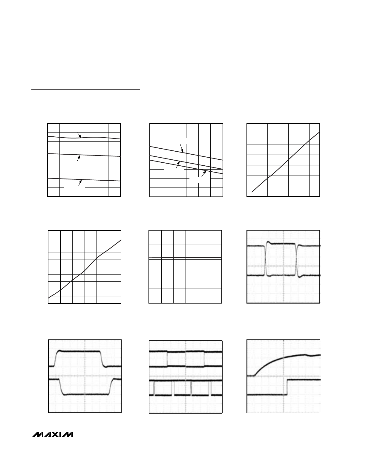
Typical Operating Characteristics
(VCC= 5V, VL= 3.3V, TA = +25°C, unless otherwise noted.)
MAX3344E/MAX3345E
±15kV ESD-Protected USB Transceivers
in UCSP with USB Detect
4 _______________________________________________________________________________________
TIMING CHARACTERISTICS (continued)
(VCC= 4V to 5.5V, GND = 0, VL= 1.65V to 3.6V, ENUM = VL, TA= T
MIN
to T
MAX
, unless otherwise noted. Typical values are at
V
CC
= 5V, VL= 2.5V, TA= +25°C.) (Figures 2–6) (Note 2)
PARAMETER
SYMBOL
CONDITIONS
MIN
TYP
MAX
UNITS
Rise Time D+/D- t
R1
CL = 50pF, 10% to 90% of
|V
OH
- VOL|
420ns
Fall Time D+/D- t
F1
CL = 50pF, 90% to 10% of
|V
OH
- VOL|
420ns
Rise- and Fall-Time Matching tR1/t
F1
(Note 3) 90 111 %
Output Signal Crossover V
CRS
(Note 3) 1.3 2.0 V
DIFFERENTIAL RECEIVER (Figures 5 and 6a)
)
18 ns
D+/D- to RCV Propagation Delay
)
18 ns
SINGLE-ENDED RECEIVERS (Figures 5 and 6a)
t
PLH(SE)
18 ns
D+/D- to VPI or VMI Propagation
Delay
t
PHL(SE)
18 ns
Note 2: Parameters are 100% production tested at 25°C, limits over temperature are guaranteed by design.
Note 3: Guaranteed by design, not production tested.
10
12
16
14
18
20
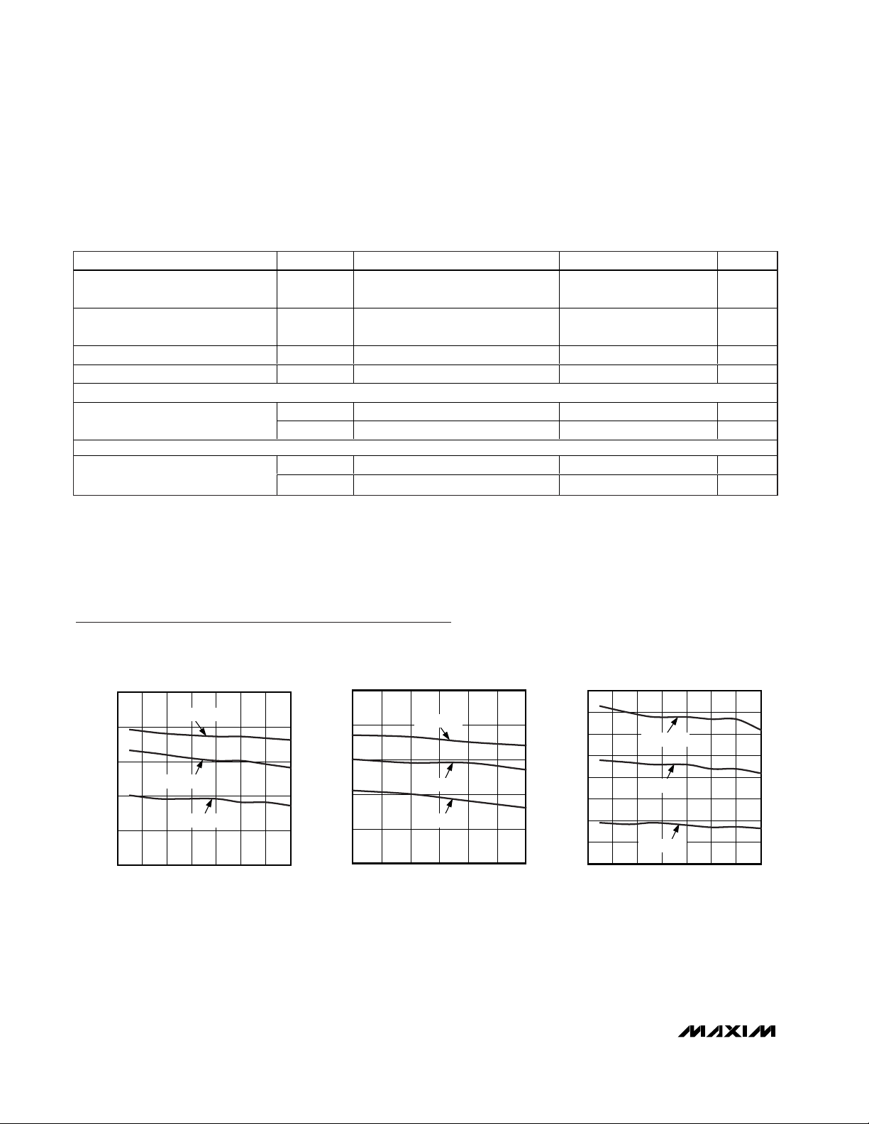
1.5 2.11.8 2.4 2.7 3.0 3.3 3.6
DIFFERENTIAL RECEIVER PROPAGATION
DELAY vs. V
L
MAX3344E/45E toc01
VL (V)
PROPAGATION DELAY (ns)
TA = -40°C
TA = +25°C
TA = +85°C
10
12
16
14
18
20
4.00 4.504.25 4.75 5.00 5.25 5.50
DIFFERENTIAL RECEIVER PROPAGATION
DELAY vs. V
CC
MAX3344E/45E toc02
VCC (V)
PROPAGATION DELAY (ns)
TA = -40°C
TA = +25°C
TA = +85°C
7
9
8
11
10
14
13
12
15
1.5 2.11.8 2.4 2.7 3.0 3.3 3.6
SINGLE-ENDED RECEIVER PROPAGATION
DELAY vs. V
L
MAX3344E/45E toc03
VL (V)
PROPAGATION DELAY (ns)
TA = -40°C
TA = +25°C
TA = +85°C
t
PLH(RCV
t
PHL(RCV
Page 5
MAX3344E/MAX3345E
±15kV ESD-Protected USB Transceivers
in UCSP with USB Detect
_______________________________________________________________________________________ 5
7
8
9
10
11
12
13
14
15
4.00 4.504.25 4.75 5.00 5.25 5.50
SINGLE-ENDED RECEIVER PROPAGATION
DELAY vs. V
CC
MAX3344E/45E toc04
VCC (V)
PROPAGATION DELAY (ns)
TA = -40°C
TA = +25°C
TA = +85°C
0.4
0.6
0.8
1.0
1.2
1.4
1.6
1.8
2.0
4.00 4.504.25 4.75 5.00 5.25 5.50
TRANSMITTER SKEW vs. V
CC
MAX3344E/45E toc05
VCC (V)
TRANSMITTER SKEW (ns)
TA = -40°C
TA = +25°C
TA = +85°C
3
5
4
7
6
9
8
10
1.5 2.1 2.41.8 2.7 3.0 3.3 3.6
LOGIC CURRENT CONSUMPTION IN
SUSPEND MODE
MAX3344E/45E toc06
VL (V)
I
VL
(µA)
22
25
24
23
26
27
28
29
30
31
32
4.00 4.504.25 4.75 5.00 5.25 5.50
V
CC
CURRENT CONSUMPTION IN
SUSPEND MODE
MAX3344E/45E toc07
VCC (V)
I
VCC
(µA)
3.0
3.1
3.3
3.2
3.4
3.5
4.00 4.504.25 4.75 5.00 5.25 5.50
VTRM vs. V
CC
MAX3344E/45E toc08
VCC (V)
VTRM (V)
I
VTRM
= 15mA
D-
D+
1V/div
RISE- AND FALL-TIME MATCHING
MAX3344E/45E toc09
20ns/div
f = 6MHz
2V/div
SUSP
SUSPEND RESPONSE
MAX3344E/45E toc10
100ns/div
0
0
RCV
2V/div
VPO
TRANSMISSION IN SUSPEND MODE
(SUSP = 1)
MAX3344E/45E toc11
2µs/div
VMO
D+
D-
USB_DET
V
CC
USB_DET RESPONSE
MAX3344E/45E toc12
10µs/div
0
0
2V/div
Typical Operating Characteristics (continued)
(VCC= 5V, VL= 3.3V, TA = +25°C, unless otherwise noted.)
Page 6

MAX3344E/MAX3345E
Detailed Description
The MAX3344E/MAX3345E are bidirectional transceivers
that convert single-ended or differential logic-level signals
to differential USB signals, and convert differential USB
signals to single-ended or differential logic-level signals.
The MAX3344E/MAX3345E are operational from VCC=
5.5V to VCC= 3V (electrical specifications are not guaranteed for VCC< 4V). Both devices include an internal
1.5kΩ pullup resistor that connects and disconnects D+
to VTRM (see the Functional Diagram).
The MAX3344E/MAX3345E are tolerant to power sequencing with either VCC> VLor VL> VCC. Additionally,
the USB I/O, D+ and D-, and VCCare ESD protected to
±15kV. The MAX3344E/MAX3345E can receive USB
power (VCC) directly from the USB connection and
operate with logic supplies (VL) down to 1.65V, while
still meeting the USB physical layer specifications. The
MAX3344E/MAX3345E support full-speed (12Mbps)
USB specification 2.0 operation.
The MAX3344E/MAX3345E have an enumerate feature
that functions when power is applied. Driving ENUM low
disconnects the internal 1.5kΩ pullup resistor from D+
enumerating the USB. This is useful if changes in communication protocol are required while power is applied, and
while the USB cable is connected.
±15kV ESD-Protected USB Transceivers
in UCSP with USB Detect
6 _______________________________________________________________________________________
Pin Description
PIN
TSSOP
NAME
IN PU T /
FUNCTION
1D2RCV
Receiver Output. Single-ended CMOS output. RCV responds to the differential input
on D+ and D-.
2D1VPO Input Logic-Level Data Input. VPO is level translated to D+.
3C2MODE Input
Mode-Control Input. Selects differential (mode 1) or single-ended (mode 0) input for
the system side when converting logic-level signals to USB level signals. Force
MODE high to select mode 1. Force MODE low to select mode 0.
4C1VMO Input Logic-Level Data Input. VMO is level translated to D-.
5B1OE Input
Output Enable. Drive OE low to enable data transmission on D+ and D-. Drive OE
high to disable data transmission or to receive data.
6B2SUSP Input
Suspend Input. Drive SUSP low for normal operation. Drive SUSP high for low-power
state. In low-power state, RCV is low and VPI/VMI are active.
7A1VPI
Logic-Level Data Output. VPI is the level-translated value of D+.
8A2VMI
Logic-Level Data Output. VMI is the level-translated value of D-.
9B3ENUM Input
Enumerate. Drive ENUM high to connect the internal 1.5kΩ resistor from D+ to 3.3V.
Drive ENUM low to disconnect the internal 1.5kΩ resistor.
10 A3 V
CC
Power
USB-Side Power-Supply Input. Connect V
CC
to the incoming USB power supply.
Bypass V
CC
to GND with a 1µF ceramic capacitor.
11 A4 GND Power Ground
12 B4 D-
Input/
Negative USB Differential Data Input/Output. Connect to the USB’s D- signal through
a 23.7Ω ±1% resistor.
13 C4 D+
Input/
Positive USB Differential Data Input/Output. Connect to the USB’s D+ signal through
a 23.7Ω ±1% resistor.
14 D4 VTRM Power
Reg ul ated Outp ut V ol tag e. V TRM p r ovi d es a 3.3V outp ut d er i ved fr om V
C C
. Byp ass
V TRM to G N D w i th a 1µF ( m i n) l ow - E S R cap aci tor , such as cer am i c or p l asti c fi l m typ es.
15 D3 V
L
Power
S ystem - S i d e P ow er - S up p l y Inp ut. C onnect to the system ’ s l og i c- l evel p ow er sup p l y,
1.65V to 3.6V .
16 C3
USB Detector Output. A high at USB_DET signals to the ASIC that VCC is present. A
low at USB_DET indicates that V
CC
is not present. The MAX3344E USB_DET
threshold is between 3.6V (min) and 4V (max), while the MAX3345E USB_DET
threshold is between 1V (min) and 2.8V (max).
UCSP
O U T PU T
Output
Output
Output
Output
Output
USB_DET Output
Page 7

Power-Supply Configurations
Normal Operating Mode
Connect VLand VCCto system power supplies (Table
1). Connect VLto a +1.65V to +3.6V supply. Connect
VCCto a +4.0V to +5.5V supply. Alternatively, the
MAX3344E/MAX3345E can derive power from a single
Li+ battery. Connect the battery to V
CC.VVTRM
remains
above +3.0V for V
CC
as low as +3.1V.
Additionally, the MAX3344E/MAX3345E can derive
power from a 3.3V ±10% voltage regulator. Connect V
CC
and VTRM to an external +3.3V voltage regulator.
Disable Mode
Connect VCCto a system power supply and leave V
L
unconnected or connect to GND. D+ and D- enter a tristate mode and VCCconsumes less than 20µA of supply
current. D+ and D- withstand external signals up to
+5.5V in disable mode (Table 2).
Sharing Mode
Connect V
L
to a system power supply and leave VCC(or
VCCand VTRM) unconnected or connect to GND. D+
and D- enter a tri-state mode, allowing other circuitry to
share the USB D+ and D- lines, and V
L
consumes less
than 20µA of supply current. D+ and D- withstand external signals up to +5.5V in sharing mode (Table 2).
Device Control
D+ and D-
D+ and D- are the USB-side transmitter I/O connections, and are ESD protected to ±15kV using the
Human Body Model, ±10kV using IEC 1000-4-2 AirGap Discharge, and ±8kV using IEC 1000-4-2 Contact
Discharge, making the MAX3344E/MAX3345E ideal for
applications where a robust transmitter is required. A
23.7Ω resistor is required on D+ and D- for normal
operation (see the External Resistors section).
ENUM
USB specification 2.0 requires a 1.5kΩ pullup resistor
on D+ for full-speed (12Mbps) operation. Controlled by
enumerate (ENUM), the MAX3344E/MAX3345E provide
this internal 1.5kΩ resistor. Drive ENUM high to connect
the pullup resistor from D+ to VTRM. Drive ENUM low to
disconnect the pullup resistor from D+ to VTRM.
VPO/VMO, VPI/VMI, and
OE
The MAX3344E/MAX3345E system-side inputs are VPO
and VMO. Data comes into the MAX3344E/MAX3345E
through VPO and VMO. VPO and VMO operate either
differentially with VPO as the positive terminal and VMO
as the negative terminal, or single ended with VPO as
the data input (see the MODE section).
MAX3344E/MAX3345E
±15kV ESD-Protected USB Transceivers
in UCSP with USB Detect
_______________________________________________________________________________________ 7
VCC (V) VTRM (V) VL (V) CONFIGURATION NOTES
+4.0 to +5.5 +3.3 Output +1.65 to +3.6 Normal mode —
+3.1 to +4.5 +3.3 Output +1.65 to +3.6 Battery supply —
+3.0 to +3.6 +3.0 to +3.6 Input +1.65 to +3.6 Voltage regulator supply —
GND or floating Output +1.65 to +3.6 Sharing mode Table 2
+3.0 to +5.5 Output GND or floating Disable mode Table 2
INPUTS/OUTPUTS DISABLE MODE SHARING MODE
VCC/VTRM
• +5V input/+3.3V output
• +3.3V input/+3.3V input
• +3.7V input/+3.3V output
• Floating or connected to GND
• < +3.6V (MAX3344E)
• < +1.0V (MAX3345E)
V
L
Floating or connected to GND +1.65V to +3.6V input
D+ and D- High impedance High impedance
High impedance for OE = Low
VPI and VMI Invalid*
High for OE = High
RCV Invalid* Undefined**
SPEED, SUSP, OE, ENUM High impedance High impedance
Table 2. Disable-Mode and Sharing-Mode Configurations
Table 1. Power-Supply Configurations
*High Impedance or low.
**High or low.
Page 8

MAX3344E/MAX3345E
±15kV ESD-Protected USB Transceivers
in UCSP with USB Detect
8 _______________________________________________________________________________________
The MAX3344E/MAX3345E system-side outputs are
VPI, VMI, and RCV. The MAX3344E/MAX3345E send
data through VPI, VMI, and RCV. VPI and VMI are outputs to the single-ended receivers and RCV is the output of the differential receiver.
Output enable (OE) controls data transmission. Drive OE
low to enable data transmission on D+ and D-. Drive OE
high to disable data transmission or receive data.
MODE
MODE is a control input that selects whether differential
or single-ended logic signals are recognized by the
system side of the MAX3344E/MAX3345E. Drive MODE
high to select differential mode with VPO as the positive
terminal and VMO as the negative terminal. Drive
MODE low to select single-ended mode with VPO as
the data input (Table 3).
VTRM
VTRM is the 3.3V output of the internal linear voltage
regulator. VTRM powers the internal circuitry of the USB
side of the MAX3344E/MAX3345E. Connect a 1µF (min)
low-ESR ceramic or plastic capacitor from VTRM to
GND, as close to VTRM as possible. Do not use VTRM
to power external circuitry.
V
CC
Bypass VCCto GND with a 1µF ceramic capacitor as
close to the device as possible. If VCCdrops below the
USB detect threshold, supply current drops
below 20µA avoiding excessive VCCcurrent consumption, and D+/D- enter a high-impedance state allowing
other devices to drive the lines.
USB Detect
USB detect output (USB_DET) signals that VCCis present. A high at USB_DET indicates that VCCis present,
while a low at USB_DET indicates that V
CC
is not pre-
sent. The MAX3344E USB_DET threshold is between
3.6V (min) and 4V (max), while the MAX3345E USB_DET
threshold is between 1V (min) and 2.8V (max).
SUSP
Suspend (SUSP) is a control input. Force SUSP high to
place the MAX3344E/MAX3345E in a low-power state.
In this state, the quiescent supply current into VCCis
less than 40µA and RCV goes low.
In suspend mode, VPI and VMI remain active as
receive outputs and VTRM stays on. The MAX3344E/
MAX3345E continue to receive data from the USB,
allowing the µP to sense activity on the D+/D- lines and
wake up the MAX3344E/MAX3345E.
The MAX3344E/MAX3345E can also transmit data to
D+ and D- while in suspend mode. This function is
used to signal a remote wake-up by driving a signal on
D+ and D- for a period of 1ms to 15ms. In suspend
mode, data can only be transmitted with full-speed
slope control.
Figure 1c. IEC 1000-4-2 ESD Test Model
CHARGE-CURRENT-
LIMIT RESISTOR
DISCHARGE
RESISTANCE
STORAGE
CAPACITOR
C
s
150pF
R
C
50MΩ TO 100MΩ
R
D
330Ω
HIGH-
VOLTAGE
DC
SOURCE
DEVICE
UNDER
TEST
Figure 1b. Human Body Model Current Waveform
IP 100%
90%
36.8%
t
RL
TIME
t
DL
CURRENT WAVEFORM
PEAK-TO-PEAK RINGING
(NOT DRAWN TO SCALE)
I
r
10%
0
0
AMPERES
Figure 1a. Human Body ESD Test Models
CHARGE-CURRENT-
LIMIT RESISTOR
DISCHARGE
RESISTANCE
STORAGE
CAPACITOR
C
s
100pF
R
C
1MΩ
R
D
1500Ω
HIGH-
VOLTAGE
DC
SOURCE
DEVICE
UNDER
TEST
Page 9

MAX3344E/MAX3345E
±15kV ESD-Protected USB Transceivers
in UCSP with USB Detect
_______________________________________________________________________________________ 9
Data Transfer
Receiving Data from the USB
Data received from the USB are output to VPI/VMI in
either of two ways, differentially or single ended. To
receive data from the USB, force OE high and SUSP low.
Differential data arriving at D+/D- appear as differential
logic signals at VPI/VMI, and as a single-ended logic signal at RCV. If both D+ and D- are low, then VPI and VMI
are low, signaling a single-ended zero condition on the
bus; RCV remains in the last known state (Table 3).
Transmitting Data to the USB
The MAX3344E/MAX3345E output data to the USB differentially on D+ and D-. The logic driving signals can
be either differential or single ended. For sending differential logic, force MODE high, force OE and SUSP low,
and apply data to VPO and VMO. D+ then follows VPO,
and D- follows VMO. To send single-ended logic signals, force MODE, SUSP, and OE low, and apply data to
VPO/VMO.
ESD Protection
To protect the MAX3344E/MAX3345E against ESD, D+
and D- have extra protection against static electricity to
protect the device up to ±15kV. The ESD structures
withstand high ESD in all states—normal operation,
suspend, and powered down. For the 15kV ESD structures to work correctly, a 1µF or greater capacitor must
be connected from VTRM to GND.
ESD protection can be tested in various ways; the D+
and D- input/output pins are characterized for protection
to the following limits:
1) ±15kV using the Human Body Model
2) ±8kV using the IEC 1000-4-2 Contact Discharge
Method
3) ±10kV using the IEC 1000-4-2 Air-Gap Method
ESD Test Conditions
ESD performance depends on a variety of conditions.
Contact Maxim for a reliability report that documents test
setup, test methodology, and test results.
Human Body Model
Figure 1a shows the Human Body Model, and Figure 1b
shows the current waveform it generates when discharged into a low impedance. This model consists of a
100pF capacitor charged to the ESD voltage of interest,
which is then discharged into the test device through a
1.5kΩ resistor.
D+/D-
t
PDZ
t
PZD
V
OHD
- 0.3V
V
OLD
+ 0.3V
V
L
0V
VL/2
OE
Figure 2. Enable and Disable Timing, Transmitter
VPO
t
PHLO
V
L
0V
D+
D-
0V
VTRM
VL/2
t
PLHO
Figure 3. Mode 0 Timing
t
PLH1
V
L
0V
0V
VTRM
VL/2
D+
D-
VMO
V
L
0V
t
PHL1
VL/2
t
PLH1
t
PLH1
VL/2
VPO
Figure 4. Mode 1 Timing
Page 10

MAX3344E/MAX3345E
±15kV ESD-Protected USB Transceivers
in UCSP with USB Detect
10 ______________________________________________________________________________________
Table 3a. Truth Table Transmit (SUSP = 0, OE = 0, ENUM = X)
INPUT OUTPUT
MODE VPO VMO D+ D- RCV VPI VMI RESULT
00001001LOGIC 0
00100RCV* 0 0 SE0
01010110LOGIC 1
01100RCV* 0 0 SE0
10000RCV* 0 0 SE0
10101001LOGIC 0
11010110LOGIC 1
11111X11
UNDEFINED
Table 3b. Truth Table Receive (SUSP = 0, OE = 1, ENUM = X)
INPUT OUTPUT
D+ D- RCV
VPI
VMI
RESULT
00RCV* 0 0 SE0
01001LOGIC 0
10110LOGIC 1
11X11UNDEFINED
*Timing specifications are not guaranteed for D+ and D-.
Table 3c. Truth Table Transmit in Suspend* (SUSP = 1, OE = 0, ENUM = X)
INPUT OUTPUT
MODE VPO VMO D+ D- RCV VPI VMI RESULT
00001001LOGIC 0
00100000SE0
01010010LOGIC 1
01100000SE0
10000000SE0
10101001LOGIC 0
11010010LOGIC 1
11111011
UNDEFINED
Table 3d. Truth Table Receive in Suspend* (SUSP = 1, OE = 1, MODE = X, VPO/VMO = X,
ENUM = X)
*Timing specifications are not guaranteed for D+ and D-.
*RCV denotes the signal level on output RCV just before SE0 state occurs. This level is stable during the SE0 period.
*RCV denotes the signal level on output RCV just before SE0 state occurs. This level is stable during the SE0 period.
D+ D- RCV
00000VPI/VMI ACTIVE
01001VPI/VMI ACTIVE
10010VPI/VMI ACTIVE
11011VPI/VMI ACTIVE
INPUT OUTPUT
VPI VMI
RESULT
Page 11

IEC 1000-4-2
The IEC 1000-4-2 standard covers ESD testing and performance of finished equipment; it does not specifically
refer to integrated circuits. The MAX3344E/MAX3345E
help the user design equipment that meets level 4 of IEC
1000-4-2, without the need for additional ESD-protection
components.
The major difference between tests done using the
Human Body Model and IEC 1000-4-2 is a higher peak
current in IEC 1000-4-2, because series resistance is
lower in the IEC 1000-4-2 model. Hence, the ESD withstand voltage measured to IEC 1000-4-2 is generally
lower than that measured using the Human Body Model.
Figure 1c shows the IEC 1000-4-2 model.
The Air-Gap Discharge Method involves approaching
the device with a charged probe. The Contact
Discharge Method connects the probe to the device
before the probe is energized.
Machine Model
The Machine Model for ESD tests all pins using a 200pF
storage capacitor and zero discharge resistance. Its
objective is to emulate the stress caused by contact that
occurs with handling and assembly during manufacturing. All pins require this protection during manufacturing. Therefore, after PC board assembly, the Machine
Model is less relevant to I/O ports.
Applications Information
External Components
External Resistors
Two external 23.7Ω ±1% to 27.4Ω ±1%, 1/2W resistors
are required for USB connection. Place the resistors
in between the MAX3344E/MAX3345E and the USB
connector on the D+ and D- lines (see the Typical
Operating Circuit).
External Capacitors
Use three external capacitors for proper operation. Use
a 0.1µF ceramic for decoupling VL, a 1µF ceramic for
decoupling VCC, and a 1.0µF (min) ceramic or plastic
filter capacitor on VTRM. Return all capacitors to GND.
UCSP Applications Information
For the latest application details on UCSP construction,
dimensions, tape carrier information, printed circuit board
techniques, bump-pad layout, and recommended reflow
temperature profile, as well as the latest information on
reliability testing results, refer to the Application Note
UCSP—A Wafer-Level Chip-Scale Package available on
Maxim’s website at www.maxim-ic.com/ucsp.
MAX3344E/MAX3345E
±15kV ESD-Protected USB Transceivers
in UCSP with USB Detect
______________________________________________________________________________________ 11
Chip Information
TRANSISTOR COUNT: 2162
PROCESS: BiCMOS
Page 12

MAX3344E/MAX3345E
±15kV ESD-Protected USB Transceivers
in UCSP with USB Detect
12 ______________________________________________________________________________________
t
PHL(RCV)
t
PLH(RCV)
t
PHL(SE)
t
PLH(SE)
t
PLH(SE)
t
PHL(SE)
D+
D-
RCV
VPI
VMI
D+/D- RISE/FALL TIMES ≤ 8ns, V
L
= 1.65V, 2.5V, 3.3V
3V
0V
V
L
VL/2
V
L
/2
V
L
/2
0V
V
L
0V
V
L
0V
Figure 5. D+/D- to RCV, VPI, VMI Propagation Delays
(c) LOAD FOR ENABLE AND DISABLE TIME, D+/D-
(a) LOAD FOR VPI, VMI, AND RCV
VMI OR VPI OR RCV
MAX3344E
MAX3345E
25pF
TEST POINT
D+ OR D-
200Ω23.7Ω
MAX3344E
MAX3345E
50pF
GND
OR V
CC
+
-
TEST POINT
D+
D-
USB_DET
23.7Ω
C
L
= 50pF
C
L
= 50pF
15kΩ
1.5kΩ
3.3V
MAX3344E
MAX3345E
TEST POINT
(b) LOAD FOR D+, D-, AND USB_DET
23.7Ω
15kΩ
TEST POINT
25pF
Figure 6. Test Circuits
Page 13

MAX3344E/MAX3345E
±15kV ESD-Protected USB Transceivers
in UCSP with USB Detect
______________________________________________________________________________________ 13
LINEAR
REGULATOR
TO INTERNAL CIRCUITS
23.7Ω
ENUM
GND
VMI
VPI
RCV
SUSP
MODE
V
L
VPO
OE
V
CC
VTRM
D-
D+
MAX3344E
MAX3345E
BANDGAP
TO INTERNAL CIRCUITS
EXTERNAL RESISTORS
23.7Ω
VMO
1.5kΩ
SINGLE-ENDED RECEIVERS
Vbg
Vbg
USB SUPPLY
TRANSMITTER
RECEIVER
USB_DET
Functional Diagram
16
15
14
13
12
11
10
1
2
3
4
5
6
7
USB_DET
V
L
VTRM
D+
D-
VMO
MODE
VPO
RCV
TOP VIEW BOTTOM VIEW
MAX3344E
MAX3345E
GND
V
CC
9ENUM
VPI
8VMI
SUSP
TSSOP
UCSP
V
CC
V
L
GND
VTRM
D+
D-
VMI
MODE
RCV
SUSP
USB_DET
ENUM
VMO
VPO
VPI
MAX3344E/MAX3345E
A
B
C
D
1234
OE
OE
Pin Configurations
Page 14

MAX3344E/MAX3345E
±15kV ESD-Protected USB Transceivers
in UCSP with USB Detect
14 ______________________________________________________________________________________
Package Information
(The package drawing(s) in this data sheet may not reflect the most current specifications. For the latest package outline information,
go to www.maxim-ic.com/packages
.)
16L,UCSP.EPS
PACKAGE OUTLINE, 4x4 UCSP
21-0101
1
H
1
Page 15

MAX3344E/MAX3345E
±15kV ESD-Protected USB Transceivers
in UCSP with USB Detect
Maxim cannot assume responsibility for use of any circuitry other than circuitry entirely embodied in a Maxim product. No circuit patent licenses are
implied. Maxim reserves the right to change the circuitry and specifications without notice at any time.
Maxim Integrated Products, 120 San Gabriel Drive, Sunnyvale, CA 94086 408-737-7600 ____________________ 15
© 2004 Maxim Integrated Products Printed USA is a registered trademark of Maxim Integrated Products.
TSSOP4.40mm.EPS
Package Information (continued)
(The package drawing(s) in this data sheet may not reflect the most current specifications. For the latest package outline information,
go to www.maxim-ic.com/packages
.)
 Loading...