

Page 1
19-5214; Rev 0; 4/10
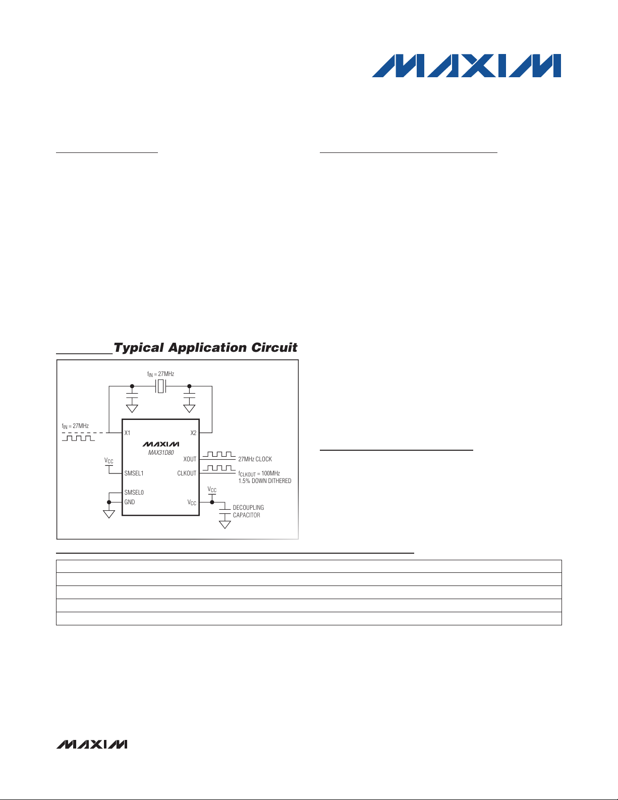
Typical Application Circuit
MAX31D80
X1
SMSEL1
SMSEL0
GND
X2
XOUT 27MHz CLOCK
DECOUPLING
CAPACITOR
f
IN
= 27MHz
V
CC
fIN = 27MHz
CLKOUT
V
CC
f
CLKOUT
= 100MHz
1.5% DOWN DITHERED
V
CC
Spread-Spectrum Clock Generators
General Description
The MAX31C80/MAX31D80 are spread-spectrum clock
generators that contain a phase-locked loop (PLL)
that generates a 2MHz to 134MHz clock from an input
clock or crystal. The PLL can provide a spread-spectrum down-dithered (MAX31D80) or center-dithered
(MAX31C80) frequency-modulated clock. The devices
also buffer the incoming clock and provide this output
on a separate pin.
The MAX31C80/MAX31D80 are provided in a 10-pin
TDFN package and operate over a full -40NC to +125NC
automotive temperature range. Devices can be factory
programmed for multiple combinations of input and output frequencies (see the Ordering Information table). A
low-cost, low-frequency crystal can be used at the input
to generate frequencies up to 134MHz.
MAX31C80/MAX31D80
Features
S 2MHz to 134MHz Spread-Spectrum Clock
Generator
S Input Can Be Either an 8MHz to 34MHz Crystal or
8MHz to 134MHz Clock
S Factory-Programmable Output Frequencies in
2MHz to 134MHz Range
S Low-Cost Crystal at Low Frequency Used to
Generate High Frequencies
S On-Board PLL is Capable of Spread-Spectrum
Frequency Modulation
S Down- or Center-Dither Spread-Spectrum
Frequency Modulation
S User-Configurable Spread-Spectrum Dither
Magnitude
S Low Cycle-to-Cycle Jitter
S 3.3V Supply Voltage
S Temperature Range: -40NC to +125NC
S Small Package: 10-Pin TDFN (3mm x 3mm x
0.8mm)
Ordering Information
PART TEMP RANGE DITHER MODE PIN-PACKAGE
MAX31C80T-xxx+
MAX31C80T-xxx+T
MAX31D80T-xxx+
MAX31D80T-xxx+T
_______________________________________________________________ Maxim Integrated Products 1
xxx = Factory-programmable output frequency and dither rate (see the Selector Guide table).
+Denotes a lead(Pb)-free/RoHS-compliant package.
T = Tape and reel.
*EP = Exposed pad.
Selector Guide appears at end of data sheet.
For pricing, delivery, and ordering information, please contact Maxim Direct at 1-888-629-4642,
or visit Maxim’s website at www.maxim-ic.com.
-40NC to +125NC
-40NC to +125NC
-40NC to +125NC
-40NC to +125NC
Applications
Graphics Cards
Set-Top Boxes
Automotive Infotainment
Printers
Center 10 TDFN-EP*
Center 10 TDFN-EP*
Down 10 TDFN-EP*
Down 10 TDFN-EP*
Page 2
Spread-Spectrum Clock Generators
ABSOLUTE MAXIMUM RATINGS
Voltage Range on VCC Relative to GND ..............-0.3V to +4.3V
Voltage Range on Any Other Pin
Relative to GND .................................... -0.3V to (VCC + 0.3V)*
Continuous Power Dissipation (TA = +70°C)
10-Pin TDFN (derate 24.4mW/°C above +70°C) .....1951.2mW
*Not to exceed +4.3V.
Stresses beyond those listed under “Absolute Maximum Ratings” may cause permanent damage to the device. These are stress ratings only, and
functional operation of the device at these or any other conditions beyond those indicated in the operational sections of the specifications is not implied.
Exposure to absolute maximum rating conditions for extended periods may affect device reliability.
RECOMMENDED OPERATING CONDITIONS
(TA = -40NC to +125NC.)
PARAMETER SYMBOL CONDITIONS MIN TYP MAX UNITS
Supply Voltage V
Input Logic 0
(SMSEL0 and SMSEL1)
Input Logic 1
MAX31C80/MAX31D80
(SMSEL0 and SMSEL1)
Input Logic Unconnected
(SMSEL0 and SMSEL1)
Input Logic 0 for X1 V
Input Logic 1 for X1 V
XOUT Load C
CLKOUT Load C
Crystal Frequency f
Clock Input Frequency f
Crystal ESR X
Clock Input Duty Cycle f
Crystal Parallel Load
Capacitance
CC
V
IL
V
IH
V
IF
IL:X1
IH:X1
L:XOUT
L:CLKOUT
IN
IN
ESR
INDC
C
CL
Limits are in case user wants to force
voltage instead of unconnecting this pin
2MHz P f
67MHz P f
101MHz P f
CLKOUT
CLKOUT
Storage Temperature Range ............................ -55NC to +135NC
Lead Temperature (soldering, 10s) ................................+300NC
Soldering Temperature (reflow) ......................................+260NC
3.0 3.3 3.6 V
0.25 x
VCC +
0.55 x
VCC +
< 67MHz
CLKOUT
< 101MHz
P 134MHz
-0.3
0.75 x
V
CC
0.4 x
V
CC
-0.3
0.7 x
V
CC
8 34 MHz
8 134 MHz
40 60 %
V
CC
0.3
V
CC
0.3 x
V
CC
0.3
15 pF
15
10
7
90
18 pF
pF
V
V
V
V
V
I
2 ______________________________________________________________________________________
Page 3
Spread-Spectrum Clock Generators
DC ELECTRICAL CHARACTERISTICS
(3.0V P VCC P 3.6V, TA = -40NC to +125NC, unless otherwise noted.)
PARAMETER SYMBOL CONDITIONS MIN TYP MAX UNITS
Supply Current I
Input Leakage
(SMSEL0 and SMSEL1)
Low-Level Output Voltage
(XOUT and CLKOUT)
High-Level Output Voltage
(XOUT and CLKOUT)
Input Capacitance
(X1 and X2)
DD
I
IL
V
OL
V
OH
C
IN
fIN = 27MHz, f
dithered, CL = 10pF
SMSEL_ = GND or V
IOL = 10mA 0.2 V
IOH = -10mA
CLKOUT
AC ELECTRICAL CHARACTERISTICS
(3.0V P VCC P 3.6V, TA = -40NC to +125NC, unless otherwise noted.)
PARAMETER SYMBOL CONDITIONS MIN TYP MAX UNITS
CLKOUT Duty Cycle f
XOUT Duty Cycle f
Rise Time t
Fall Time t
Dither Rate Range f
Dither Rate Accuracy -4 +4 %
Peak Cycle-to-Cycle Jitter t
Power-Up Time t
CLKOUT:DCCL:CLKOUT
C
XOUT:DC
R
F
DR
J
PUP
L:XOUT
VCC = 3.3V
C
L:CLKOUT
C
L:CLKOUT
Factory programmable 20 40 kHz
CLKOUT = 100MHz, 10,000 cycles,
TA = +25NC
VCC valid to output active, TA = +25NC,
VCC = 3.3V
= 7pF 40 60
= 7pF, TA = +25NC,
= 7pF 1.6 ns
= 7pF 1.6 ns
= 100MHz, down
CC
22 mA
Q15 FA
VCC -
0.2
5 pF
40 60
75 ps
1 ms
MAX31C80/MAX31D80
V
%
_______________________________________________________________________________________ 3
Page 4

Spread-Spectrum Clock Generators
Typical Operating Characteristics
(V
= +3.3V, T
CC
= +25°C, unless otherwise noted.)
A
SUPPLY CURRENT
vs. SUPPLY VOLTAGE
27
fIN = 27MHz
= 100MHz
f
CLKOUT
25
23
21
19
SUPPLY CURRENT (mA)
17
15
TA = -40°C
3.0 3.6
SUPPLY VOLTAGE (V)
MAX31C80/MAX31D80
DUTY CYCLE (%)
TA = +125°C
TA = +25°C
3.43.2
vs. SUPPLY VOLTAGE
60
f
= 100MHz
CLKOUT
58
56
54
52
TA = +25°C
50
48
46
44
42
40
3.0 3.6
SUPPLY VOLTAGE (V)
MAX31C80 toc01
DUTY CYCLE
TA = +125°C
TA = -40°C
3.43.2
fIN = 27MHz
29
f
CLKOUT
27
25
23
21
SUPPLY CURRENT (mA)
19
17
15
-40
MAX31C80 toc04
SUPPLY CURRENT
vs. TEMPERATURE
= 100MHz
VCC = 3.0V
TEMPERATURE (°C)
VCC = 3.6V
VCC = 3.3V
60
58
56
54
52
50
48
DUTY CYCLE (%)
46
44
42
40
-40
11085-15 10 35 60
f
CLKOUT
MAX31C80 toc02
= 100MHz
25
VCC = 3.3V
20
15
10
SUPPLY CURRENT (mA)
5
0
8
DUTY CYCLE
vs. TEMPERATURE
VCC = 3.6V
VCC = 3.0V
TEMPERATURE (°C)
VCC = 3.3V
SUPPLY CURRENT
vs. OUTPUT FREQUENCY
MAX31C80 toc03
104805632
OUTPUT FREQUENCY (MHz)
MAX31C80 toc05
1106010
FREQUENCY SPECTRUM AT 122MHz
WITH CENTER SPREAD
0
f
= 122MHz
CLKOUT
CENTER DITHER = ±1.5%
-10
-20
-30
ATTENUATION (dB)
-40
-50
-60
119.2
FREQUENCY (MHz)
-14.23dB
123.2121.2
MAX31C80 toc06
FREQUENCY SPECTRUM AT 100MHz
WITH DOWN DITHER
0
f
= 100MHz
CLKOUT
CENTER DITHER = -3%
-10
-20
-30
ATTENUATION (dB)
-40
-50
-60
96
FREQUENCY (MHz)
-16.56dB
10098
4 ______________________________________________________________________________________
MAX31C80 toc07
Page 5

Block Diagram
Pin Description
8MHz TO 134MHz CLOCK
OR
8MHz TO 34MHz CRYSTAL
f
IN
Spread-Spectrum Clock Generators
V
MAX31C80
MAX31D80
X1
CRYSTAL
X2
OSCILLATOR
PROGRAMMABLE
PLL WITH SPREAD
SPECTRUM
CC
V
CC
CLKOUT
(f
= 2MHz TO 134MHz)
CLKOUT
XOUT
(f
= fIN)
XOUT
MAX31C80/MAX31D80
SMSEL0
SMSEL1
SPREAD-SPECTRUM
MAGNITUDE CONTROL
GND
Pin Configuration
TOP VIEW
X2
10 8 7
+
1 3 4
X1
SMSEL1
9
MAX31C80
MAX31D80
2
SMSEL0
TDFN
VCCGND
CC
V
GND
XOUTCLKOUT
6
EP
5
PIN NAME FUNCTION
Crystal Drive/Clock Input. A crystal with
the proper loading is connected across
1 X1
X1 and X2. Instead of a crystal, a clock
can be applied at the X1 input. If no
clock or crystal is present, then no clock
is output at either XOUT or CLKOUT.
Spread-Spectrum Magnitude Select.
These are three-state digital inputs
2, 9
SMSEL0,
SMSEL1
to determine the spread-spectrum
magnitude. Tables 1 and 2 provide
details for configuration of these pins for
down and center dither, respectively.
PIN NAME FUNCTION
3, 8 V
CC
Supply Voltage
4, 7 GND Ground
5 CLKOUT
6 XOUT
Clock Output. Spread-spectrum-capable
digital output clock from the PLL.
Crystal Buffered Output. Buffered digital
output of the input crystal or clock.
Crystal Drive Output. A crystal with the
10 X2
proper loading is connected across X1
and X2. If a clock is applied at the X1
input, then X2 should be left open circuit.
— EP Exposed Pad. Connect to GND.
_______________________________________________________________________________________ 5
Page 6

Spread-Spectrum Clock Generators
Detailed Description
The MAX31C80/MAX31D80 modulate an input clock to
generate a center-dithered or down-dithered spreadspectrum output. An 8MHz to 27MHz crystal or 8MHz
to 134MHz oscillator input is applied to the device. An
internal PLL dithers the output clock at a user-selectable magnitude to produce a down-dithered or centerdithered output clock. The output clock’s frequency is
programmable from 2MHz to 134MHz. The devices also
buffer the incoming clock and provide this output on a
separate pin.
Spread-Spectrum Dither Magnitude
The MAX31D80 can generate down-dithered magnitudes
up to -3%. The MAX31C80 can generate center-dithered
magnitudes up to P 1.5%. The desired magnitude is
selected using the input pins SMSEL1 and SMSEL0 as
shown in Tables 1 and 2. A power cycle is required after
each change of the dither magnitude for the changes to
take effect.
Table 1. Spread-Spectrum Mode and Magnitude Select (for Down Dither)
SMSEL1 SMSEL0
0 0 Spread-Spectrum Disabled
0 Unconnected 0 to -0.25
0 1 0 to -0.375
MAX31C80/MAX31D80
Unconnected 0 0 to -0.5
Unconnected Unconnected 0 to -0.75
Unconnected 1 0 to -1.0
1 0 0 to -1.5
1 Unconnected 0 to -2.0
1 1 0 to -3.0
SPREAD-SPECTRUM MAGNITUDE
SELECTED (%)
SPREAD-SPECTRUM DITHER MODE
SELECTED
Down Dither
Table 2. Spread-Spectrum Mode and Magnitude Select (for Center Dither)
SMSEL1 SMSEL0
0 0 Spread-Spectrum Disabled
0 Unconnected -0.25 to +0.25
0 1 -0.375 to +0.375
Unconnected 0 -0.5 to +0.5
Unconnected Unconnected -0.75 to +0.75
Unconnected 1 -1.0 to +1.0
1 0 -1.5 to +1.5
1 Unconnected N/A
1 1 N/A
6 ______________________________________________________________________________________
SPREAD-SPECTRUM MAGNITUDE
SELECTED (%)
SPREAD-SPECTRUM DITHER MODE
SELECTED
Center Dither
Page 7

Spread-Spectrum Clock Generators
DOWN DITHERED (MAX31D80)
MAX31C80/MAX31D80
FREQUENCY
f
CLKOUT
f
- (0.25% TO 3%)
CLKOUT
1
DITHER CYCLE
RATE
Figure 1. Spread-Spectrum Frequency Modulation (Down Dithered)
CENTER DITHERED (MAX31C80)
FREQUENCY
f
+ (0.25% TO 1.5%)
CLKOUT
f
IN
f
- (0.25% TO 1.5%)
CLKOUT
IF SMSEL0 = SMSEL1 = 0
DITHER AMOUNT
(-0.25% TO -3.0%)
TIME
IF SMSEL0 = SMSEL1 = 0
DITHER AMOUNT
(±0.25% TO ±1.5%)
1
DITHER CYCLE
RATE
Figure 2. Spread-Spectrum Frequency Modulation (Center Dithered)
_______________________________________________________________________________________ 7
TIME
Page 8

Spread-Spectrum Clock Generators
Factory Programmability
The MAX31C80/MAX31D80 can provide a variety of fre-
V
CC
XOUT
CLKOUT
Figure 3. Power-Up Timing
MAX31C80/MAX31D80
VCC VALID
t
PUP
OUTPUT VALID
OUTPUT VALID
Selector Guide
quencies, which are available to users by ordering the
device according to specifications listed in the Selector
Guide table.
Email the factory at custom.oscillators@maxim-ic.com
to obtain custom output frequencies for specific input
frequencies not mentioned in the Selector Guide table.
Applications Information
Power-Supply Decoupling
To achieve best results, it is highly recommended that a
decoupling capacitor be used on the IC power-supply
pins. Typical values of decoupling capacitors are 0.01FF
and 0.1FF. Use a high-quality, ceramic, surface-mount
capacitor and mount it as close as possible to the VCC
pins of the IC to minimize lead inductance.
PART
MAX31C80T-UGQ+ 27 100 31.25 Center
MAX31C80T-002+ 25 63.05 32.05 Center
MAX31D80T-UGQ+ 27 100 31.25 Down
MAX31D80T-003+ 12 12 25 Down
+Denotes a lead(Pb)-free/RoHS-compliant package.
INPUT FREQUENCY
(MHz)
OUTPUT
FREQUENCY (MHz)
DITHER RATE
(kHz)
DITHER TYPE
Package Information
For the latest package outline information and land patterns,
go to www.maxim-ic.com/packages. Note that a “+”, “#”, or
“-” in the package code indicates RoHS status only. Package
drawings may show a different suffix character, but the drawing
pertains to the package regardless of RoHS status.
PACKAGE TYPE PACKAGE CODE DOCUMENT NO.
10 TDFN-EP T1033+1
21-0137
8 ______________________________________________________________________________________
Page 9

Spread-Spectrum Clock Generators
Revision History
MAX31C80/MAX31D80
REVISION
NUMBER
0 4/10 Initial release —
REVISION
DATE
DESCRIPTION
PAGES
CHANGED
Maxim cannot assume responsibility for use of any circuitry other than circuitry entirely embodied in a Maxim product. No circuit patent licenses are implied.
Maxim reserves the right to change the circuitry and specifications without notice at any time.
Maxim Integrated Products, 120 San Gabriel Drive, Sunnyvale, CA 94086 408-737-7600 9
©
2010 Maxim Integrated Products Maxim is a registered trademark of Maxim Integrated Products, Inc.
 Loading...