

Page 1
19-5629; Rev 0; 11/10
Digital Thermometers and Thermostats
General Description
The MAX31722/MAX31723 digital thermometers and
thermostats with an SPI™/3-wire interface provide temperature readings that indicate the device temperature.
No additional components are required; the devices
are truly temperature-to-digital converters. Temperature
readings are communicated from the device over an
SPI interface or a 3-wire serial interface. The choice of
interface is selectable by the user. For applications that
require greater temperature resolution, the user can
adjust the readout resolution from 9 to 12 bits. This is
particularly useful in applications where thermal runaway
conditions must be detected quickly. The thermostat has
a dedicated open-drain output (TOUT). Two thermostat
operating modes, comparator and interrupt, control thermostat operation based on user-defined nonvolatile trip
points (T
3.7V supply rail.
HIGH
and T
). Both devices feature a 1.7V to
LOW
with SPI/3-Wire Interface
Features
S Temperature Measurements Require No External
Components
S Measures Temperatures from -55NC to +125NC
S MAX31722 Thermometer Accuracy is ±2.0NC
S MAX31723 Thermometer Accuracy is ±0.5NC
S Thermometer Resolution is Configurable from 9
to 12 Bits (0.5NC to 0.0625NC Resolution)
S Thermostat Output with User-Defined Nonvolatile
Thresholds
S Data is Read from/Written to by SPI (Mode 0 and 2)
or 3-Wire Serial Interface
S 1.7V to 3.7V Power-Supply Range
S Available in 8-Pin µMAX
Ordering Information
®
Package
MAX31722/MAX31723
Applications
Networking Equipment
Cellular Base Stations
Industrial Equipment
Any Thermally Sensitive Systems
PART TEMP RANGE PIN-PACKAGE
MAX31722MUA+
MAX31722MUA+T
MAX31723MUA+
MAX31723MUA+T
+Denotes a lead(Pb)-free/RoHS-compliant package.
T = Tape and reel.
-55NC to +125NC 8 FMAX
-55NC to +125NC 8 FMAX
-55NC to +125NC 8 FMAX
-55NC to +125NC 8 FMAX
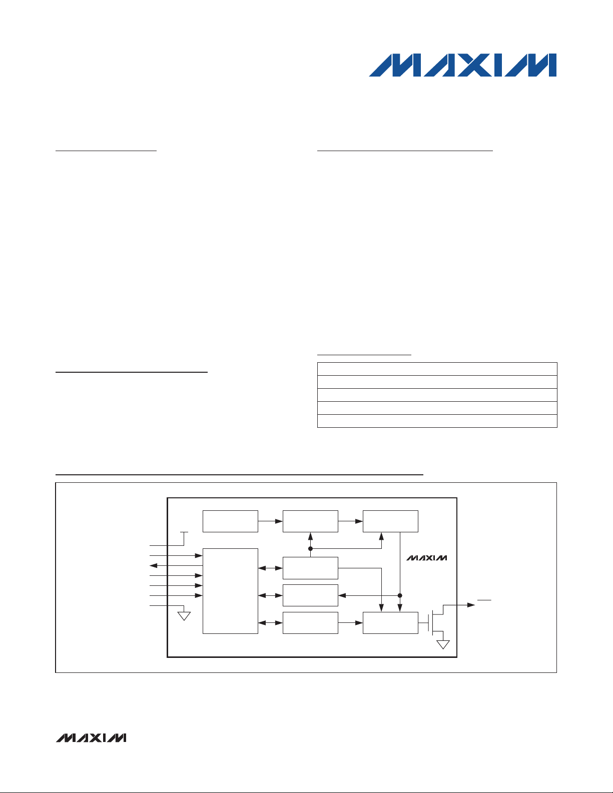
Functional Diagram
OVERSAMPLING
MODULATOR
CONFIGURATION/
STATUS REGISTER
TEMPERATURE
REGISTER
T
AND T
HIGH
LOW
REGISTERS
DIGITAL
DECIMATOR
MAX31722
MAX31723
TOUT
THERMOSTAT
COMPARATOR
V
SDI
SDO
SCLK
SERMODE
GND
PRECISION
V
DD
DD
CE
REFERENCE
I/O CONTROL
AND
INPUT SENSE
SPI is a trademark of Motorola, Inc.
µMAX is a registered trademark of Maxim Integrated Products, Inc.
_______________________________________________________________ Maxim Integrated Products 1
For pricing, delivery, and ordering information, please contact Maxim Direct at 1-888-629-4642,
or visit Maxim’s website at www.maxim-ic.com.
Page 2
Digital Thermometers and Thermostats
with SPI/3-Wire Interface
ABSOLUTE MAXIMUM RATINGS
Voltage Range on VDD Relative to GND ..............-0.3V to +6.0V
Voltage Range on Any Other Pin Relative to GND ...-0.3V to +6.0V
Continuous Power Dissipation (TA = +70NC)
FMAX (derate 4.5mW/NC above +70NC) ......................362mW
EEPROM Programming Temperature Range . ...-40NC to +85NC
Stresses beyond those listed under “Absolute Maximum Ratings” may cause permanent damage to the device. These are stress ratings only, and functional
operation of the device at these or any other conditions beyond those indicated in the operational sections of the specifications is not implied. Exposure to absolute
maximum rating conditions for extended periods may affect device reliability.
RECOMMENDED OPERATING CHARACTERISTICS
(TJ = -55NC to +125NC, unless otherwise noted.)
PARAMETER SYMBOL CONDITIONS MIN TYP MAX UNITS
Supply Voltage V
Input Logic-High V
Input Logic-Low V
MAX31722/MAX31723
DC ELECTRICAL CHARACTERISTICS
(VDD = 1.7V to 3.7V, TJ = -55NC to +125NC, unless otherwise noted.)
PARAMETER SYMBOL CONDITIONS MIN TYP MAX UNITS
MAX31722 Thermometer Error T
MAX31723 Thermometer Error T
Resolution 9 12 Bits
Conversion Time t
Logic 0 Output (SDO, TOUT)
Logic 1 Output (SDO) V
Leakage Current I
Active Current I
Shutdown Current I
DD
ERR
ERR
CONVT
V
OL
OH
CC
CC1
(Note 1) 1.7 3.7 V
(Note 1) 0.7 x V
IH
(Note 1) -0.3 0.3 x V
IL
-40NC to +85NC Q2.0
-55NC to +125NC Q3.0
0NC to +70NC Q0.5
-55NC to +125NC Q2.0
9-bit conversions 25
10-bit conversions 50
11-bit conversions 100
12-bit conversions 200
(Note 2) 0.4 V
(Note 3)
L
Active temperature conversions (Note 4) 1150
Communication only 100
EEPROM writes (-40NC to +85NC)
EEPROM writes during active temperature
conversions (-40NC to +85NC)
Operating Junction Temperature Range ......... -55NC to +125NC
Storage Temperature Range ............................ -55NC to +125NC
Lead Temperature (soldering, 10s) ................................+300NC
Soldering Temperature (reflow) ......................................+260NC
V
DD
VDD -
0.4
-1 +1
+ 0.3 V
DD
DD
1150
1200
2
V
NC
NC
ms
V
FA
FA
FA
2
Page 3
Digital Thermometers and Thermostats
with SPI/3-Wire Interface
AC ELECTRICAL CHARACTERISTICS: 3-WIRE INTERFACE
(VDD = 1.7V to 3.7V, TJ = -55NC to +125NC, unless otherwise noted.) (Figures 1, 2)
PARAMETER SYMBOL CONDITIONS MIN TYP MAX UNITS
Data to SCLK Setup t
SCLK to Data Hold t
SCLK to Data Valid t
SCLK Low Time t
SCLK High Time t
SCLK Frequency t
SCLK Rise and Fall tR, t
CE to SCLK Setup t
SCLK to CE Hold t
CE Inactive Time t
CE to Output High-Z t
SCLK to Output High-Z t
DC
CDH
CDD
CL
CH
CLK
CC
CCH
CWH
CDZ
CCZ
AC ELECTRICAL CHARACTERISTICS: SPI INTERFACE
(VDD = 1.7V to 3.7V, TJ = -55NC to +125NC, unless otherwise noted.) (Figures 3, 4)
PARAMETER SYMBOL CONDITIONS MIN TYP MAX UNITS
Data to SCLK Setup t
SCLK to Data Hold t
SCLK to Data Valid t
SCLK Low Time t
SCLK High Time t
SCLK Frequency t
SCLK Rise and Fall tR, t
CE to SCLK Setup t
SCLK to CE Hold t
CE Inactive Time t
CE to Output High-Z t
DC
CDH
CDD
CL
CH
CLK
CC
CCH
CWH
CDZ
(Notes 5, 6) 35 ns
(Notes 5, 6) 35 ns
(Notes 5, 6, 7) 80 ns
(Note 6) 100 ns
(Note 6) 100 ns
(Note 6) DC 5.0 MHz
F
(Note 6) 400 ns
(Note 6) 100 ns
(Note 6) 400 ns
(Notes 5, 6) 40 ns
(Notes 5, 6) 40 ns
(Notes 5, 6) 35 ns
(Notes 5, 6) 35 ns
(Notes 5, 6, 7) 80 ns
(Note 6) 100 ns
(Note 6) 100 ns
(Note 6) DC 5.0 MHz
F
(Note 6) 400 ns
(Note 6) 100 ns
(Note 6) 400 ns
(Notes 5, 6) 40 ns
MAX31722/MAX31723
200 ns
200 ns
AC ELECTRICAL CHARACTERISTICS: EEPROM
(VDD = 1.7V to 3.7V, TJ = -55NC to +125NC, unless otherwise noted.)
PARAMETER SYMBOL CONDITIONS MIN TYP MAX UNITS
EEPROM Write Cycle Time t
EEPROM Write Endurance N
Note 1: All voltages are referenced to ground. Currents entering the IC are specified positive, and currents exiting the IC are negative.
Note 2: Logic 0 voltages are specified at a sink current of 3mA.
Note 3: Logic 1 voltages are specified at a source current of 1mA.
Note 4: ICC specified with SCLK = VDD and CE = GND.
Note 5: Measured at VIH = 0.7V x VDD or VIL = 0.3 x VDD and 10ms maximum rise and fall times.
Note 6: Measured with 50pF load.
Note 7: Measured at VOH = 0.7 x VDD or VOL = 0.3 x VDD. Measured from the 50% point of SCLK to the VOH minimum of SDO.
Note 8: VDD must be > 2.0V during EEPROM write cycles.
WR
EEWR
-40NC to +85NC (Note 8)
-40NC P TA P +85NC (Note 8)
TA = +25NC (Note 8)
20,000
80,000
15 ms
Cycles
3
Page 4
Digital Thermometers and Thermostats
with SPI/3-Wire Interface
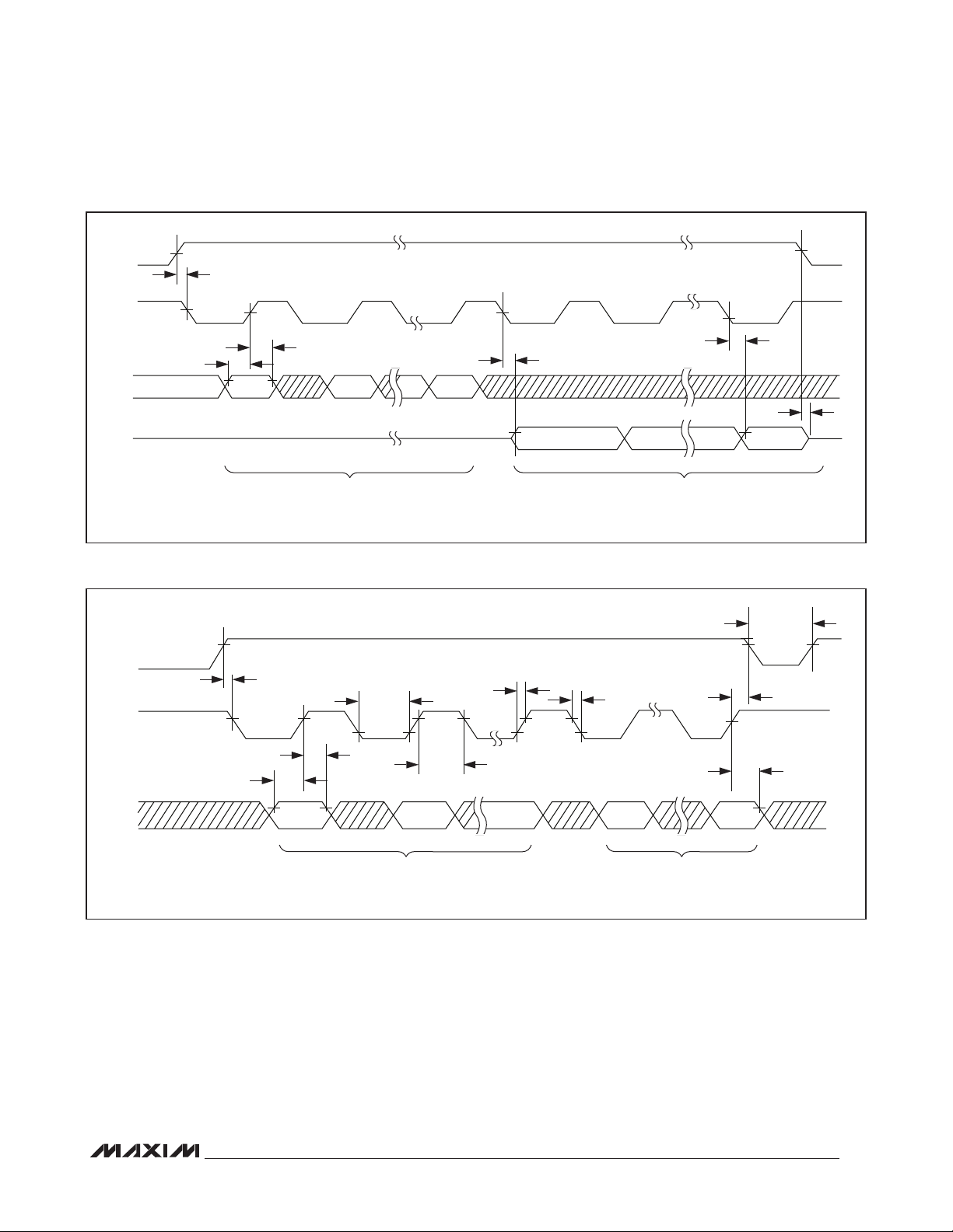
CE
SCLK
I/O*
*I/O IS SDI AND SDO CONNECTED TOGETHER.
t
CC
t
CDH
t
DC
A0 A1 A7 D0 D1
WRITE ADDRESS BYTE
Figure 1. Timing Diagram: 3-Wire Read Data Transfer
MAX31722/MAX31723
CE
t
CC
t
CL
t
CCZ
t
CDD
READ DATA BIT
t
t
R
CCH
t
F
t
t
CWH
CDD
t
CDZ
SCLK
t
CDH
t
DC
I/O*
*I/O IS SDI AND SDO CONNECTED TOGETHER.
A0 A1 A7 D0
WRITE ADDRESS BYTE WRITE DATA
Figure 2. Timing Diagram: 3-Wire Write Data Transfer
4
t
CH
Page 5
Digital Thermometers and Thermostats
with SPI/3-Wire Interface
MAX31722/MAX31723
CE
SCLK
SDI
SDO
NOTE: SCLK CAN BE EITHER POLARITY, TIMING SHOWN FOR CPOL = 1.
t
CC
t
CDH
t
DC
A7 A6 A0
WRITE ADDRESS BYTE READ DATA BYTE
Figure 3. Timing Diagram: SPI Read Data Transfer
CE
t
CC
t
t
CDD
D7 D6 D1 D0
t
t
CL
R
t
F
CDD
t
CCH
t
CDZ
t
CWH
SCLK
SDI
NOTE: SCLK CAN BE EITHER POLARITY, TIMING SHOWN FOR CPOL = 1.
t
CDH
t
DC
A7 A6 A0 D7 D0
WRITE ADDRESS BYTE WRITE DATA BYTE
Figure 4. Timing Diagram: SPI Write Data Transfer
t
CH
t
CDH
5
Page 6

Digital Thermometers and Thermostats
with SPI/3-Wire Interface
Typical Operating Characteristics
(T
= +25°C, unless otherwise noted.)
A
TEMPERATURE CONVERSION ACTIVE
SUPPLY CURRENT vs. TEMPERATURE
1200
1000
800
(µA)
600
CC
I
400
200
0
-55 125
VDD = 3.7V
VDD = 3.0V
VDD = 1.7V
105856545255-15-35
TEMPERATURE (°C)
MAX31722/MAX31723
TEMPERATURE CONVERSION ERROR
0.5
0.4
0.3
0.2
0.1
0
ERROR (°C)
-0.1
-0.2
-0.3
-0.4
-0.5
-40
1.4
1.2
MAX31722/3 toc01
(µA)
CC
I
1.0
0.8
0.6
0.4
0.2
0
vs. REFERENCE TEMPERATURE
12-BIT TEMPERATURE CONVERSIONS
TEMPERATURE (°C)
= 3.0V
V
DD
3
σ
-3
σ
STANDBY SUPPLY CURRENT
vs. TEMPERATURE
VDD = 3.7V
VDD = 3.0V
VDD = 1.7V
-55 125
TEMPERATURE (°C)
MAX31722/3 toc03
806020 400-20
85 1056545255-15-35
MAX31722/3 toc02
6
Page 7

Digital Thermometers and Thermostats
with SPI/3-Wire Interface
Pin Configuration
TOP VIEW
+
1 8 V
TOUT
2 7 SERMODECE
MAX31722
MAX31723
µMAX
Pin Description
PIN NAME FUNCTION
1
2 CE
3 SCLK
4 GND Ground. Ground connection.
5 SDO
6 SDI
7 SERMODE
8 V
TOUT
DD
Thermostat Output. Open-drain output indicator for internal thermal alarm limits.
Chip Enable. Must be asserted high for communication to take place for either the SPI or 3-wire
interfaces.
Serial-Clock Input. Used to synchronize data movement on the serial interface for either SPI or
3-wire interfaces.
Serial-Data Output. When SPI communication is selected, the SDO pin is the serial-data output for
the SPI bus. When 3-wire communication is selected, this pin must be connected to the SDI pin.
The SDI and SDO pins function as a single I/O pin when connected together.
Serial-Data Input. When SPI communication is selected, the SDI pin is the serial-data input for the
SPI bus. When 3-wire communication is selected, this pin must be connected to the SDO pin. The
SDI and SDO pins function as a single I/O pin when connected together.
Serial-Interface Mode Input. This pin selects which interface is used. When connected to VDD, SPI
communication is selected. When connected to GND, 3-wire communication is selected.
Supply Voltage. Power-supply input.
DD
SDISCLK 3 6
SDOGND 4 5
MAX31722/MAX31723
Detailed Description
The MAX31722/MAX31723 are factory-calibrated temperature sensors that require no external components.
The user can alter the configuration/status register to
place the device in a continuous temperature conversion
mode or into a one-shot conversion mode. In the continuous conversion mode, the devices continuously convert
the temperature and store the result in the temperature
register. As conversions are performed in the background, reading the temperature register does not affect
the conversion in progress. In the one-shot temperature
conversion mode, the devices perform one temperature
conversion, store the result in the temperature register,
and then return to the shutdown state. This conversion
mode is ideal for power-sensitive applications. The
temperature conversion results have a default resolution
of 9 bits. In applications where small incremental temperature changes are critical, the user can change the
conversion resolution from 9 bits to 10, 11, or 12. This is
accomplished by programming the configuration/status
register.
The devices can be configured as a thermostat, allowing for the TOUT pin to behave as an interrupt, triggering when the programmed limits, T
HIGH
and T
LOW
, are
surpassed. The devices can communicate using either a
serial peripheral interface (SPI) or standard 3-wire interface. The user can select either communication standard
through the SERMODE pin, connecting it to V
DD
for SPI
and to GND for 3-wire.
7
Page 8

Digital Thermometers and Thermostats
with SPI/3-Wire Interface
Measuring Temperature
The core of the devices’ functionality is its direct-to-digital
temperature sensor. The devices measure temperature
through the use of an on-chip temperature measurement technique with a -55NC to +125NC operating range.
The devices power up in a power-conserving shutdown
mode. After power-up, the devices can be placed in a
continuous conversion mode or in a one-shot conversion mode. In the continuous conversion mode, the
devices continuously compute the temperature and
store the most recent result in the temperature register at
addresses 01h (LSB) and 02h (MSB). As conversions are
performed in the background, reading the temperature
register does not affect the conversion in progress. The
temperature value is not updated until the SPI or 3-wire
interface is inactive. In other words, CE must be inactive
for the temperature register to be updated with the most
recent temperature conversion value. In the one-shot
conversion mode, the devices perform one temperature
MAX31722/MAX31723
conversion and then return to the shutdown mode, storing
temperature in the temperature register. This conversion
S 2
MSB
-1
2
6
-2
2
5
2
-3
2
4
2
-4
2
mode is ideal for power-sensitive applications. Details on
how to change the setting after power-up are contained
in the Programming section.
The resolution of the temperature conversion is configurable (9, 10, 11, or 12 bits) with 9 bits reading the
default state. This equates to a temperature resolution
of 0.5NC, 0.25NC, 0.125NC, or 0.0625NC. Following each
conversion, thermal data is stored in the temperature
register in two’s complement format. The information
can be retrieved over the SPI or 3-wire interface with the
address set to the temperature register, 01h (LSB) and
then 02h (MSB). Table 1 describes the exact relationship of output data to measured temperature. Table 1
assumes the devices are configured for 12-bit resolution.
If the devices are configured in a lower resolution mode,
those bits contain zeros. The data is transmitted serially
over the digital interface, MSB first for SPI communication and LSB first for 3-wire communication. The MSB of
the temperature register contains the sign (S) bit, denoting whether the temperature is positive or negative.
3
2
(UNITS = NC)
0 0 0 0 01h
2
2
1
2
2
LSB
0
02h
Figure 5. Temperature, T
HIGH
, and T
Register Format
LOW
Table 1. 12-Bit Resolution Temperature/Data Relationship
TEMPERATURE
(NC)
+125 0111 1101 0000 0000 7D00
+25.0625 0001 1001 0001 0000 1910
+10.125 0000 1010 0010 0000 0A20
+0.5 0000 0000 1000 0000 0080
0 0000 0000 0000 0000 0000
-0.5 1111 1111 1000 0000 FF80
-10.125 1111 0101 1110 0000 F5E0
-25.0625 1110 0110 1111 0000 E6F0
-55 1100 1001 0000 0000 C900
8
DIGITAL OUTPUT
(BINARY)
DIGITAL OUTPUT
(HEX)
Page 9

Digital Thermometers and Thermostats
Thermostat
The devices’ thermostat can be programmed to power
up in either comparator mode or interrupt mode, which
activate and deactivate the open-drain thermostat output
(TOUT) based on user-programmable trip points (T
and T
LOW
). The T
HIGH
and T
registers contain
LOW
Celsius temperature values in two’s complement format
and are stored in EEPROM memory. As such, the values
are nonvolatile and can be programmed prior to installing the devices for stand-alone operation.
The data format of the T
HIGH
and T
registers is
LOW
identical to that of the temperature register (Figure 5).
After every temperature conversion, the measurement is
compared to the values stored in the T
registers. The T
register is assigned to address
HIGH
HIGH
locations 03h (LSB) and 04h (MSB), and the T
ister is assigned to address locations 05h (LSB) and
06h (MSB). The TOUT output is updated based on the
result of the comparison and the operating mode of the
devices. The number of T
HIGH
and T
bits used dur-
LOW
ing the thermostat comparison is equal to the conversion
resolution set by the R1 and R0 bits in the configuration/
status register. For example, if the resolution is 9 bits,
only the nine MSBs of T
HIGH
and T
are used by the
LOW
thermostat comparator.
and T
LOW
HIGH
LOW
reg-
with SPI/3-Wire Interface
If the user does not wish to use the thermostat capabilities of the devices, the TOUT output should be left
unconnected. Note that if the thermostat is not used, the
T
and T
HIGH
age of system data.
When the thermostat is in comparator mode, TOUT
can be programmed to operate with any amount of
hysteresis. The TOUT output becomes active when the
measured temperature exceeds the T
then stays active until the first time the temperature falls
below the value stored in T
shutdown mode does not clear TOUT in comparator
mode. Figure 6 illustrates thermostat comparator mode
operation.
In interrupt mode, the TOUT output first becomes active
when the measured temperature exceeds the T
value. Once activated, in continuous conversion mode
TOUT can only be cleared by either putting the devices
into shutdown mode or by reading from any register
(configuration/status, temperature, T
on the devices. In one-shot mode, TOUT can only be
cleared by reading from any register (configuration/
status, temperature, T
registers can be used for general stor-
LOW
Comparator Mode
value. TOUT
HIGH
. Putting the devices into
LOW
Interrupt Mode
, or T
HIGH
HIGH
, or T
) on the devices.
LOW
HIGH
LOW
MAX31722/MAX31723
)
TEMPERATURE
TOUT OUTPUT—COMPARATOR MODE
TOUT OUTPUT—INTERRUPT MODE
Figure 6. TOUT Operation Example
T
HIGH
T
LOW
INACTIVE
ACTIVE
INACTIVE
ACTIVE
ASSUMES A READ
HAS OCCURED
CONVERSIONS
9
Page 10

Digital Thermometers and Thermostats
with SPI/3-Wire Interface
In either mode, once TOUT has been deactivated, it is
only reactivated when the measured temperature falls
below the T
cess is cyclical between T
T
, clear, T
HIGH
value. Thus, this interrupt/clear pro-
LOW
LOW
HIGH
, clear, T
and T
HIGH
, clear, T
events (i.e,
LOW
LOW
etc.). Figure 6 illustrates the thermostat interrupt mode
operation.
Table 2. Register Address Structure
READ
ADDRESS
(HEX)
00 80 Configuration/Status
01 No access Temperature LSB
02 No access Temperature MSB
03 83 T
04 84 T
MAX31722/MAX31723
05 85 T
06 86 T
WRITE
ADDRESS
(HEX)
ACTIVE REGISTER
LSB
HIGH
MSB
HIGH
LSB
LOW
MSB
LOW
, clear,
Programming
The area of interest in programming the devices is the
configuration/status register. All programming is done
through the SPI or 3-wire communication interface by
selecting the appropriate address of the desired register
location. Table 2 illustrates the addresses for the device
registers.
Configuration/Status Register Programming
The configuration/status register is accessed in the
devices with the 00h address for reads and the 80h
address for writes. Data is read from or written to the
configuration/status register MSB first for SPI communication and LSB first for 3-wire communication. Table 3
illustrates the format of the register, describes the effect
each bit has on device functionality, and provides the
bit’s factory state.
Table 4 defines the resolution of the digital thermometer,
based on the settings of the R1 and R0 bits. There is a
direct trade-off between resolution and conversion time,
Table 3. Configuration/Status Register Bit Descriptions
BIT 7 BIT 6 BIT 5 BIT 4 BIT 3 BIT 2 BIT 1 BIT 0
0 MEMW NVB 1SHOT TM R1 R0 SD
BIT 7 This bit is always a value of 0.
MEMW: Memory write bit. Power-up state = 0. The user has read/write access to the MEMW bit, which is
stored in the voltage memory.
0 = A write of the configuration/status register is stored in RAM memory.
BIT 6
BIT 5
BIT 4
BIT 3
10
1 = A write of the configuration/status register is stored in EEPROM.
Note: The status of this bit is ignored if a EEPROM write occurs to the other nonvolatile registers, T
T
. The nonvolatile bits of the configuration/status register are written if a EEPROM write cycle occurs to the
LOW
T
and T
HIGH
NVB: Nonvolatile memory busy flag. Power-up state = 0 and is stored in volatile memory.
0 = Indicates that the nonvolatile memory is not busy.
1 = Indicates there is a write to a EEPROM memory cell in progress.
1SHOT: One-shot temperature conversion bit. Power-up state = 0 and is stored in volatile memory.
0 = Disables 1SHOT mode.
1 = If the SD bit is 1 (continuous temperature conversions are not taking place), a 1 written to the 1SHOT bit
causes the devices to perform one temperature conversion and store the results in the temperature register
at addresses 01h (LSB) and 02h (MSB). The bit clears itself to 0 upon completion of the temperature conversion. The user has read/write access to the 1SHOT bit, although writes to this bit are ignored if the SD bit is a 0
(continuous conversion mode).
TM: Thermostat operating mode. Factory power-up state = 0. The user has read/write access to the TM bit,
which is stored in nonvolatile memory.
0 = The thermostat output is in comparator mode.
1 = The thermostat output is in interrupt mode.
LOW
registers.
HIGH
and
Page 11

Digital Thermometers and Thermostats
with SPI/3-Wire Interface
Table 3. Configuration/Status Register Bit Descriptions (continued)
BIT 2
BIT 1
BIT 0
R1: Thermostat resolution bit 1. Factory power-up state = 0 and is stored in nonvolatile memory. Sets the conversion resolution (see Table 4).
R0: Thermostat resolution bit 0. Factory power-up state = 0 and is stored in nonvolatile memory. Sets the conversion resolution (see Table 4).
SD: Factory power-up state = 1. The user has read/write access to the SD bit, which is stored in nonvolatile
memory.
0 = The devices continuously perform temperature conversions and store the last completed result in the temperature register.
1 = The conversion in progress is completed and stored, and then the devices revert to a low-power shutdown
mode. The communication port remains active.
MAX31722/MAX31723
Table 4. Thermometer Resolution
Configuration
R1 R0
0 0 9 25
0 1 10 50
1 0 11 100
1 1 12 200
as depicted in the AC Electrical Characteristics. The user
has read/write access to the R1 and R0 bits, which are
nonvolatile. See Table 4.
THERMOMETER
RESOLUTION (BITS)
MAX CONVERSION
TIME (ms)
Serial Interface
The devices offer the flexibility to choose between two
serial interface modes. They can communicate with the
SPI interface or with a 3-wire interface. The interface
method used is determined by the SERMODE pin. When
SERMODE is connected to VDD, SPI communication
is selected. When SERMODE is connected to ground,
3-wire communication is selected.
Table 5. Function Table
MODE CE SCLK SDI SDO
Disable reset Low Input disabled Input disabled High impedance
Write High
Read High
Note: CPHA bit polarity must be set to 1.
*CPOL is the clock polarity bit that is set in the control register of the microcontroller.
**SDO remains at high impedance until 8 bits of data are ready to be shifted out during a read.
CPOL = 1*, SCLK rising
CPOL = 0, SCLK falling
CPOL = 1, SCLK falling
CPOL = 0, SCLK rising
The SPI is a synchronous bus for address and data
transfer. The SPI mode of serial communication is selected by connecting SERMODE to VDD. Four pins are used
for the SPI: SDO (serial-data out), SDI (serial-data in), CE
(chip enable), and SCLK (serial clock). The devices are
the slave device in an SPI application, with the microcontroller being the master. SDI and SDO are the serial-data
input and output pins for the devices, respectively. The
CE input is used to initiate and terminate a data transfer.
SCLK is used to synchronize data movement between
the master (microcontroller) and the slave (IC) devices.
The serial clock (SCLK), which is generated by the
microcontroller, is active only when CE is high and during address and data transfer to any device on the SPI
bus. The inactive clock polarity is programmable in some
microcontrollers. The devices offer an important feature
in that the level of the inactive clock is determined by
sampling SCLK when CE becomes active. Therefore,
either SCLK polarity can be accommodated. Input data
(SDI) is latched on the internal strobe edge and output
data (SDO) is shifted out on the shift edge (see Table 5
and Figure 7). There is one clock for each bit transferred.
Address and data bits are transferred in groups of eight,
MSB first.
Serial Peripheral Interface (SPI)
Data bit latch High impedance
X Next data bit shift**
11
Page 12

Digital Thermometers and Thermostats
with SPI/3-Wire Interface
CPOL = 1
CPOL = 0
Figure 7. Serial Clock as a Function of Microcontroller Clock Polarity (CPOL)
CE
SCLK
CE
SCLK
NOTE: CPOL IS A BIT THAT IS SET IN THE MICROCONTROLLER’S CONTROL REGISTER.
Address and Data Bytes
Address and data bytes are shifted MSB first into the
serial-data input (SDI) and out of the serial-data output
MAX31722/MAX31723
(SDO). Any transfer requires the address of the byte to
specify a write or a read, followed by one or more bytes of
data. Data is transferred out of the SDO for a read operation and into the SDI for a write operation. The address
byte is always the first byte entered after CE is driven
high. The MSB (A7) of this byte determines if a read or
write takes place. If A7 is 0, one or more read cycles
occur. If A7 is 1, one or more write cycles occur.
Data transfers can occur 1 byte at a time in multiple-byte
burst mode. After CE is driven high, an address is written to the devices. After the address, one or more data
bytes can be written or read. For a single-byte transfer,
1 byte is read or written and then CE is driven low (see
Figures 8 and 9). For a multiple-byte transfer, however,
multiple bytes can be read or written to the devices
after the address has been written (see Figure 10). A
SHIFT
SHIFT INTERNAL STROBE
single-byte burst read/write sequentially points through
all memory locations and loops from 7Fh/FFh to 00h/80h.
Invalid memory addresses report an FFh value.
INTERNAL STROBE
3-Wire Serial-Data Bus
The 3-wire communication mode operates similarly to
the SPI mode. However, in 3-wire mode, there is one
bidirectional I/O instead of separate data-in and dataout signals. The 3-wire consists of the I/O (SDI and
SDO pins connected together), CE, and SCLK pins. In
3-wire mode, each byte is shifted in LSB first, unlike SPI
mode where each byte is shifted in MSB first. As is the
case with the SPI mode, an address byte is written to
the devices followed by a single data byte or multiple
data bytes. Figure 11 illustrates a read and write cycle.
Figure 12 illustrates a multiple-byte burst transfer. In
3-wire mode, data is input on the rising edge of SCLK
and output on the falling edge of SCLK.
12
Page 13

CE
SCLK
SDI
Digital Thermometers and Thermostats
with SPI/3-Wire Interface
A7
A6 A5 A4 A3 A2 A1 A0
MAX31722/MAX31723
SDO HIGH-Z
Figure 8. SPI Single-Byte Read
CE
SCLK
SDI
A7
A6 A5 A4 A3 A2 A1 A0 D7 D6 D5 D4 D3 D2 D1 D0
SDO HIGH-Z
Figure 9. SPI Single-Byte Write
CE
SCLK
D7 D6 D5 D4 D3 D2 D1 D0
SDIWRITE
SDI
READ
SDO
Figure 10. SPI Multiple-Byte Burst Transfer
ADDRESS
BYTE
ADDRESS
BYTE
DATA
BYTE 0
DATA
BYTE 0
DATA
BYTE 1
DATA
BYTE 1
DATA
BYTE N
DATA
BYTE N
13
Page 14

Digital Thermometers and Thermostats
with SPI/3-Wire Interface
CE
SCLK
I/O*
*I/O IS SDI AND SDO CONNECTED TOGETHER.
Figure 11. 3-Wire Single-Byte Transfer
MAX31722/MAX31723
Figure 12. 3-Wire Multiple-Byte Burst Transfer
A0 A1 A2 A3 A4 A5 A6 A7 D0 D1 D2 D3 D4 D5 D6 D7
CE
SCLK
I/O*
*I/O IS SDI AND SDO CONNECTED TOGETHER.
ADDRESS
BYTE
DATA
BYTE 0
DATA
BYTE 1
DATA
BYTE N
Package Information
For the latest package outline information and land patterns, go to www.maxim-ic.com/packages. Note that a “+”, “#”, or “-” in the
package code indicates RoHS status only. Package drawings may show a different suffix character, but the drawing pertains to the
package regardless of RoHS status.
PACKAGE TYPE PACKAGE CODE OUTLINE NO. LAND PATTERN NO.
8 FMAX
U8+1
21-0036 90-0092
14
Page 15

Digital Thermometers and Thermostats
with SPI/3-Wire Interface
Revision History
MAX31722/MAX31723
REVISION
NUMBER
0 11/10 Initial release —
REVISION
DATE
DESCRIPTION
PAGES
CHANGED
Maxim cannot assume responsibility for use of any circuitry other than circuitry entirely embodied in a Maxim product. No circuit patent licenses are implied.
Maxim reserves the right to change the circuitry and specifications without notice at any time.
Maxim Integrated Products, 120 San Gabriel Drive, Sunnyvale, CA 94086 408-737-7600 15
©
2010 Maxim Integrated Products Maxim is a registered trademark of Maxim Integrated Products, Inc.
 Loading...