

Page 1
General Description
The MAX3030E–MAX3033E family of quad RS-422
transmitters send digital data transmission signals over
twisted-pair balanced lines in accordance with TIA/EIA422-B and ITU-T V.11 standards. All transmitter outputs
are protected to ±15kV using the Human Body Model.
The MAX3030E–MAX3033E are available with either a
2Mbps or 20Mbps guaranteed baud rate. The 2Mbps
baud rate transmitters feature slew-rate-limiting to minimize EMI and reduce reflections caused by improperly
terminated cables.
The 20Mbps baud rate transmitters feature low-static
current consumption (ICC< 100µA), making them ideal
for battery-powered and power-conscious applications.
They have a maximum propagation delay of 16ns and a
part-to-part skew less than 5ns, making these devices
ideal for driving parallel data. The MAX3030E–
MAX3033E feature hot-swap capability that eliminates
false transitions on the data cable during power-up or
hot insertion.
The MAX3030E–MAX3033E are low-power, ESD-protected, pin-compatible upgrades to the industry-standard 26LS31 and SN75174. They are available in
space-saving 16-pin TSSOP and SO packages.
Applications
Telecom Backplanes
V.11/X.21 Interface
Industrial PLCs
Motor Control
Features
♦ Meet TIA/EIA-422-B (RS-422) and ITU-T V.11
Recommendation
♦ ±15kV ESD Protection on Tx Outputs
♦ Hot-Swap Functionality
♦ Guaranteed 20Mbps Data Rate (MAX3030E,
MAX3032E)
♦ Slew-Rate-Controlled 2Mbps Data Rate
(MAX3031E, MAX3033E)
♦ Available in 16-Pin TSSOP and Narrow SO
Packages
♦ Low-Power Design (<330µW, V
CC
= 3.3V Static)
♦ +3.3V Operation
♦ Industry-Standard Pinout
♦ Thermal Shutdown
MAX3030E–MAX3033E
±15kV ESD-Protected, 3.3V Quad
RS-422 Transmitters
________________________________________________________________ Maxim Integrated Products 1
Ordering Information
19-2671; Rev 0; 10/02
For pricing, delivery, and ordering information, please contact Maxim/Dallas Direct! at
1-888-629-4642, or visit Maxim’s website at www.maxim-ic.com.
Pin Configurations
TOP VIEW
DI1
1
DO1+
2
DO1-
3
MAX3030E/
4
EN
DI2
5
6
7
8
MAX3031E
TSSOP/SO
DO2-
DO2+
GND
DO1+
DO1-
EN1&2
DO2-
DO2+
GND
DI1
DI2
1
2
3
4
5
6
7
8
MAX3032E/
MAX3033E
TSSOP/SO
16
V
CC
DI4
15
DO4+
14
DO4-
13
12
EN
DO3-
11
DO3+
10
DI3
9
PART TEMP RANGE PIN-PACKAGE
MAX3030ECSE 0°C to +70°C 16 SO (Narrow)
MAX3030ECUE 0°C to +70°C 16 TSSOP
MAX3030EESE -40°C to +85°C 16 SO (Narrow)
MAX3030EEUE -40°C to +85°C 16 TSSOP
MAX3031ECSE 0°C to +70°C 16 SO (Narrow)
MAX3031ECUE 0°C to +70°C 16 TSSOP
MAX3031EESE -40°C to +85°C 16 SO (Narrow)
MAX3031EEUE -40°C to +85°C 16 TSSOP
16
V
CC
DI4
15
DO4+
14
DO4-
13
12
EN3&4
DO3-
11
DO3+
10
DI3
9
MAX3032ECSE 0°C to +70°C 16 SO (Narrow)
MAX3032ECUE 0°C to +70°C 16 TSSOP
MAX3032EESE -40°C to +85°C 16 SO (Narrow)
MAX3032EEUE -40°C to +85°C 16 TSSOP
MAX3033ECSE 0°C to +70°C 16 SO (Narrow)
MAX3033ECUE 0°C to +70°C 16 TSSOP
MAX3033EESE -40°C to +85°C 16 SO (Narrow)
MAX3033EEUE -40°C to +85°C 16 TSSOP
Page 2

MAX3030E–MAX3033E
±15kV ESD-Protected, 3.3V Quad
RS-422 Transmitters
2 _______________________________________________________________________________________
ABSOLUTE MAXIMUM RATINGS
DC ELECTRICAL CHARACTERISTICS
(3V ≤ VCC≤ 3.6V, TA= T
MIN
to T
MAX
, unless otherwise noted. Typical values are at VCC= +3.3V and TA= +25°C.) (Note 1)
Stresses beyond those listed under “Absolute Maximum Ratings” may cause permanent damage to the device. These are stress ratings only, and functional
operation of the device at these or any other conditions beyond those indicated in the operational sections of the specifications is not implied. Exposure to
absolute maximum rating conditions for extended periods may affect device reliability.
(All Voltages Are Referenced to Device Ground, Unless
Otherwise Noted)
VCC........................................................................................+6V
EN1&2, EN3&4, EN, EN............................................-0.3V to +6V
DI_ ............................................................................-0.3V to +6V
DO_+, DO_- (normal condition) .................-0.3V to (V
CC
+ 0.3V)
DO_+, DO_- (power-off or three-state condition).....-0.3V to +6V
Driver Output Current per Pin.........................................±150mA
Continuous Power Dissipation (T
A
= +70°C)
16-Pin SO (derate 8.70mW/°C above +70°C)..............696mW
16-Pin TSSOP (derate 9.40mW/°C above +70°C) .......755mW
Operating Temperature Ranges
MAX303_EC_ ......................................................0°C to +70°C
MAX303_EE_ ...................................................-40°C to +85°C
Junction Temperature......................................................+150°C
Storage Temperature Range .............................-65°C to +160°C
Lead Temperature (soldering, 10s) .................................+300°C
DRIVER OUTPUT: DO_+, DO_-
Differential Driver Output
Change in Differential Output
Voltage
Driver Common-Mode Output
Voltage
Change in Common-Mode
Voltage
Three-State Leakage Current I
Output Leakage Current I
Driver Output Short-Circuit
Current
INPUTS: EN, EN, EN1&2, EN3&4
Input High Voltage V
Input Low Voltage V
Input Current I
Hot-Swap Driver Input Current I
SUPPLY CURRENT
Supply Current I
THERMAL PROTECTION
Thermal-Shutdown Threshold T
Thermal-Shutdown Hysteresis 10 °C
ESD Protection DO_ Human Body Model ±15 kV
PARAMETER SYMBOL CONDITIONS MIN TYP MAX UNITS
V
OD1
V
OD2
V
OD3
∆V
V
OC
∆V
OZ
OFF
I
SC
LEAK
HOTSWAP
CC
SH
RL = 100Ω, Figure 1 2.0
RL = ∞, Figure 1 3.6
RL = 3.9kΩ (for compliance with V.11),
Figure 1
RL = 100Ω (Note 2) -0.4 +0.4 V
OD
RL = 100Ω, Figure 1 3 V
RL = 100Ω (Note 2) -0.4 +0.4 V
OC
V
= VCC or GND, driver disabled ±10 µA
OUT
VCC = 0V, V
V
= 0V, VIN = VCC or GND
OUT
(Note 3)
IH
IL
EN, EN, EN1&2, EN3&4 (Note 4) ±200 µA
No load 100 µA
= 3V or 6V 20 µA
OUT
3.6
-150 mA
2.0 V
0.4 V
±2 µA
160 °C
V
Page 3

MAX3030E–MAX3033E
±15kV ESD-Protected, 3.3V Quad
RS-422 Transmitters
_______________________________________________________________________________________ 3
SWITCHING CHARACTERISTICS—MAX3030E, MAX3032E
(3V ≤ VCC≤ 3.6V, TA= T
MIN
to T
MAX
, unless otherwise noted. Typical values are at VCC= +3.3V and TA= +25°C.)
SWITCHING CHARACTERISTICS—MAX3031E, MAX3033E
(3V ≤ VCC≤ 3.6V, TA= T
MIN
to T
MAX
, unless otherwise noted. Typical values are at VCC= +3.3V and TA= +25°C.)
Driver Propagation Delay
Low to High
Driver Propagation Delay
High to Low
Differential Transition Time, Low
to High
Differential Transition Time, High
to Low
Differential Skew (Same Channel)
|t
DPLH
Skew Driver to Driver
(Same Device)
Skew Part to Part t
Maximum Data Rate 20 Mbps
Driver Enable to Output High t
Driver Enable to Output Low t
Driver Disable Time from Low t
Driver Disable Time from High t
PARAMETER SYMBOL CONDITIONS MIN TYP MAX UNITS
- t
|
DPHL
t
DPLH
RL = 100Ω, CL = 50pF, Figures 2, 3 8 16 ns
t
DPHL
t
R
RL = 100Ω, CL = 50pF (10% to 90%),
t
t
SK1
t
SK2
SK3
DZH
DZL
DLZ
DHZ
Figures 2, 3
F
RL = 100Ω, CL = 50pF, VCC = 3.3V ±2 ns
RL = 100Ω, CL = 50pF, VCC = 3.3V,
MAX
=
+5°C
∆T
S2 closed, RL = 500Ω, CL = 50pF,
Figures 4, 5
S1 closed, RL = 500Ω, CL = 50pF,
Figures 4, 5
S1 closed, RL = 500Ω, CL = 50pF,
Figures 4, 5
S2 closed, RL = 500Ω, CL = 50pF,
Figures 4, 5
10 ns
5ns
50 ns
50 ns
50 ns
50 ns
Driver Propagation Delay
Low to High
Driver Propagation Delay
High to Low
Differential Transition Time,
Low to High
Differential Transition Time,
High to Low
Differential Skew (Same Channel)
|t
DPLH
Skew Driver to Driver
(Same Device)
PARAMETER SYMBOL CONDITIONS MIN TYP MAX UNITS
- t
|
DPHL
t
DPLH
RL = 100Ω, CL = 50pF, Figures 2, 3 40 70 ns
t
DPHL
t
R
RL = 100Ω, CL = 50pF (10% to 90%),
Figures 2, 3
F
RL = 100Ω, CL = 50pF, VCC = 3.3V ±10 ns
t
SK1
t
SK2
t
15 50 ns
Page 4

MAX3030E–MAX3033E
±15kV ESD-Protected, 3.3V Quad
RS-422 Transmitters
4 _______________________________________________________________________________________
SWITCHING CHARACTERISTICS—MAX3031E, MAX3033E (continued)
(3V ≤ VCC≤ 3.6V, TA= T
MIN
to T
MAX
, unless otherwise noted. Typical values are at VCC= +3.3V and TA= +25°C.)
Note 1: All currents into the device are positive; all currents out of the device are negative. All voltages are referenced to device
ground, unless otherwise noted.
Note 2: ∆V
OD
and ∆VOCare the changes in VODand VOC, respectively, when DI changes state.
Note 3: Only one output shorted at a time.
Note 4: This input current is for the hot-swap enable (EN_, EN, EN) inputs and is present until the first transition only. After the first
transition, the input reverts to a standard high-impedance CMOS input with input current I
LEAK
.
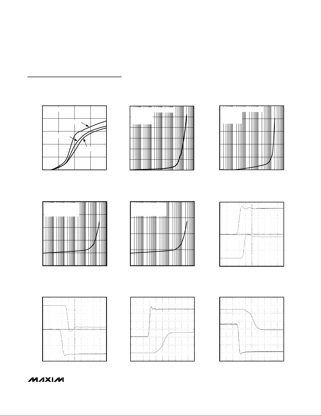
DIFFERENTIAL OUTPUT VOLTAGE
vs. OUTPUT CURRENT
MAX3030E toc01
OUTPUT CURRENT (mA)
DIFFERENTIAL OUTPUT VOLTAGE (V)
906030
1
2
3
4
0
0 120
TA = 0°C
TA = +25°C
TA = +85°C
OUTPUT CURRENT
vs. TRANSMITTER OUTPUT LOW VOLTAGE
MAX3030E toc02
OUTPUT LOW VOLTAGE (V)
OUTPUT CURRENT (mA)
321
50
100
150
200
0
04
OUTPUT CURRENT
vs. TRANSMITTER OUTPUT HIGH VOLTAGE
MAX3030E toc03
OUTPUT HIGH VOLTAGE (V)
OUTPUT CURRENT (mA)
321
25
50
75
100
125
150
0
04
Typical Operating Characteristics
(VCC= +3.3V and TA= +25°C, unless otherwise noted.)
PARAMETER SYMBOL CONDITIONS MIN TYP MAX UNITS
Skew Part to Part t
Maximum Data Rate 2 Mbps
Driver Enable to Output High t
Driver Enable to Output Low t
Driver Disable Time from Low t
Driver Disable Time from High t
SK3
DZH
DZL
DLZ
DHZ
RL = 100Ω, CL = 50pF, VCC = 3.3V,
MAX
=
+5°C
∆T
S2 closed, RL = 500Ω, CL = 50pF,
Figures 4, 5
S1 closed, RL = 500Ω, CL = 50pF,
Figures 4, 5
S1 closed, RL = 500Ω, CL = 50pF,
Figures 4, 5
S2 closed, RL = 500Ω, CL = 50pF,
Figures 4, 5
18 ns
100 ns
100 ns
150 ns
150 ns
Page 5
MAX3030E–MAX3033E
±15kV ESD-Protected, 3.3V Quad
RS-422 Transmitters
_______________________________________________________________________________________ 5
L
L
Typical Operating Characteristics (continued)
(VCC= +3.3V and TA= +25°C, unless otherwise noted.)
SUPPLY CURRENT
100
DRIVERS ENABLED
80
60
40
SUPPLY CURRENT (µA)
20
0
04
TA = +85°C
TA = +25°C
TA = 0°C
321
SUPPLY VOLTAGE (V)
MAX3030E toc04
MAX3030E/MAX3032E
SUPPLY CURRENT vs. DATA RATE
130
ALL FOUR TRANSMITTERS
LOADED AND SWITCHING
= 100Ω, CL = 200pF
R
vs. SUPPLY VOLTAGE
L
120
110
100
SUPPLY CURRENT (mA)
90
MAX3030E toc07
SUPPLY CURRENT vs. DATA RATE
30
NO RESISTIVE LOAD, CL = 200pF,
ALL FOUR
25
TRANSMITTERS
SWITCHING
20
15
10
SUPPLY CURRENT (mA)
5
0
0.1k 100M
SUPPLY CURRENT vs. DATA RATE
100
ALL FOUR TRANSMITTERS
LOADED AND SWITCHING
= 100Ω, CL = 200pF
R
L
97
94
SUPPLY CURRENT (mA)
91
MAX3030E/MAX3032E
DATA RATE (bps)
MAX3031E/MAX3033E
MAX3031E/MAX3033E
SUPPLY CURRENT vs. DATA RATE
2.5
NO RESISTIVE LOAD, CL = 200pF,
ALL FOUR
TRANSMITTERS
MAX3030E toc05
10M1M100k10k1k
2.0
SWITCHING
1.5
1.0
SUPPLY CURRENT (mA)
0.5
0
0.1k 10M
DATA RATE (bps)
1M100k10k1k
MAX3030E
DRIVER PROPAGATION DELAY
(LOW TO HIGH)
MAX3030E toc08
MAX3030E toc09
MAX3030E toc06
DI_
1V/div
DIFFERENTIA
OUTPUT
2V/div
80
0.1k 100M
DATA RATE (bps)
10M1M100k10k1k
MAX3030E
DRIVER PROPAGATION DELAY
(HIGH TO LOW)
10ns/div
MAX3030E toc10
DIFFERENTIAL
OUTPUT
2V/div
DI_
1V/div
88
0.1k 10M
DATA RATE (bps)
1M100k10k1k
MAX3031E
DRIVER PROPAGATION DELAY
(LOW TO HIGH)
20ns/div
MAX3030E toc11
DI_
1V/div
DIFFERENTIAL
OUTPUT
2V/div
10ns/div
MAX3031E
DRIVER PROPAGATION DELAY
(HIGH TO LOW)
20ns/div
MAX3030E toc12
DIFFERENTIA
OUTPUT
2V/div
DI_
1V/div
Page 6

MAX3030E–MAX3033E
±15kV ESD-Protected, 3.3V Quad
RS-422 Transmitters
6 _______________________________________________________________________________________
Pin Description
ENABLE RESPONSE TIME
MAX3030E toc13
20ns/div
ENABLE
1V/div
DIFFERENTIAL
OUTPUT
2V/div
MAX3033E EYE DIAGRAM
MAX3030E toc14
100ns/div
DO_+
1V/div
DO_1V/div
Typical Operating Characteristics (continued)
(VCC= +3.3V and TA= +25°C, unless otherwise noted.)
MAX3030E/
MAX3031E
1, 7, 9, 15 1, 7, 9, 15
2, 6, 10, 14 2, 6, 10, 14
3, 5, 11, 13 3, 5, 11, 13
PIN
MAX3032E/
MAX3033E
4 — EN
8 8 GND Ground
12 — EN
— 4 EN1&2
— 12 EN3&4
16 16 V
NAME FUNCTION
DI1, DI2,
DI3, DI4
DO1+, DO2+,
DO3+, DO4+
DO1-, DO2-,
DO3-, DO4-
CC
Transmitter Inputs. When the corresponding transmitter is enabled, a low on DI_ forces
the noninverting output low and inverting output high. Similarly, a high on DI_ forces
noninverting output high and inverting output low.
Noninverting RS-422 Outputs
Inverting RS-422 Outputs
Transmitter Enable Input: Active HIGH. Drive EN HIGH to enable all transmitters. When
EN is HIGH, drive EN LOW to disable (three-state) all the transmitters. The transmitter
outputs are high impedance when disabled. EN is hot-swap protected (see the Hot
Swap section).
Transmitter Enable Input: Active LOW. Drive EN LOW to enable all transmitters. When
EN is LOW, drive EN HIGH to disable all the transmitters. The transmitter outputs are
high impedance when disabled. EN is hot-swap protected (see the Hot Swap section).
Transmitter Enable Input for Channels 1 and 2. Drive EN1&2 HIGH to enable the
corresponding transmitters. Drive EN1&2 LOW to disable the corresponding
transmitters. The transmitter outputs are high impedance when disabled. EN1&2 is hotswap protected (see the Hot Swap section).
Transmitter Enable Input for Channels 3 and 4. Drive EN3&4 HIGH to enable the
corresponding transmitters. Drive EN3&4 LOW to disable the corresponding
transmitters. The transmitter outputs are high impedance when disabled. EN3&4 is hotswap protected (see the Hot Swap section).
Positive Supply; +3V ≤ V
≤ +3.6V. Bypass VCC to GND with a 0.1µF capacitor.
CC
Page 7

MAX3030E–MAX3033E
±15kV ESD-Protected, 3.3V Quad
RS-422 Transmitters
_______________________________________________________________________________________ 7
Test Circuits and Timing Diagrams
Figure 2. Differential Driver Propagation Delay and Transition
Time Test Circuit
Figure 1. Differential Driver DC Test Circuit
Figure 4. Driver Enable/Disable Delays Test Circuit
Figure 3. Differential Driver Propagation Delay and Transition
Waveform
Figure 5. Driver Enable/Disable Waveform
Figure 6. Short-Circuit Measurements
DI_+
R
L
2
V
OD
R
L
2
DI_-
3V
DI
V
DIFF
1.5V 1.5V
DO_-
DO_+
-V
0V
V
O
1/2 V
O
V
O
0V
10%
O
t
R
t
DPLH
V
= V (DO_+) - V (DO_-)
DIFF
90%
t
DPHL
C
L
DO_+
R
V
OC
DI_
V
OD
1/2 V
O
R
OUTPUT
UNDER TEST
90%
t
F
10%
ENABLE SIGNAL IS ONE OF THE POSSIBLE
ENABLE CONFIGURATIONS (SEE TRUTH TABLE).
L
C
L
S1
S2
C
L
L
DO_-
C
L
V
CC
t
SKEW = |tDPLH - tDPHL
|
3V
EN
0V
V
OL
V
OH
0V
1.5V
t
DZL
1.5V
OUTPUT NORMALLY LOW
OUTPUT NORMALLY HIGH
1.5V
t
DZH
ENABLE SIGNAL IS ONE OF THE POSSIBLE
ENABLE CONFIGURATIONS (SEE TRUTH TABLE).
t
DLZ
t
DHZ
1.5V
VOL + 0.3V
V
OH
- 0.3V
V
GND
CC
DO_+
DI
DO_-
A
A
Page 8

MAX3030E–MAX3033E
Detailed Description
The MAX3030E–MAX3033E are high-speed quad RS422 transmitters designed for digital data transmission
over balanced lines. They are designed to meet the
requirements of TIA/EIA-422-B and ITU-T V.11. The
MAX3030E–MAX3033E are available in two pinouts to
be compatible with both the 26LS31 and SN75174
industry-standard devices. Both are offered in 20Mbps
and 2Mbps baud rate. All versions feature a low-static
current consumption (ICC< 100µA) that makes them
ideal for battery-powered and power-conscious applications. The 20Mbps version has a maximum propagation delay of 16ns and a part-to-part skew less than
5ns, allowing these devices to drive parallel data. The
2Mbps version is slew-rate-limited to reduce EMI and
reduce reflections caused by improperly terminated
cables.
Outputs have enhanced ESD protection providing
±15kV tolerance. All parts feature hot-swap capability
that eliminates false transitions on the data cable during power-up or hot insertion.
±15kV ESD Protection
As with all Maxim devices, ESD-protection structures
are incorporated on all pins to protect against electrostatic discharges encountered during handling and
assembly. The driver outputs and receiver inputs have
extra protection against static electricity. Maxim’s engineers developed state-of-the-art structures to protect
these pins against ESD of ±15kV without damage. The
ESD structures withstand high ESD in all states: normal
operation and power-down. After an ESD event, the
MAX3030E–MAX3033E keep working without latchup.
ESD protection can be tested in various ways; the
transmitter outputs of this product family are characterized for protection to ±15kV using the Human Body
Model. Other ESD test methodologies include
IEC10004-2 Contact Discharge and IEC1000-4-2 AirGap Discharge (formerly IEC801-2).
ESD Test Conditions
ESD performance depends on a variety of conditions.
Contact Maxim for a reliability report that documents
test setup, test methodology, and test results.
Human Body Model
Figure 8 shows the Human Body Model, and Figure 9
shows the current waveform it generates when discharged into low impedance. This model consists of a
100pF capacitor charged to the ESD voltage of interest,
which is then discharged into the test device through a
1.5kΩ resistor.
±15kV ESD-Protected, 3.3V Quad
RS-422 Transmitters
8 _______________________________________________________________________________________
Figure 7. Power-Off Measurements
Test Circuits and
Timing Diagrams (continued)
Figure 8. Human Body ESD Test Model
Figure 9. Human Body Current Waveform
V
CC
GND
DO_+
DI
DO_-
A
A
R
C
1MΩ
CHARGE-CURRENT-
LIMIT RESISTOR
HIGH-
VOLTAGE
DC
SOURCE
IP 100%
90%
AMPS
36.8%
10%
0
0
C
s
100pF
t
RL
R
D
1.5kΩ
DISCHARGE
RESISTANCE
STORAGE
CAPACITOR
I
r
TIME
t
DL
CURRENT WAVEFORM
DEVICE
UNDER
TEST
PEAK-TO-PEAK RINGING
(NOT DRAWN TO SCALE)
Page 9

Machine Model
The Machine Model for ESD tests all pins using a
200pF storage capacitor and zero discharge resistance. Its objective is to emulate the stress caused by
contact that occurs with handling and assembly during
manufacturing. Of course, all pins require this protection during manufacturing, not just inputs and outputs.
Therefore, after PC board assembly, the Machine
Model is less relevant to I/O ports.
Hot Swap
When circuit boards are plugged into a “hot” backplane, there can be disturbances to the differential signal levels that could be detected by receivers
connected to the transmission line. This erroneous data
could cause data errors to an RS-422 system. To avoid
this, the MAX3030E–MAX3033E have hot-swap capable inputs.
When a circuit board is plugged into a “hot” backplane,
there is an interval during which the processor is going
through its power-up sequence. During this time, the
processor’s output drivers are high impedance and are
unable to drive the enable inputs of the MAX3030E–
MAX3033E (EN, EN, EN_) to defined logic levels.
Leakage currents from these high-impedance drivers,
of as much as 10µA, could cause the enable inputs of
the MAX3030E–MAX3033E to drift high or low.
Additionally, parasitic capacitance of the circuit board
could cause capacitive coupling of the enable inputs to
either GND or VCC. These factors could cause the
enable inputs of the MAX3030E–MAX3033E to drift to
levels that may enable the transmitter outputs. To avoid
this problem, the hot-swap input provides a method of
holding the enable inputs of the MAX3030E–MAX3033E
in the disabled state as VCCramps up. This hot-swap
input is able to overcome the leakage currents and parasitic capacitances that can pull the enable inputs to
the enabled state.
Hot-Swap Input Circuitry
In the MAX3030E–MAX3033E, the enable inputs feature
hot-swap capability. At the input there are two NMOS
devices, M1 and M2 (Figure 10). When VCCis ramping
up from zero, an internal 6µs timer turns on M2 and sets
the SR latch, which also turns on M1. Transistors M2, a
2mA current sink, and M1, a 100µA current sink, pull EN
to GND through a 5.6kΩ resistor. M2 is designed to pull
the EN input to the disabled state against an external
parasitic capacitance of up to 100pF that is trying to
enable the EN input. After 6µs, the timer turns M2 off and
M1 remains on, holding the EN input low against threestate output leakages that might enable EN. M1 remains
on until an external source overcomes the required input
current. At this time the SR latch resets and M1 turns off.
When M1 turns off, EN reverts to a standard, highimpedance CMOS input. Whenever V
CC
drops below
1V, the hot-swap input is reset. The EN1&2 and EN3&4
input structures are identical to the EN input. For the EN
input, there is a complementary circuit employing two
PMOS devices pulling the EN input to VCC.
Hot-Swap Line Transient
The circuit of Figure 11 shows a typical offset termination used to guarantee a greater than 200mV offset
when a line is not driven. The 50pF capacitor repre-
MAX3030E–MAX3033E
±15kV ESD-Protected, 3.3V Quad
RS-422 Transmitters
_______________________________________________________________________________________ 9
Figure 10. Simplified Structure of the Driver Enable Pin (EN)
Figure 11. Differential Power-Up Glitch (Hot Swap)
V
CC
TIMER
TIMER
5.6kΩ
EN
100µA
DI_
OR GND)
(V
CC
6µs
DE
(HOT SWAP)
2mA
M2M1
3.3V
V
CC
DO_+
DO_-
1kΩ
50pF0.1kΩ
1kΩ
Page 10

MAX3030E–MAX3033E
sents the minimum parasitic capacitance that would
exist in a typical application. In most cases, more
capacitance exists in the system and reduces the magnitude of the glitch. During a “hot-swap” event when the
driver is connected to the line and is powered up, the
driver must not cause the differential signal to drop
below 200mV (Figures 12 and 13).
Operation of Enable Pins
The MAX3030E–MAX3033E family has two enable-functional versions.
The MAX3030E/MAX3031E are compatible with
26LS31, where the two enable signals control all four
transmitters (global enable).
The MAX3032E/MAX3033E are compatible with the
SN75174. EN1&2 controls transmitters 1 and 2, and EN
3&4 controls transmitters 3 and 4 (dual enable).
Typical Applications
The MAX3030E–MAX3033E offer optimum performance
when used with the MAX3094E/MAX3096 3.3V quad
differential line receivers. Figure 14 shows a typical RS422 connection for transmitting and receiving data.
±15kV ESD-Protected, 3.3V Quad
RS-422 Transmitters
10 ______________________________________________________________________________________
Figure 12. Differential Power-Up Glitch (0.1V/µs)
Figure 13. Differential Power-Up Glitch (1V/µs)
Table 1. MAX3030E/MAX3031E Transmitter Controls
Table 2. MAX3032E/MAX3033E Transmitter Controls
V
CC
1V/div
DO_+ - DO_-
DO_+
DO_-
V
CC
1V/div
DO_+ - DO_-
DO_+
DO_-
4µs/div
EN EN TX1 TX2 TX3 TX4 MODE
0 0 Active Active Active Active All transmitters active
0 1 High-Z High-Z High-Z High-Z All transmitters disabled
1 0 Active Active Active Active All transmitters active
1 1 Active Active Active Active All transmitters active
EN1&2 EN3&4 TX1 TX2 TX3 TX4 MODE
0 0 High-Z High-Z High-Z High-Z All transmitters disabled
0 1 High-Z High-Z Active Active Tx 3 and 4 active
1 0 Active Active High-Z High-Z Tx 1 and 2 active
1 1 Active Active Active Active All transmitters active
1.0µs/div
Page 11

MAX3030E–MAX3033E
±15kV ESD-Protected, 3.3V Quad
RS-422 Transmitters
______________________________________________________________________________________ 11
Figure 14. Typical Connection of a Quad Transmitter and Quad Receiver as a Pair
MAX3030E/MAX3031E MAX3094
DI1
DI2
DI3
DI4
D1 R1
D2 R2
D3 R3
D4 R4
EN
EN
RT
RT
RT
RT
G
G
R1OUT
R2OUT
R3OUT
R4OUT
V
CC
GND V
GND
CC
Page 12

MAX3030E–MAX3033E
±15kV ESD-Protected, 3.3V Quad
RS-422 Transmitters
12 ______________________________________________________________________________________
Figure 15. MAX3030E/MAX3031E Functional Diagram
Figure 16. MAX3032E/MAX3033E Functional Diagram
Chip Information
TRANSISTOR COUNT: 1050
PROCESS: BiCMOS
V
CC
EN
EN
DI1
DI2
DI3
DI4
GND
DO1+
DO1-
DO2+
DO2-
DO3+
DO3-
DO4+
DO4-
MAX3030E/MAX3031E
EN1&2
EN3&4
DI1
DI2
DI3
DI4
V
CC
GND
MAX3032E/MAX3033E
DO1+
DO1-
DO2+
DO2-
DO3+
DO3-
DO4+
DO4-
Page 13

MAX3030E–MAX3033E
±15kV ESD-Protected, 3.3V Quad
RS-422 Transmitters
______________________________________________________________________________________ 13
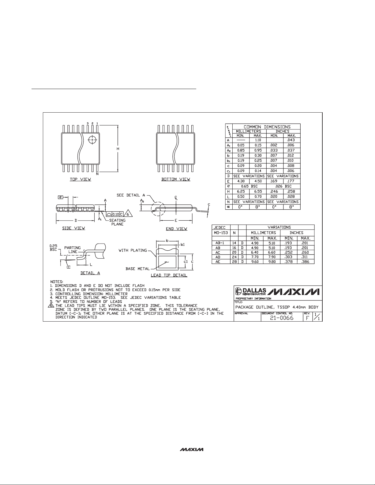
Package Information
(The package drawing(s) in this data sheet may not reflect the most current specifications. For the latest package outline information,
go to www.maxim-ic.com/packages.)
N
1
e
TOP VIEW
D
FRONT VIEW
INCHES
DIM
MIN
0.053A
0.004
A1
0.014
B
0.007
C
e 0.050 BSC 1.27 BSC
0.150
HE
A
B
A1
C
L
E
H 0.2440.228 5.80 6.20
0.016L
VARIATIONS:
INCHES
MINDIM
D
0.189 0.197 AA5.004.80 8
0.337 0.344 AB8.758.55 14
D
0-8
SIDE VIEW
MAX
0.069
0.010
0.019
0.010
0.157
0.050
MAX
0.3940.386D
MILLIMETERS
MAX
MIN
1.35
1.75
0.10
0.25
0.35
0.49
0.19
0.25
3.80 4.00
0.40 1.27
MILLIMETERS
MAX
MIN
9.80 10.00
N MS012
16
AC
SOICN .EPS
PROPRIETARY INFORMATION
TITLE:
PACKAGE OUTLINE, .150" SOIC
REV.DOCUMENT CONTROL NO.APPROVAL
21-0041
1
B
1
Page 14
MAX3030E–MAX3033E
±15kV ESD-Protected, 3.3V Quad
RS-422 Transmitters
Maxim cannot assume responsibility for use of any circuitry other than circuitry entirely embodied in a Maxim product. No circuit patent licenses are
implied. Maxim reserves the right to change the circuitry and specifications without notice at any time.
14 ____________________Maxim Integrated Products, 120 San Gabriel Drive, Sunnyvale, CA 94086 408-737-7600
© 2002 Maxim Integrated Products Printed USA is a registered trademark of Maxim Integrated Products.
Package Information (continued)
(The package drawing(s) in this data sheet may not reflect the most current specifications. For the latest package outline information,
go to www.maxim-ic.com/packages.)
TSSOP4.40mm.EPS
 Loading...