

Page 1
General Description
The MAX3013–MAX3022 8-channel level translators provide the level shifting necessary to allow 100Mbps data
transfer in a multivoltage system. Externally applied voltages, VCCand VL, set the logic levels on either side of
the device. Logic signals present on the VLside of the
device appear as a higher voltage logic signal on the
VCCside of the device, and vice-versa.
The MAX3013–MAX3022 feature an EN input that, when
at logic low, places all inputs/outputs on both sides in
tristate and reduces the VCCand VL supply currents to
0.1µA. These devices operate at a guaranteed data rate
of 100Mbps for V
L
> 1.8V.
The MAX3013–MAX3022 accept a V
CC
voltage from
+1.65V to +3.6V and a VLvoltage from +1.2V to (VCC-
0.4V), making them ideal for data transfer between lowvoltage ASICs/PLDs and higher voltage systems. The
MAX3013–MAX3022 are available in 5 x 4 UCSP™, 20pin 5mm x 5mm QFN, and 20-pin TSSOP packages.
Applications
Low-Voltage ASIC Level Translation
Cell Phones
SPI™, MICROWIRE™ Level Translation
Portable POS Systems
Portable Communication Devices
GPS
Telecommunications Equipment
Features
♦ 100Mbps Guaranteed Data Rate
♦ Bidirectional Level Translation (MAX3013)
♦ Unidirectional Level Translation
(MAX3014–MAX3022)
♦ V
L
Operation Down to +1.2V
♦ Ultra-Low 0.1µA Supply Current in Shutdown
♦ Low-Quiescent Current (0.1µA)
♦ UCSP, QFN, and TSSOP Packages
MAX3013–MAX3022
+1.2V to +3.6V, 0.1µA, 100Mbps,
8-Channel Level Translators
________________________________________________________________ Maxim Integrated Products 1
Ordering Information
19-3156; Rev 0; 1/04
For pricing, delivery, and ordering information, please contact Maxim/Dallas Direct! at
1-888-629-4642, or visit Maxim’s website at www.maxim-ic.com.
Ordering Information continued at end of data sheet.
Pin Configurations continued at end of data sheet.
Typical Operating Circuit appears at end of data sheet.
PART TEMP RANGE PIN-PACKAGE
N U M B ER O F
VL → V
C C
T R A N SL A T O R S
NUMBER OF
V
L
← V
CC
TRANSLATORS
DATA RATE
(Mbps)
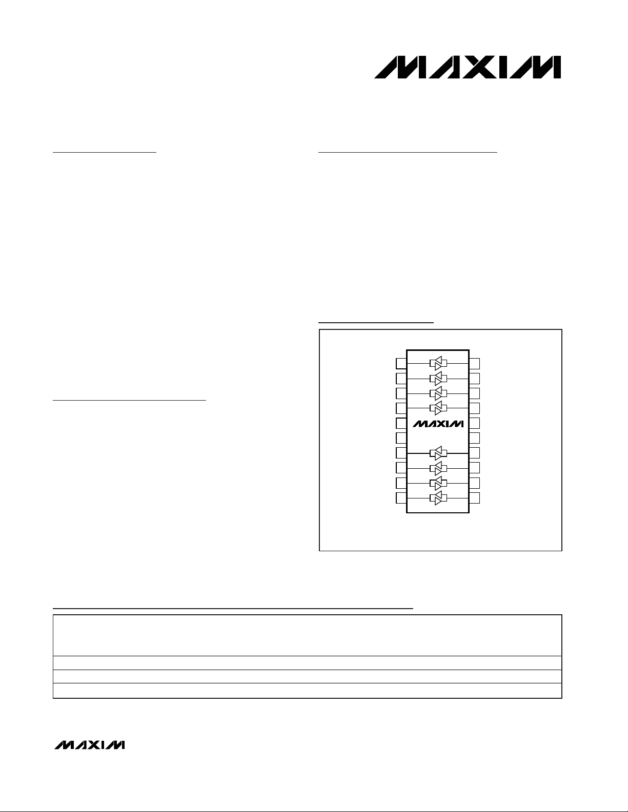
MAX3013EUP -40°C to +85°C 20 TSSOP 8 8 100
MAX3013EBP-T* -40°C to +85°C 5 x 4 UCSP 8 8 100
MAX3013EGP -40°C to +85°C 20 QFN-EP** 8 8 100
20
19
18
17
16
15
14
13
1
2
3
4
5
6
7
8
I/O V
CC
1
I/O V
CC
2
I/O V
CC
3
I/O V
CC
4I/O VL4
I/O V
L
3
I/O V
L
2
I/O V
L
1
V
CC
GND
I/O VCC5
I/O V
CC
6I/O VL6
I/O V
L
5
EN
V
L
12
11
9
10
I/O VCC7
I/O V
CC
8I/O VL8
I/O V
L
7
MAX3013
TSSOP
TOP VIEW
Pin Configurations
*Future Product—Contact factory for availability. **EP = Exposed paddle.
UCSP is a trademark of Maxim Integrated Products, Inc.
SPI is a trademark of Motorola, Inc.
MICROWIRE is a trademark of National Semiconductor Corp.
Page 2
MAX3013–MAX3022
+1.2V to +3.6V, 0.1µA, 100Mbps,
8-Channel Level Translators
2 _______________________________________________________________________________________
ABSOLUTE MAXIMUM RATINGS
ELECTRICAL CHARACTERISTICS
(VCC= +1.65V to +3.6V, VL= +1.2V to (VCC- 0.4V) (Note 1), EN = VL, C
IOVL
≤
15pF, C
IOVCC
≤
40pF, TA= T
MIN
to T
MAX
. Typical val-
ues are at V
CC
= +3.3V, VL= +1.8V, TA= +25°C.) (Note 2)
Stresses beyond those listed under “Absolute Maximum Ratings” may cause permanent damage to the device. These are stress ratings only, and functional
operation of the device at these or any other conditions beyond those indicated in the operational sections of the specifications is not implied. Exposure to
absolute maximum rating conditions for extended periods may affect device reliability.
(All voltages referenced to GND.)
VCC...........................................................................-0.3V to +4V
VL..............................................................................-0.3V to +4V
I/O VCC.......................................................-0.3V to (VCC+ 0.3V)
I/O VL.............................................................-0.3V to (VL+ 0.3V)
EN .................................................................-0.3V to (VL+ 0.3V)
Short-Circuit Duration I/O VL, I/O VCCto GND...........Continuous
Continuous Power Dissipation (TA= +70°C)
20-Pin TSSOP (derate 11mW/°C above +70°C) ..........879mW
5 x 4 UCSP (derate 10mW/°C above +70°C) ..............800mW
20-Pin QFN (derate 20.0mW/°C above +70°C) .............1.60W
Operating Temperature Range ...........................-40°C to +85°C
Junction Temperature......................................................+150°C
Storage Temperature Range .............................-65°C to +150°C
Lead Temperature (soldering, 10s) .................................+300°C
PARAMETER
SYMBOL
CONDITIONS
MIN
TYP
MAX
UNITS
POWER SUPPLIES
VL Supply Range V
L
1.2
V
CC
-
0.4
V
VCC Supply Range V
CC
3.6 V
Supply Current from V
CC
I
QVCC
I/O V
CC_
= 0, I/O V L _ = 0 or I/O V CC_ = VCC,
I/O V
L
_ = V
L
0.1 1 µA
I/O V CC_ = 0, I/O V L _ = 0 or I/O V CC_ = VCC,
I/O V
L
_ = V
L
0.1 4
Supply Current from V
L
I
QVL
I/O V CC_ = 0, I/O V L _ = 0 or I/O V CC_ = VCC,
I/O V
L
_ = VL, VL < VCC - 0.2V
0.1 100
µA
V
CC
Tristate Output Mode Supply
Current
TA = +25°C, EN = 0
1µA
TA = +25°C, EN = 0 0.1 0.2
V
L
Tristate Output Mode Supply
Current
I
TS-VL
TA = +25°C, EN = 0, VL = VCC - 0.2V 1 2
µA
TA = +25°C, EN = 0,
I/O Tristate Output Mode
Leakage Current
T
A
= +25°C, EN = 0, VL = VCC - 0.2V 30
µA
LOGIC-LEVEL THRESHOLDS
I/O VL_ Input-Voltage High V
IHL
2/3 x
V
L
V
I/O VL_ Input-Voltage Low V
ILL
1/3 x
V
L
V
I/O V
CC_
Input-Voltage High V
IHC
2/3 x
V
I/O V
CC_
Input-Voltage Low V
ILC
1/3 x
V
EN Input-Voltage High V
IH
TA = +25°C
2/3 x
V
L
V
1.65
I
TS-VCC
0.03
V
CC
0.15
V
CC
Page 3
MAX3013–MAX3022
+1.2V to +3.6V, 0.1µA, 100Mbps,
8-Channel Level Translators
_______________________________________________________________________________________ 3
ELECTRICAL CHARACTERISTICS (continued)
(VCC= +1.65V to +3.6V, VL= +1.2V to (VCC- 0.4V) (Note 1), EN = VL, C
IOVL
≤
15pF, C
IOVCC
≤
40pF, TA= T
MIN
to T
MAX
. Typical val-
ues are at V
CC
= +3.3V, VL= +1.8V, TA= +25°C.) (Note 2)
PARAMETER
CONDITIONS
UNITS
EN Input-Voltage Low V
IL
TA = +25°C
1/3 x
V
L
V
EN Input Current TA = +25°C±5µA
I/O VL_ Output-Voltage High V
OHL
I/O VL_ source current = 20µA
2/3 x
V
L
V
I/O VL_ Output-Voltage Low V
OLL
I/O VL_ sink current = 20µA
1/3 x
V
L
V
I/O V
CC_
Output-Voltage High V
OHC
I/O V
CC_
source current = 20µA
2/3 x
V
I/O V
CC_
Output-Voltage Low V
OLC
I/O V
CC_
sink current = 20µA
1/3 x
V
TIMING CHARACTERISTICS
(VCC= +1.65V to +3.6V, VL= +1.2V to (VCC- 0.4V) (Note 1), EN = VL, C
IOVL
≤
15pF, C
IOVCC
≤
40pF, TA= T
MIN
to T
MAX
. Typical val-
ues are at V
CC
= +3.3V, VL= +1.8V, TA= +25°C.) (Note 2)
PARAMETER
CONDITIONS
UNITS
C
IOV C C
= 15p F, Fi g ur e 1 2.5
C
IOV C C
= 20p F, Fi g ur e 1 3
I/O V
CC_
Rise Time t
RVCC
C
IOV C C
= 40p F, Fi g ur e 1 4
ns
C
IOV C C
= 15p F, Fi g ur e 1 2.5
C
IOV C C
= 20p F, Fi g ur e 1 3I/O V
CC_
Fall Time t
FVCC
C
IOV C C
= 40p F, Fi g ur e 1 4
ns
I/O V
CC_
One-Shot Output
Ω
I/O VL_ Rise Time t
RVL
C
IOVL
= 15pF, Figure 2 2.5 ns
I/O VL_ Fall Time t
FVL
C
IOVL
= 15pF, Figure 2 2.5 ns
I/O VL_ One-Shot Output
Impedance
Ω
Propagation Delay (Driving I/O
V
L_
)
C
IOV C C
= 15p F, Fi g ur e 1 6.5 ns
SYMBOL
SYMBOL
MIN TYP MAX
V
CC
MIN TYP MAX
V
CC
18.5
12.5
I/O
VL-VCC
Page 4
MAX3013–MAX3022
+1.2V to +3.6V, 0.1µA, 100Mbps,
8-Channel Level Translators
4 _______________________________________________________________________________________
Note 1: VLmust be less than or equal to VCC- 0.4V during normal operation. However, VLcan be greater than VCC- 0.4V during
starting up and shutting down conditions.
Note 2: All units are 100% production tested at T
A
= +25°C. Limits over the operating temperature range are guaranteed by design
and not production tested.
Note 3: Not production tested. Guaranteed by design.
TIMING CHARACTERISTICS (continued)
(VCC= +1.65V to +3.6V, VL= +1.2V to (VCC- 0.4V) (Note 1), EN = VL, C
IOVL
≤
15pF, C
IOVCC
≤
40pF, TA= T
MIN
to T
MAX
. Typical val-
ues are at V
CC
= +3.3V, VL= +1.8V, TA= +25°C.) (Note 2)
PARAMETER
SYMBOL
CONDITIONS
MIN
TYP
MAX
UNITS
Propagation Delay (Driving I/O
V
CC_
)
C
IOVL
= 15p F, Fi g ur e 2 6 ns
Part-to-Part Skew
C
IOV C C
= 15p F, C
IOVL
= 15p F, V
C C
= 2.5V ,
V
L
= 1.8V ( N ote 3)
4ns
Propagation Delay from I/O VL_ to
I/O V
CC_
after EN
C
IOV C C
= 15p F, Fi g ur e 3
ns
Propagation Delay from I/O V
CC_
to I/O VL_ after EN
t
EN-VL
C
IOVL
= 15p F, Fi g ur e 4
ns
C
IOV C C
= 15p F, C
IOVL
= 15p F, V L > 1.8V
Maximum Data Rate
C
IOV C C
= 15p F, C
IOVL
= 15p F, V L > 1.2V 80
Mbps
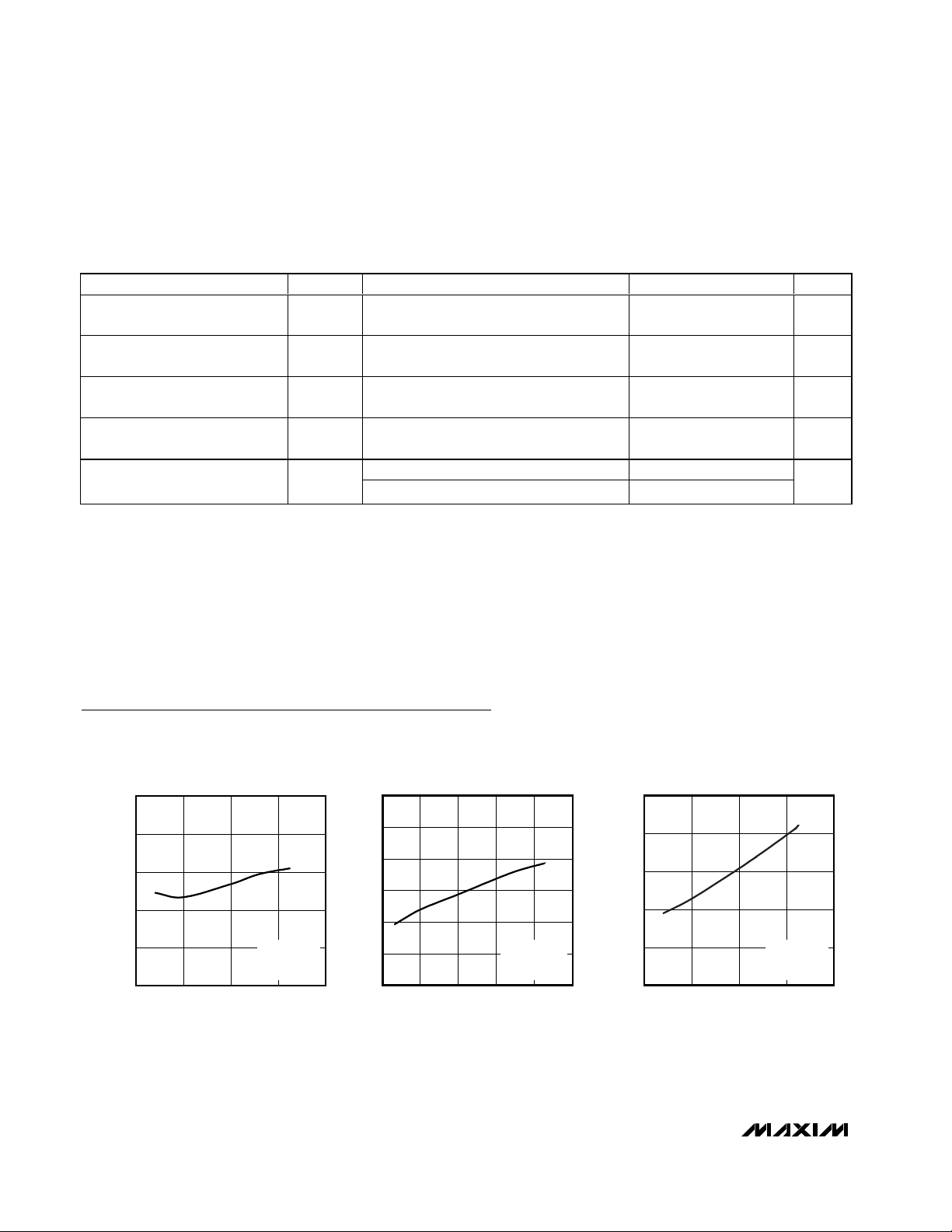
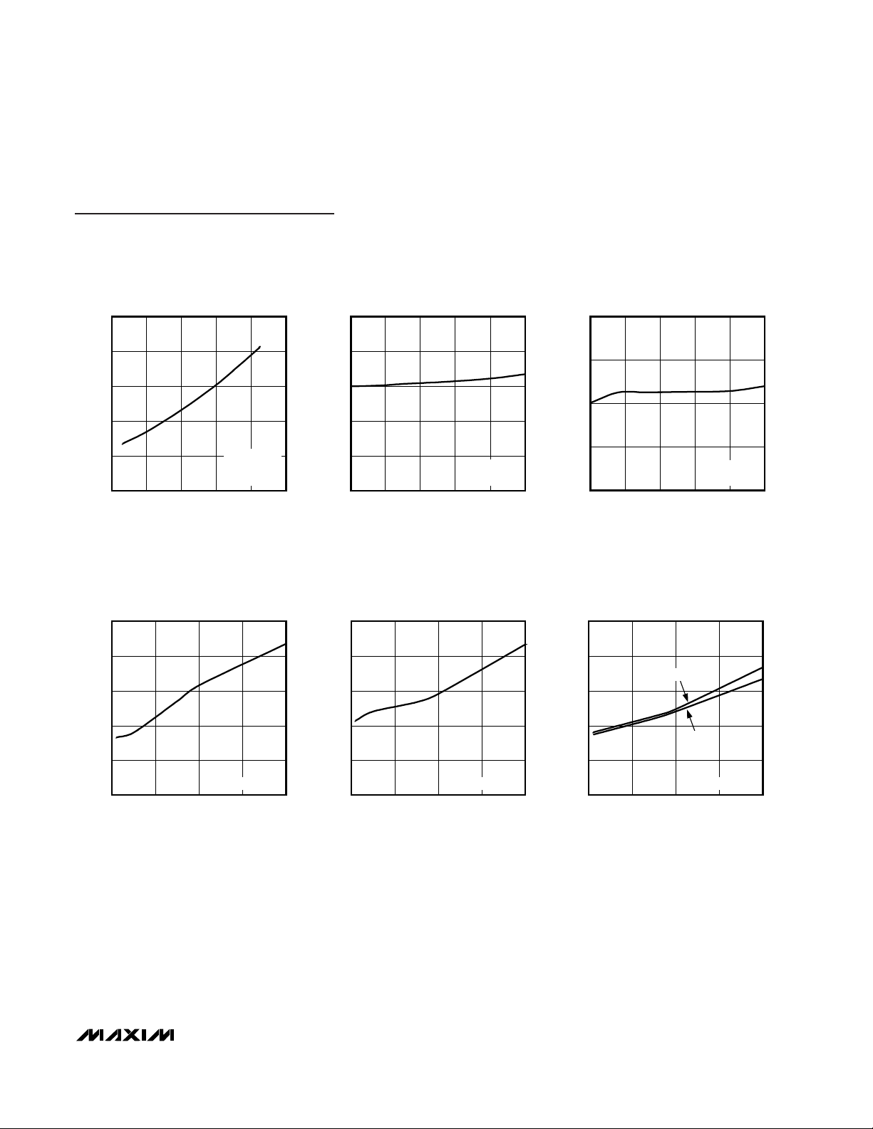
Typical Operating Characteristics
(Data rate = 100Mbps, VCC= 3.3V, VL= 1.8V, TA= +25°C, unless otherwise noted.)
0
0.2
0.1
0.4
0.3
0.5
0.6
VL SUPPLY CURRENT
vs. SUPPLY VOLTAGE
MAX3013 toc02
VCC SUPPLY VOLTAGE (V)
V
L
SUPPLY CURRENT (mA)
1.5 3.02.52.0 3.5 4.0
DRIVING I/O V
L
VL = 1.25V
C
IOVCC
= 15pF
0
0.2
0.6
0.4
0.8
1.0
VL SUPPLY CURRENT
vs. SUPPLY VOLTAGE
MAX3013 toc01
VCC SUPPLY VOLTAGE (V)
V
L
SUPPLY CURRENT (mA)
2.0 3.02.5 3.5 4.0
DRIVING I/O V
L
VL = 1.8V
C
IOVCC
= 15pF
0
5
15
10
20
25
VCC SUPPLY CURRENT
vs. SUPPLY VOLTAGE
MAX3013 toc03
VCC SUPPLY VOLTAGE (V)
V
CC
SUPPLY CURRENT (mA)
2.0 3.02.5 3.5 4.0
DRIVING I/O V
L
VL = 1.8V
C
IOVCC
= 15pF
I/O
VCC-VL
t
PPSKEW
t
EN-VCC
100
1000
1000
Page 5
MAX3013–MAX3022
+1.2V to +3.6V, 0.1µA, 100Mbps,
8-Channel Level Translators
_______________________________________________________________________________________ 5
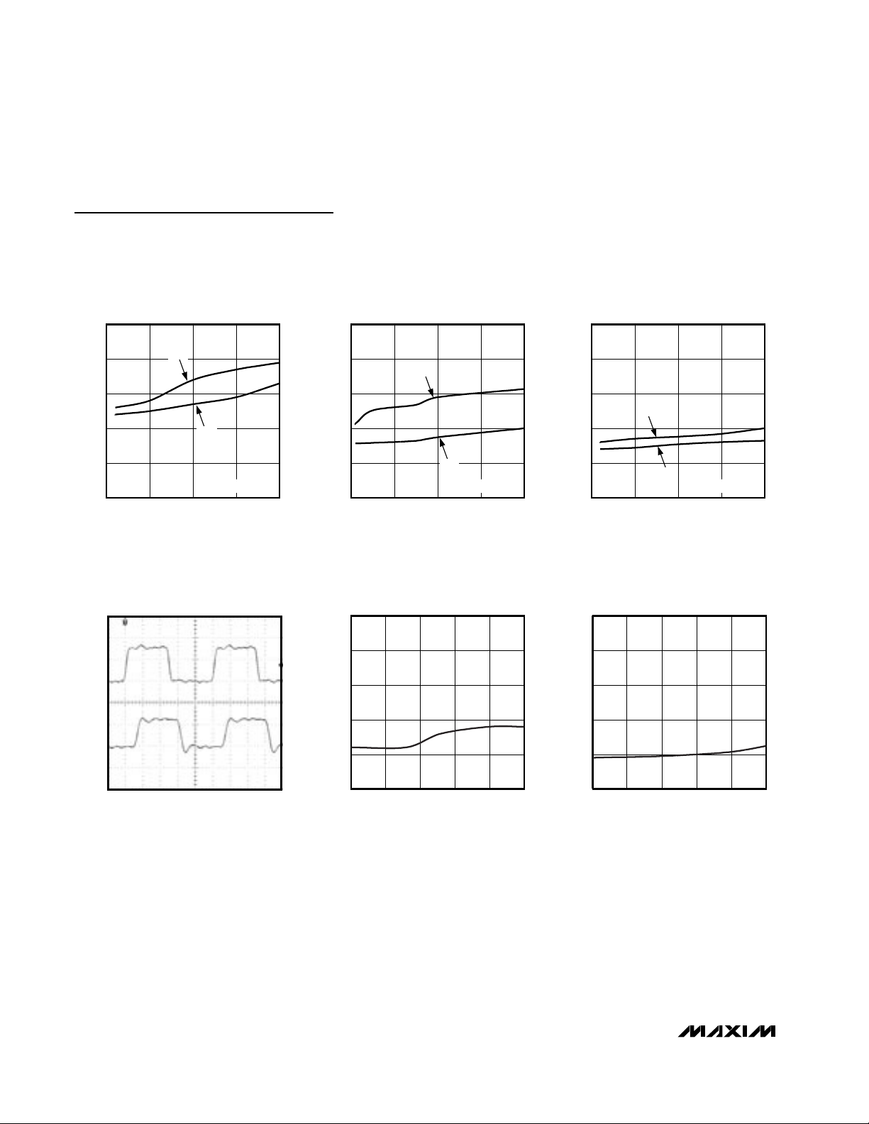
Typical Operating Characteristics (continued)
(Data rate = 100Mbps, VCC= 3.3V, VL= 1.8V, TA= +25°C, unless otherwise noted.)
0
5
15
10
20
25
VCC SUPPLY CURRENT
vs. SUPPLY VOLTAGE
MAX3013 toc04
VCC SUPPLY VOLTAGE (V)
V
CC
SUPPLY CURRENT (mA)
1.5 3.02.52.0 3.5 4.0
DRIVING I/O V
L
VL = 1.25V
C
IOVCC
= 15pF
2.0
2.4
3.2
2.8
3.6
4.0
VL SUPPLY CURRENT
vs. TEMPERATURE
MAX3013 toc05
TEMPERATURE (°C)
V
L
SUPPLY CURRENT (mA)
-40 3510-15 60 85
DRIVING I/O V
CC
C
IOVL
= 15pF
16
15
14
13
12
-40 10-15 35 60 85
VCC SUPPLY CURRENT
vs. TEMPERATURE
MAX3013 toc06
TEMPERATURE (°C)
V
CC
SUPPLY CURRENT (mA)
DRIVING I/O V
CC
C
IOVL
= 15pF
0
0.2
0.6
0.4
0.8
1.0
VL SUPPLY CURRENT
vs. CAPACITIVE LOAD ON I/O V
CC
MAX3013toc07
CAPACITIVE LOAD (pF)
V
L
SUPPLY CURRENT (mA)
02010 30 40
DRIVING I/O V
L
10
13
19
16
22
25
VCC SUPPLY CURRENT
vs. CAPACITIVE LOAD ON I/O V
CC
MAX3013 toc08
CAPACITIVE LOAD (pF)
V
CC
SUPPLY CURRENT (mA)
02010 30 40
DRIVING I/O V
L
0
0.3
0.9
0.6
1.2
1.5
RISE/FALL TIME
vs. CAPACITIVE LOAD ON I/O V
CC
MAX3013 toc09
CAPACITIVE LOAD (pF)
RISE/FALL TIME (ns)
02010 30 40
DRIVING I/O V
L
t
FALL
t
RISE
Page 6
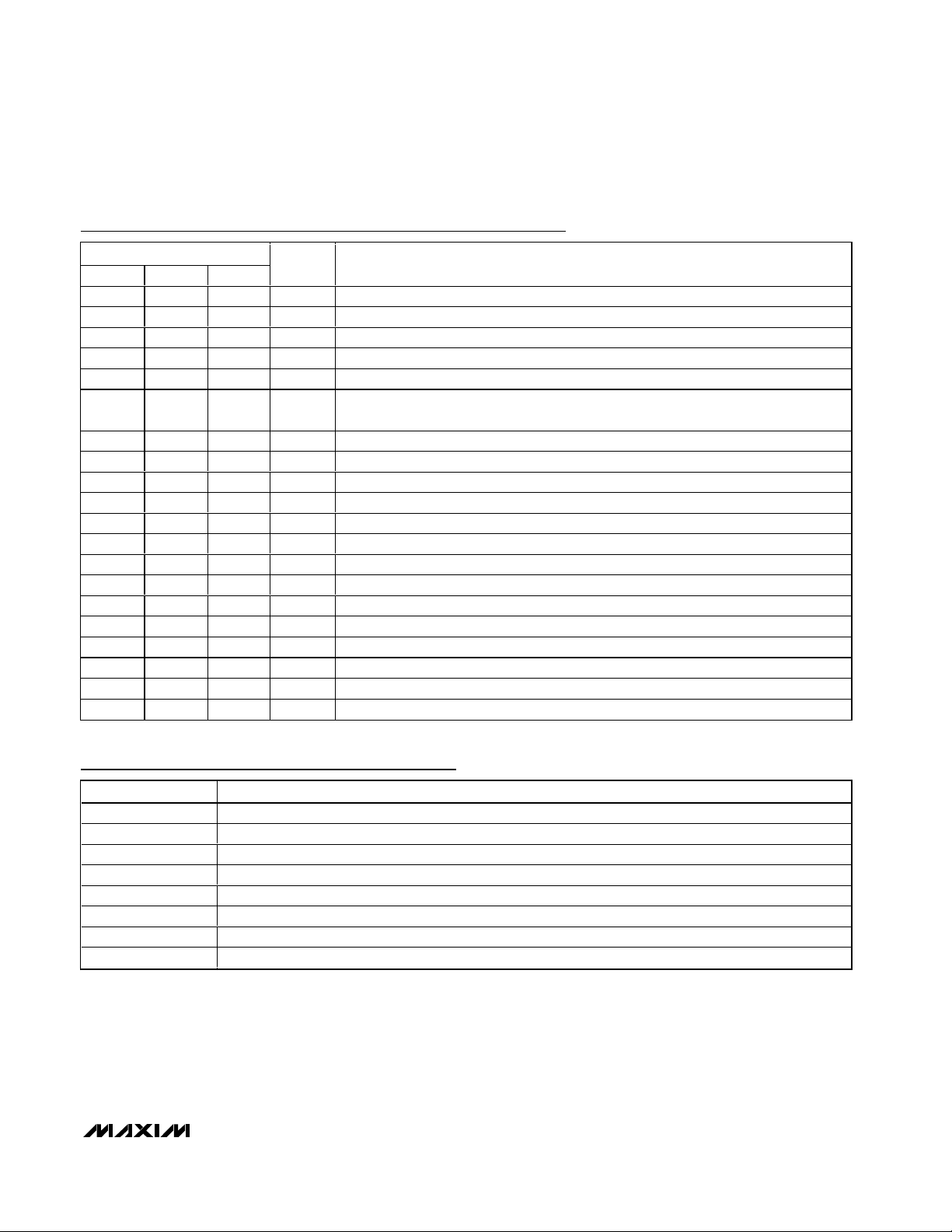
Typical Operating Characteristics (continued)
(Data rate = 100Mbps, VCC= 3.3V, VL= 1.8V, TA= +25°C, unless otherwise noted.)
MAX3013–MAX3022
+1.2V to +3.6V, 0.1µA, 100Mbps,
8-Channel Level Translators
6 _______________________________________________________________________________________
0
0.2
0.6
0.4
0.8
1.0
RISE/FALL TIME
vs. CAPACITIVE LOAD ON I/O V
L
MAX3013 toc10
CAPACITIVE LOAD (pF)
RISE/FALL TIME (ns)
01051520
DRIVING I/O V
CC
t
FALL
t
RISE
0
1
3
2
4
5
PROPAGATION DELAY
vs. CAPACITIVE LOAD ON I/O V
CC
MAX3013 toc11
CAPACITIVE LOAD (pF)
PROPAGATION DELAY (ns)
02010 30 40
DRIVING I/O V
L
t
PHL
t
PLH
0
1
3
2
4
5
PROPAGATION DELAY
vs. CAPACITIVE LOAD ON I/O V
L
MAX3013 toc12
CAPACITIVE LOAD (pF)
PROPAGATION DELAY (ns)
01051520
DRIVING I/O V
CC
t
PHL
t
PLH
TYPICAL I/O VCC DRIVING
MAX3013 toc13
I/O V
CC
1V/div
I/O V
L
1V/div
4ns/div
150
160
180
170
190
200
t
EN-VCC
vs. TEMPERATURE
(C
IOVCC
= 15pF)
MAX3013 toc14
TEMPERATURE (°C)
t
EN-VCC
(ns)
-40 3510-15 60 85
0
20
60
40
80
100
t
EN-VL
vs. TEMPERATURE
(C
IOVL
= 15pF)
MAX3013 toc15
TEMPERATURE (°C)
t
EN-VL
(ns)
-40 3510-15 60 85
Page 7
MAX3013–MAX3022
+1.2V to +3.6V, 0.1µA, 100Mbps,
8-Channel Level Translators
_______________________________________________________________________________________ 7
Pin Description (MAX3013)
PIN
TSSOP
QFN
FUNCTION
1 18 B1
Input/Output 1, Referenced to V
L
2 19 A1
Input/Output 2, Referenced to V
L
3 20 B2
Input/Output 3, Referenced to V
L
4 1 A2
Input/Output 4, Referenced to V
L
5 2 A3 V
L
VL Input Voltage, +1.2V ≤ VL ≤ (VCC - 0.4V). Bypass VL to GND with a 0.1µF capacitor.
6 3 A4 EN
Enable Input. If EN is pulled low, all inputs/outputs are in tristate. Drive EN high (VL) for
normal operation.
7 4 B3
Input/Output 5, Referenced to V
L
8 5 A5
Input/Output 6, Referenced to V
L
9 6 B4
Input/Output 7, Referenced to V
L
10 7 B5
Input/Output 7, Referenced to V
L
11 8 C5
Input/Output 8, Referenced to V
CC
12 9 C4
Input/Output 7, Referenced to V
CC
13 10 D5
Input/Output 6, Referenced to V
CC
14 11 C3
Input/Output 5, Referenced to V
CC
15 12 D4
Ground
16 13 D3 V
CC
VCC Input Voltage, +1.65V ≤ V
CC
≤ +3.6V. Bypass VCC to GND with a 0.1µF capacitor.
17 14 D2
Input/Output 4, Referenced to V
CC
18 15 C2
Input/Output 3, Referenced to V
CC
19 16 D1
Input/Output 2, Referenced to V
CC
20 17 C1
Input/Output 1, Referenced to V
CC
Pin Description (MAX3014–MAX3022)
NAME FUNCTION (Note 4)
V
CC
V
CC
Input Voltage, +1.65V ≤ VCC ≤ +3.6V. Bypass VCC to GND with a 0.1µF capacitor.
V
L
VL Input Voltage, +1.2V ≤ VL ≤ VCC - 0.4V. Bypass VL to GND with a 0.1µF capacitor.
GND Ground
EN Enable Input. If EN is pulled low, all inputs/outputs are in tristate. Drive EN high (VL) for normal operation.
IVL1–IVL8Inputs Referenced to VL, Numbers 1 to 8
OVL1–OVL8 Outputs Referenced to VL, Numbers 1 to 8
IVCC1–IVCC8Inputs Referenced to VCC, Numbers 1 to 8
OVCC1–OVCC8 Outputs Referenced to VCC, Numbers 1 to 8
Note 4: For specific pin numbers, see the Pin Configurations for more information.
UCSP
NAME
I/O VL1
I/O VL2
I/O VL3
I/O VL4
I/O VL5
I/O VL6
I/O VL7
I/O VL8
I/O VCC8
I/O VCC7
I/O VCC6
I/O VCC5
GND
I/O VCC4
I/O VCC3
I/O VCC2
I/O VCC1
Page 8

MAX3013–MAX3022
+1.2V to +3.6V, 0.1µA, 100Mbps,
8-Channel Level Translators
8 _______________________________________________________________________________________
MAX3013
I/O V
CC
I/O V
CC
C
IOVCC
V
CC
V
L
I/O V
L
SOURCE
90%
50%
10%
t
FVCC
t
RVCC
I/O V
L
90%
50%
10%
EN
I/O
VL-VCC
I/O
VL-VCC
t
RISE/FALL
≤ 3ns
Test Circuits/Timing Diagrams
Figure 1. Driving I/O VLTest Circuit and Timing
Page 9

MAX3013–MAX3022
+1.2V to +3.6V, 0.1µA, 100Mbps,
8-Channel Level Translators
_______________________________________________________________________________________ 9
MAX3013
I/O V
L
I/O V
CC
V
CC
V
L
I/O V
L
C
IOVL
SOURCE
90%
50%
10%
t
FVL
t
RVL
I/O V
CC
90%
50%
10%
EN
I/O
VCC-VL
I/O
VCC-VL
t
RISE/FALL
≤ 3ns
Figure 2. Driving I/O VCCTest Circuit and Timing
Test Circuits/Timing Diagrams (continued)
Page 10

MAX3013–MAX3022
+1.2V to +3.6V, 0.1µA, 100Mbps,
8-Channel Level Translators
10 ______________________________________________________________________________________
MAX3013
I/O V
CC
V
L
C
IOVCC
I/O V
L
SOURCE
EN
t'
EN-VCC
MAX3013
I/O V
CC
I/O V
L
V
L
V
L
0V
I/O V
CC
VCC/2
V
CC
0V
0V
EN
C
IOVCC
I/O V
L
SOURCE
EN
t"
EN-VCC
I/O V
L
V
L
V
L
0V
I/O V
CC
VCC/2
V
CC
0V
0V
EN
t
EN-VCC
IS WHICHEVER IS LARGER BETWEEN t'
EN-VCC
AND t"
EN-VCC
.
Figure 3. Propagation Delay from I/O VLto I/O VCCafter EN
MAX3013
I/O V
CC
C
IOVL
V
CC
I/O V
L
SOURCE
EN
t'
EN-VL
MAX3013
I/O V
CC
I/O V
CC
V
L
V
CC
0V
I/O V
L
VL/2
V
L
0V
0V
EN
C
IOVL
I/O V
L
SOURCE
EN
t"
EN-VL
I/O V
CC
V
L
V
CC
0V
I/O V
L
VL/2
V
L
0V
0V
EN
t
EN-VCC
IS WHICHEVER IS LARGER BETWEEN t'
EN-VCC
AND t"
EN-VCC
.
Figure 4. Propagation Delay from I/O VCCto I/O VLafter EN
Test Circuits/Timing Diagrams (continued)
Page 11

MAX3013–MAX3022
+1.2V to +3.6V, 0.1µA, 100Mbps,
8-Channel Level Translators
______________________________________________________________________________________ 11
Detailed Description
The MAX3013–MAX3022 logic-level translators provide
the level shifting necessary to allow 100Mbps data transfer in a multivoltage system. Externally applied voltages,
VCCand VL, set the logic levels on either side of the
device. Logic signals present on the VLside of the
device appear as a higher voltage logic signal on the
VCCside of the device, and vice-versa. The MAX3013
bidirectional level translator allows data translation in
either direction (VL↔ VCC) on any single data line. The
MAX3014–MAX3022 unidirectional translators level-shift
data in one direction (V
L
→ VCCor VCC→ VL) on any
single data line. The MAX3013–MAX3022 accept V
L
from
+1.2V to (VCC- 0.4V) and operate with VCCfrom +1.65V
to +3.6V, making them ideal for data transfer between
low-voltage ASICs/PLDs and higher voltage systems.
The MAX3013–MAX3022 feature an input enable mode
(EN) that reduces VCCand VLsupply currents to 0.1µA,
when in tristate mode. These devices operate at a
guaranteed data rate of 100Mbps for VL> +1.8V.
Level Translation
For proper operation, ensure that +1.65V ≤ VCC≤ +3.6V,
+1.2V ≤ VL≤ (VCC- 0.4V). During power-up sequencing,
VL≥ VCCdoes not damage the device. During powersupply sequencing, when VCCis floating and VLis powering up, up to 40mA current can be sourced to each
load on the VLside, yet the device does not latch up.
The maximum data rate depends heavily on the load
capacitance (see the Typical Operating Characteristics,
Rise/Fall Times), output impedance of the driver, and the
operating voltage range (see the Timing Characteristics).
Input Driver Requirements
The MAX3013–MAX3022 architecture is based on a
one-shot accelerator output stage (see Figure 5).
Accelerator output stages are always in tristate mode
except when there is a transition on any of the translators on the input side, either I/O VLor I/O VCC. Then, a
short pulse is generated during which the accelerator
output stages become active and charge/discharge the
capacitances at the I/Os. Due to its bidirectional nature,
both input stages become active during the one-shot
pulse. This can lead to some current feeding into the
external source that is driving the translator. However,
this behavior helps to speed up the transition on the
driven side.
For proper operation, the external driver must meet the
following conditions: <25Ω output impedance and
>20mA output current. Figure 6 shows a graph of
Typical Input Current vs. Input Voltage.
Output Load Requirements
The MAX3013–MAX3022 I/O were designed to drive
CMOS inputs. Do not load the I/O lines with a resistive
load less than 25kΩ. Also, do not place an RC circuit at
the input of the MAX3013–MAX3022 to slow down the
edges. If a slower data rate is required, please see the
MAX3000E/MAX3001E logic-level translator.
For I2C™ level translation, please refer to the MAX3372E–
MAX3379E/MAX3390E–MAX3393E data sheet.
OV
CC
V
L
IV
L
V
CC
P
ONE-SHOT
N
ONE-SHOT
TYPICAL DRIVING ONE-CHANNEL ON V
L
SIDE
150
Ω
4k
Ω
IV
CC
V
L
OV
L
V
CC
TYPICAL DRIVING ONE-CHANNEL ON VCC SIDE
4k
Ω
150
Ω
N
ONE-SHOT
P
ONE-SHOT
Figure 5. MAX3013–MAX3022 Simplified Diagram (1 I/O line)
I2C is a trademark of Philips Corp. Purchase of I2C components
of Maxim Integrated Products, Inc. or one of its sublicensed
Associated Companies, conveys a license under the Philips I
2
C
Patent Rights to use these components in an I
2
C system, provid-
ed that the system conforms to the I
2
C Standard Specification
as defined by Philips.
Page 12

MAX3013–MAX3022
+1.2V to +3.6V, 0.1µA, 100Mbps,
8-Channel Level Translators
12 ______________________________________________________________________________________
Enable Input (EN)
The MAX3013–MAX3022 feature an EN input. Pull EN
low to set the MAX3013–MAX3022’s I/O on both sides
in tristate output mode. Drive EN to logic high (VL) for
normal operation.
Applications Information
Power-Supply Decoupling
To reduce ripple and the chance of introducing data
errors, bypass VLand VCCto ground with a 0.1µF
ceramic capacitor. Place the bypass capacitors as
close to the power-supply input pins as possible.
8-Bit Bus Translation
The MAX3013–MAX3022 level-shift the data present on
the I/O line between +1.2V to +3.6V, making them ideal
for level translation between a low-voltage ASIC and a
higher voltage system. The Typical Operating Circuit
shows the MAX3013 bidirectional translator in an 8-bit
bus level translation from a 1.8V system to a 3.3V system and vice versa.
Unidirectional vs. Bidirectional Level
Translator
The MAX3013 bidirectional translator can operate as a
unidirectional device to translate signals without inversion. The MAX3014–MAX3022 unidirectional translators
level-shift data in one direction (VL→ VCCor VCC→ VL)
on any single data line (see the Ordering Information).
These devices provide the smallest solution (UCSP package) for unidirectional level translation without inversion.
0V
V
TH_IN/RIN
*
-(V
S
- V
TH_IN
)/RIN*
I
IN
V
TH_IN
*RIN = 4kΩ WHEN DRIVING VL SIDE.
R
IN
= 150Ω WHEN DRIVING VCC SIDE.
V
S
V
IN
WHERE VS = VCC OR VL.
Figure 6. Typical IINvs. V
IN
MAX3013
+1.8V
+3.3V
+1.8V
SYSTEM
CONTROLLER
+3.3V
SYSTEM
GND
V
L
V
CC
EN
BIT 1
BIT 2
BIT 0
BIT 3
BIT 4
BIT 5
BIT 6
BIT 7
BIT 1
BIT 2
BIT 0
BIT 3
BIT 4
BIT 5
BIT 6
BIT 7
I/O V
CC
1
I/O V
CC
2
I/O V
CC
3
I/O V
CC
4I/O VL4
I/O V
L
3
I/O V
L
2
I/O V
L
1
0.1µF0.1µF
I/O VCC5
I/O V
CC
6I/O VL6
I/O V
L
5
I/O VCC7
I/O V
CC
8I/O VL8
I/O V
L
7
Typical Operating Circuit
Chip Information
TRANSISTOR COUNT: 1447
PROCESS: BiCMOS
Page 13

MAX3013–MAX3022
+1.2V to +3.6V, 0.1µA, 100Mbps,
8-Channel Level Translators
______________________________________________________________________________________ 13
Ordering Information (continued)
PART TEMP RANGE PIN-PACKAGE
N U M B ER O F
V
L
→ V
C C
T R A N SL A T O R S
NUMBER OF
V
L
← V
CC
TRANSLATORS
DATA RATE
(Mbps)
MAX3014EUP* -40°C to +85°C 20 TSSOP 8 0 100
MAX3014EBP-T* -40°C to +85°C 5 x 4 UCSP 8 0 100
MAX3014EGP* -40°C to +85°C 20 QFN-EP** 8 0 100
MAX3015EUP* -40°C to +85°C 20 TSSOP 7 1 100
MAX3015EBP-T* -40°C to +85°C 5 x 4 UCSP 7 1 100
MAX3015EGP* -40°C to +85°C 20 QFN-EP** 7 1 100
MAX3016EUP* -40°C to +85°C 20 TSSOP 6 2 100
MAX3016EBP-T* -40°C to +85°C 5 x 4 UCSP 6 2 100
MAX3016EGP* -40°C to +85°C 20 QFN-EP** 6 2 100
MAX3017EUP* -40°C to +85°C 20 TSSOP 5 3 100
MAX3017EBP-T* -40°C to +85°C 5 x 4 UCSP 5 3 100
MAX3017EGP* -40°C to +85°C 20 QFN-EP** 5 3 100
MAX3018EUP* -40°C to +85°C 20 TSSOP 4 4 100
MAX3018EBP-T* -40°C to +85°C 5 x 4 UCSP 4 4 100
MAX3018EGP* -40°C to +85°C 20 QFN-EP** 4 4 100
MAX3019EUP* -40°C to +85°C 20 TSSOP 3 5 100
MAX3019EBP-T* -40°C to +85°C 5 x 4 UCSP 3 5 100
MAX3019EGP* -40°C to +85°C 20 QFN-EP** 3 5 100
MAX3020EUP* -40°C to +85°C 20 TSSOP 2 6 100
MAX3020EBP-T* -40°C to +85°C 5 x 4 UCSP 2 6 100
MAX3020EGP* -40°C to +85°C 20 QFN-EP** 2 6 100
MAX3021EUP* -40°C to +85°C 20 TSSOP 1 7 100
MAX3021EBP-T* -40°C to +85°C 5 x 4 UCSP 1 7 100
MAX3021EGP* -40°C to +85°C 20 QFN-EP** 1 7 100
MAX3022EUP* -40°C to +85°C 20 TSSOP 0 8 100
MAX3022EBP-T* -40°C to +85°C 5 x 4 UCSP 0 8 100
MAX3022EGP* -40°C to +85°C 20 QFN-EP** 0 8 100
*Future Product—Contact factory for availability.
**EP = Exposed paddle.
Page 14

MAX3013–MAX3022
+1.2V to +3.6V, 0.1µA, 100Mbps,
8-Channel Level Translators
14 ______________________________________________________________________________________
20
19
18
17
16
15
14
13
1
2
3
4
5
6
7
8
OV
CC
1
OV
CC
2
OV
CC
3
OV
CC
4IVL4
IV
L
3
IV
L
2
IV
L
1
V
CC
GND
OVCC5
OV
CC
6IVL6
IV
L
5
EN
V
L
12
11
9
10
OVCC7
OV
CC
8IVL8
IV
L
7
MAX3014
TSSOP
20
19
18
17
16
15
14
13
1
2
3
4
5
6
7
8
IV
CC
1
OV
CC
2
OV
CC
3
OV
CC
4IVL4
IV
L
3
IV
L
2
OV
L
1
V
CC
GND
OVCC5
OV
CC
6IVL6
IV
L
5
EN
V
L
12
11
9
10
OVCC7
OV
CC
8IVL8
IV
L
7
MAX3015
TSSOP
20
19
18
17
16
15
14
13
1
2
3
4
5
6
7
8
IV
CC
1
IV
CC
2
OV
CC
3
OV
CC
4IVL4
IV
L
3
OV
L
2
OV
L
1
V
CC
GND
OVCC5
OV
CC
6IVL6
IV
L
5
EN
V
L
12
11
9
10
OVCC7
OV
CC
8IVL8
IV
L
7
MAX3016
TSSOP
20
19
18
17
16
15
14
13
1
2
3
4
5
6
7
8
IVCC1
IV
CC
2
IV
CC
3
OV
CC
4IVL4
OV
L
3
OV
L
2
OV
L
1
V
CC
GND
OVCC5
OV
CC
6IVL6
IV
L
5
EN
V
L
12
11
9
10
OVCC7
OV
CC
8IVL8
IV
L
7
MAX3017
TSSOP
20
19
18
17
16
15
14
13
1
2
3
4
5
6
7
8
IVCC1
IV
CC
2
IV
CC
3
IV
CC
4OVL4
OV
L
3
OV
L
2
OV
L
1
V
CC
GND
IVCC5
OV
CC
6IVL6
OV
L
5
EN
V
L
12
11
9
10
OVCC7
OV
CC
8IVL8
IV
L
7
MAX3019
TSSOP
20
19
18
17
16
15
14
13
1
2
3
4
5
6
7
8
IVCC1
IV
CC
2
IV
CC
3
IV
CC
4OVL4
OV
L
3
OV
L
2
OV
L
1
V
CC
GND
IVCC5
IV
CC
6OVL6
OV
L
5
EN
V
L
12
11
9
10
OVCC7
OV
CC
8IVL8
IV
L
7
MAX3020
TSSOP
20
19
18
17
16
15
14
13
1
2
3
4
5
6
7
8
IVCC1
IV
CC
2
IV
CC
3
IV
CC
4OVL4
OV
L
3
OV
L
2
OV
L
1
V
CC
GND
IVCC5
IV
CC
6OVL6
OV
L
5
EN
V
L
12
11
9
10
IVCC7
OV
CC
8IVL8
OV
L
7
MAX3021
TSSOP
20
19
18
17
16
15
14
13
1
2
3
4
5
6
7
8
IVCC1
IV
CC
2
IV
CC
3
IV
CC
4OVL4
OV
L
3
OV
L
2
OV
L
1
V
CC
GND
IVCC5
IV
CC
6OVL6
OV
L
5
EN
V
L
12
11
9
10
IVCC7
IV
CC
8OVL8
OV
L
7
MAX3022
TSSOP
20
19
18
17
16
15
14
13
1
2
3
4
5
6
7
8
IVCC1
IV
CC
2
IV
CC
3
IV
CC
4OVL4
OV
L
3
OV
L
2
OV
L
1
V
CC
GND
OVCC5
OV
CC
6IVL6
IV
L
5
EN
V
L
12
11
9
10
OVCC7
OV
CC
8IVL8
IV
L
7
MAX3018
TSSOP
Pin Configurations (continued)
Page 15

MAX3013–MAX3022
+1.2V to +3.6V, 0.1µA, 100Mbps,
8-Channel Level Translators
______________________________________________________________________________________ 15
MAX3013
20 UCSP
(BOTTOM VIEW)
MAX3014
20 UCSP
(BOTTOM VIEW)
I/O VCC4I/O VCC2 V
CC
GND
I/O V
CC
3I/O VCC1 I/O VCC5 I/O VCC7
I/O VL3I/O VL1 I/O VL5 I/O VL7
I/O VL4I/O VL2V
L
EN
I/O VCC6
I/O V
CC
8
I/O VL8
I/O VL6
1
B
A
C
D
2345
V
CC
OVCC2 GND OVCC6
OV
CC
5OVCC1OV
CC
7OVCC8
IV
L
5IVL1IV
L
7IVL8
V
L
IVL2ENIV
L
6
OVCC4
OV
CC
3
IV
L
3
IVL4
1
B
A
C
D
3452
MAX3015
20 UCSP
(BOTTOM VIEW)
V
CC
OVCC2 GND OVCC6
OV
CC
5OVCC1OV
CC
7OVCC8
IV
L
5OVL1IV
L
7IVL8
V
L
IVL2ENIV
L
6
OVCC4
OV
CC
3
IV
L
3
IVL4
1
B
A
C
D
3452
MAX3016
20 UCSP
(BOTTOM VIEW)
V
CC
IVCC2 GND OVCC6
OV
CC
5IVCC1OV
CC
7OVCC8
IV
L
5OVL1IV
L
7IVL8
V
L
OVL2ENIV
L
6
OVCC4
OV
CC
3
IV
L
3
IVL4
1
B
A
C
D
3452
MAX3017
20 UCSP
(BOTTOM VIEW)
V
CC
IVCC2 GND OVCC6
OV
CC
5IVCC1OV
CC
7OVCC8
IVL5OVL1IV
L
7IVL8
V
L
OVL2ENIV
L
6
OVCC4
IV
CC
3
OVL3
IVL4
1
B
A
C
D
3452
MAX3018
20 UCSP
(BOTTOM VIEW)
V
CC
IVCC2 GND OVCC6
OV
CC
5IVCC1OV
CC
7OVCC8
IVL5OVL1IV
L
7IVL8
V
L
OVL2ENIV
L
6
IVCC4
IV
CC
3
OVL3
OVL4
1
B
A
C
D
3452
Pin Configurations (continued)
Page 16

MAX3013–MAX3022
+1.2V to +3.6V, 0.1µA, 100Mbps,
8-Channel Level Translators
16 ______________________________________________________________________________________
MAX3019
20 UCSP
(BOTTOM VIEW)
V
CC
IVCC2 GND OVCC6
IV
CC
5IVCC1OV
CC
7OVCC8
OVL5OVL1IV
L
7IVL8
V
L
OVL2ENIV
L
6
IVCC4
IV
CC
3
OVL3
OVL4
1
B
A
C
D
3452
MAX3020
20 UCSP
(BOTTOM VIEW)
V
CC
IVCC2 GND IVCC6
IV
CC
5IVCC1OV
CC
7OVCC8
OVL5OVL1IV
L
7IVL8
V
L
OVL2ENOV
L
6
IVCC4
IV
CC
3
OVL3
OVL4
1
B
A
C
D
3452
MAX3021
20 UCSP
(BOTTOM VIEW)
V
CC
IVCC2 GND IVCC6
IV
CC
5IVCC1IV
CC
7OVCC8
OVL5OVL1OV
L
7IVL8
V
L
OVL2ENOV
L
6
IVCC4
IV
CC
3
OVL3
OVL4
1
B
A
C
D
3452
MAX3022
20 UCSP
(BOTTOM VIEW)
V
CC
IVCC2 GND IVCC6
IV
CC
5IVCC1IV
CC
7IVCC8
OVL5OVL1OV
L
7OVL8
V
L
OVL2ENOV
L
6
IVCC4
IV
CC
3
OVL3
OVL4
1
B
A
C
D
3452
Pin Configurations (continued)
Page 17

MAX3013–MAX3022
+1.2V to +3.6V, 0.1µA, 100Mbps,
8-Channel Level Translators
______________________________________________________________________________________ 17
20
19
18
17
16
I/O V
L
3
I/O V
L
2
I/O V
L
1
I/O V
CC
1
I/O V
CC
2
6
7
8
9
10
I/O V
L
7
I/O V
L
8
I/O V
CC
8
I/O V
CC
7
I/O V
CC
6
11
12
13
14
15
I/O V
CC
5
GND
V
CC
I/O V
CC
4
I/O V
CC
3
5
4
3
2
1
I/O V
L
6
I/O V
L
5
EN
**EXPOSED PADDLE
V
L
I/O VL4
MAX3013
5mm x 5mm QFN
TOP VIEW
20
19
18
17
16
IV
L
3
IV
L
2
IV
L
1
OV
CC
1
OV
CC
2
6
7
8
9
10
IV
L
7
IV
L
8
OV
CC
8
OV
CC
7
OV
CC
6
11
12
13
14
15
OV
CC
5
GND
V
CC
OV
CC
4
OV
CC
3
5
4
3
2
1
IV
L
6
IV
L
5
EN
**EXPOSED PADDLE
V
L
IVL4
MAX3014
5mm x 5mm QFN
20
19
18
17
16
IV
L
3
IV
L
2
OV
L
1
IV
CC
1
OV
CC
2
6
7
8
9
10
IV
L
7
IV
L
8
OV
CC
8
OV
CC
7
OV
CC
6
11
12
13
14
15
OVCC5
GND
V
CC
OV
CC
4
OV
CC
3
5
4
3
2
1
IV
L
6
IV
L
5
EN
**EXPOSED PADDLE
V
L
IVL4
MAX3015
5mm x 5mm QFN
20
19
18
17
16
IV
L
3
OV
L
2
OV
L
1
IV
CC
1
IV
CC
2
6
7
8
9
10
IV
L
7
IV
L
8
OV
CC
8
OV
CC
7
OV
CC
6
11
12
13
14
15
OVCC5
GND
V
CC
OV
CC
4
OV
CC
3
5
4
3
2
1
IV
L
6
IV
L
5
EN
**EXPOSED PADDLE
V
L
IVL4
MAX3016
5mm x 5mm QFN
20
19
18
17
16
OV
L
3
OV
L
2
OV
L
1
IV
CC
1
IV
CC
2
6
7
8
9
10
IV
L
7
IV
L
8
OV
CC
8
OV
CC
7
OV
CC
6
11
12
13
14
15
OVCC5
GND
V
CC
OV
CC
4
IV
CC
3
5
4
3
2
1
IV
L
6
IV
L
5
EN
**EXPOSED PADDLE
V
L
IVL4
MAX3017
5mm x 5mm QFN
20
19
18
17
16
OV
L
3
OV
L
2
OV
L
1
IV
CC
1
IV
CC
2
6
7
8
9
10
IV
L
7
IV
L
8
OV
CC
8
OV
CC
7
OV
CC
6
11
12
13
14
15
OVCC5
GND
V
CC
IV
CC
4
IV
CC
3
5
4
3
2
1
IV
L
6
IV
L
5
EN
**EXPOSED PADDLE
V
L
OVL4
MAX3018
5mm x 5mm QFN
Pin Configurations (continued)
Page 18

MAX3013–MAX3022
+1.2V to +3.6V, 0.1µA, 100Mbps,
8-Channel Level Translators
18 ______________________________________________________________________________________
20
19
18
17
16
OV
L
3
OV
L
2
OV
L
1
IV
CC
1
IV
CC
2
6
7
8
9
10
IV
L
7
IV
L
8
OV
CC
8
OV
CC
7
OV
CC
6
11
12
13
14
15
IVCC5
GND
V
CC
IV
CC
4
IV
CC
3
5
4
3
2
1
IV
L
6
OV
L
5
EN
**EXPOSED PADDLE
V
L
OVL4
MAX3019
5mm x 5mm QFN
20
19
18
17
16
OV
L
3
OV
L
2
OV
L
1
IV
CC
1
IV
CC
2
6
7
8
9
10
IV
L
7
IV
L
8
OV
CC
8
OV
CC
7
IV
CC
6
11
12
13
14
15
IVCC5
GND
V
CC
IV
CC
4
IV
CC
3
5
4
3
2
1
OV
L
6
OV
L
5
EN
**EXPOSED PADDLE
V
L
OVL4
MAX3020
5mm x 5mm QFN
QFN-EP** (5mm x 5mm)
**CONNECT EXPOSED PADDLE TO GND.
5mm x 5mm QFN
20
19
18
17
16
OV
L
3
OV
L
2
OV
L
1
IV
CC
1
IV
CC
2
6
7
8
9
10
OV
L
7
OV
L
8
IV
CC
8
IV
CC
7
IV
CC
6
11
12
13
14
15
IV
CC
5
GND
V
CC
IV
CC
4
IV
CC
3
5
4
3
2
1
OV
L
6
OV
L
5
EN
**EXPOSED PADDLE
V
L
OVL4
MAX3022
5mm x 5mm QFN
20
19
18
17
16
OV
L
3
OV
L
2
OV
L
1
IV
CC
1
IV
CC
2
6
7
8
9
10
OV
L
7
IV
L
8
OV
CC
8
OV
CC
7
OV
CC
6
11
12
13
14
15
IV
CC
5
GND
V
CC
IV
CC
4
IV
CC
3
5
4
3
2
1
OV
L
6
OV
L
5
EN
**EXPOSED PADDLE
V
L
OVL4
MAX3021
Pin Configurations (continued)
Page 19

MAX3013–MAX3022
+1.2V to +3.6V, 0.1µA, 100Mbps,
8-Channel Level Translators
______________________________________________________________________________________ 19
Package Information
(The package drawing(s) in this data sheet may not reflect the most current specifications. For the latest package outline information
go to www.maxim-ic.com/packages
.)
TSSOP4.40mm.EPS
Page 20

MAX3013–MAX3022
+1.2V to +3.6V, 0.1µA, 100Mbps,
8-Channel Level Translators
20 ______________________________________________________________________________________
Package Information (continued)
(The package drawing(s) in this data sheet may not reflect the most current specifications. For the latest package outline information
go to www.maxim-ic.com/packages
.)
5x4 UCSP.EPS
I
1
1
21-0095
PACKAGE OUTLINE, 5x4 UCSP
Page 21

MAX3013–MAX3022
+1.2V to +3.6V, 0.1µA, 100Mbps,
8-Channel Level Translators
______________________________________________________________________________________ 21
Package Information (continued)
(The package drawing(s) in this data sheet may not reflect the most current specifications. For the latest package outline information
go to www.maxim-ic.com/packages
.)
32L QFN.EPS
Page 22

MAX3013–MAX3022
+1.2V to +3.6V, 0.1µA, 100Mbps,
8-Channel Level Translators
Maxim cannot assume responsibility for use of any circuitry other than circuitry entirely embodied in a Maxim product. No circuit patent licenses are
implied. Maxim reserves the right to change the circuitry and specifications without notice at any time.
22 ____________________Maxim Integrated Products, 120 San Gabriel Drive, Sunnyvale, CA 94086 408-737-7600
© 2004 Maxim Integrated Products Printed USA is a registered trademark of Maxim Integrated Products.
Package Information (continued)
(The package drawing(s) in this data sheet may not reflect the most current specifications. For the latest package outline information
go to www.maxim-ic.com/packages
.)
 Loading...