

Page 1
General Description
The MAX2740 is a complete global positioning system
(GPS) receiver from antenna output to digitizer input.
The signal path includes the LNA, two downconverters,
and variable-gain and fixed-gain amplifiers. By utilizing
a double-conversion superheterodyne architecture with
external surface acoustic wave (SAW) filters, high levels
of image rejection and blocking immunity are possible.
Receiver linearity has been maximized to improve operation in hostile RFI environments found in cellular base
stations. The MAX2740 also includes a high-performance voltage-controlled oscillator (VCO) with low
phase noise for subcentimeter carrier phase applications, and a fixed-frequency synthesizer for generation
of all required on-chip local oscillators.
The unique frequency plan captured in the MAX2740 is
suitable for joint GPS/GLONASS receivers with minimal
external components. This allows the MAX2740 to provide a cost-effective and high-performance solution for
navigation and timing products that need maximum
satellite availability.
The MAX2740 is compatible with a high-performance
DSP engine capable of very fast time to first fix and
excellent multipath rejection.
________________________Applications
Base Station Timing
E911 Location Assistance
GPS Automotive and Consumer Receivers
Wireless Local-Loop Timing
Joint GPS/GLONASS Receivers
High-Precision Timing for SDH Networks
High-Positional-Accuracy Surveying Equipment
Features
♦ High Selectivity for Hostile Base Station
Environments
♦ Complete Antenna-to-Baseband Receiver
Solution
♦ >100dB Total Receiver Gain Including All Filter
Losses
♦ >50dB Automatic Gain Control (AGC) Range
♦ Fully Balanced Topology for Minimum Spurious
Responses
♦ Low Phase Noise VCO for Carrier Phase
Applications
♦ Compatible with High-Performance Companion
DSP
MAX2740
Integrated GPS Receiver and Synthesizer
________________________________________________________________ Maxim Integrated Products 1
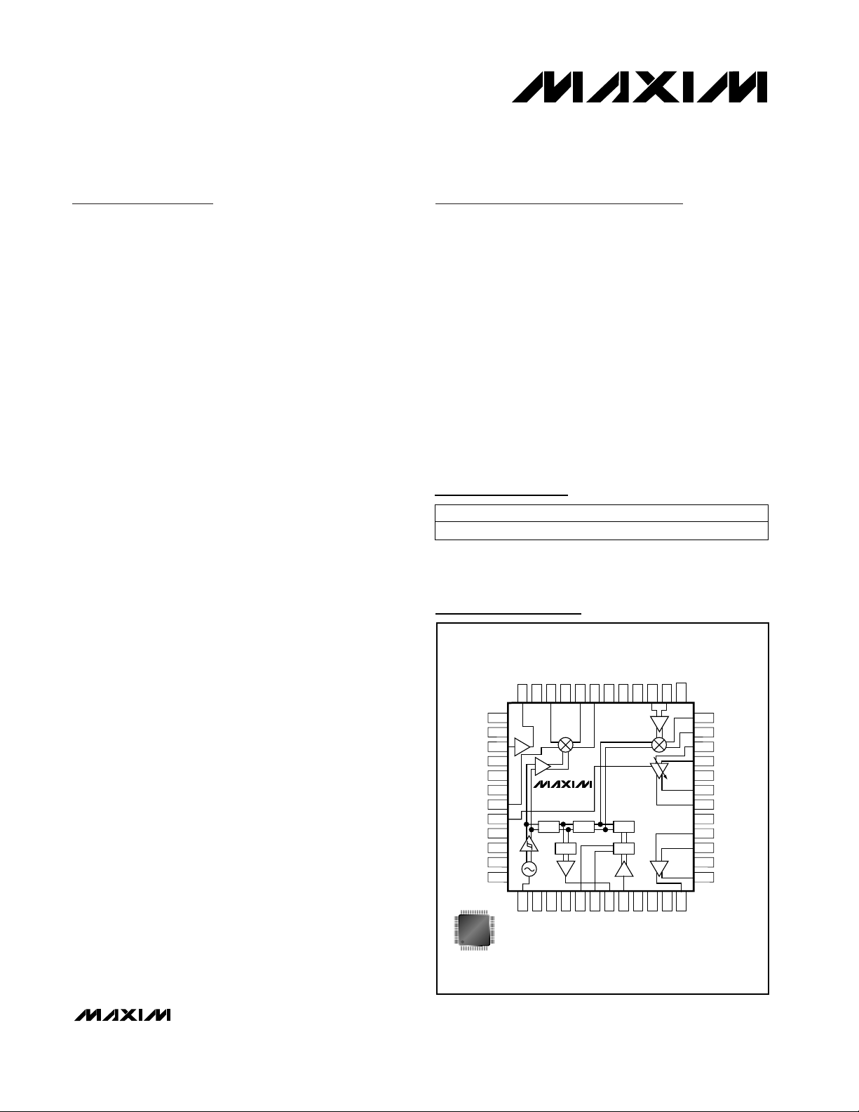
Pin Configuration/
Functional Diagram
19-1670; Rev 0; 4/00
For free samples and the latest literature, visit www.maxim-ic.com or phone 1-800-998-8800.
For small orders, phone 1-800-835-8769.
Ordering Information
48 TQFP-EP*
PIN-PACKAGETEMP. RANGE
-40°C to +85°CMAX2740ECM
PART
*Exposed paddle
LNA_OUT
GND
RFMIX_IN+
VCC_RFMIX
RFMIX_OUT+
RFMIX_OUT-
GND
GND
VCC_IFMIX
IFMIX_IN+
IFMIX_IN-
GND
GND
GND
LNA_IN
GND
GND
GND
RFMIX_IN-
VCC_ANA
GND
GND
VCC_VCO
4847464544434241403938
1
2
3
4
5
6
7
GC
8
9
10
11
12
MAX2740
/2 /6
/8
/6
PFD
37
36
IFMIX_OUT+
35
IFMIX_OUT-
34
VGA_IN+
33
VGA_INGND
32
VGA_OUT+
31
VGA_OUT-
30
GND
29
FGA_IN+
28
FGA_IN-
27
GND
26
FGA_OUT+
25
48
TQFP
ACTUAL SIZE
9mm x 9mm
1314151617181920212223
TANK
GND
GND
UP
DOWN
VCC_DIG
TQFP-EP
REF_IN
GLS_OUT
GND
GND
24
GND
FGA_OUT-
Page 2
MAX2740
Integrated GPS Receiver and Synthesizer
2 _______________________________________________________________________________________
ABSOLUTE MAXIMUM RATINGS
DC ELECTRICAL CHARACTERISTICS
(VCC= +2.7V to +3.3V, TA= -40°C to +85°C. Typical values are at VCC= +3.0, TA= +25°C.)
AC ELECTRICAL CHARACTERISTICS
(MAX2740 EV kit, VCC= +3.0V, 50Ω system impedance, FRF= 1575.42MHz, F
IF1
= 135.42MHz, F
IF2
= 15.42MHz, F
REF
= 20MHz at
600mVpp, T
A
= +25°C, unless otherwise noted.)
Stresses beyond those listed under “Absolute Maximum Ratings” may cause permanent damage to the device. These are stress ratings only, and functional
operation of the device at these or any other conditions beyond those indicated in the operational sections of the specifications is not implied. Exposure to
absolute maximum rating conditions for extended periods may affect device reliability.
VCCPins to GND ...................................................-0.3V to +4.3V
RF LNA Input Power .......................................................+10dBm
LO Input Power...............................................................+10dBm
GC Input Voltage ..........................................-0.3 to (V
CC
+ 0.3V)
Continuous Power Dissipation (T
A
= +85°C)
48-Pin TQFP-EP Package ...........................................800mW
Operating Temperature Range ...........................-40°C to +85°C
Junction Temperature......................................................+150°C
Storage Temperature Range .............................-65°C to +160°C
Lead Temperature (soldering, 10s) .................................+300°C
Total Supply Current 55.1 84.3 mA
AGC Voltage Range
AGC Current -50 +25 µA
PARAMETER CONDITIONS MIN TYP MAX UNITS
0.5 to
2.5
V
LNA
LNA Gain (Note 1) 13.1 16.0 17.2 dB
LNA Gain Variation Over
Temperature
LNA Input Third-Order Intercept
Point
LNA Noise Figure 2.6 dB
RF MIXER (Zl = 100Ω differential)
RF Mixer Conversion Gain (Note 3) 22.6 dB
RF Mixer Input IP3 -22.4 dBm
RF Mixer Noise Figure (SSB) 11.0 dB
IF MIXER (Z
IF Mixer Conversion Gain 36.3 dB
VARIABLE-GAIN AMPLIFIER (VGA) (Z
VGA Voltage Gain at Maximum
Gain Setting
VGA Voltage Gain at Minimum
Gain Setting
FIXED GAIN AMPLIFIER (FGA)
FGA Voltage Gain Z
FGA 1dB Compression (Output)
PARAMETER CONDITIONS MIN TYP MAX UNITS
Relative to ambient (Note 1) -1.3 ±0.5 +1.0 dB
(Note 2) -9.4 dBm
= 100Ω differential, Z
s
= 4kΩ differential)
l
= 4kΩ differential)
l
GC = 2.5V 15.1 dB
GC = 0.5V -54.7 dB
= 4kΩ differential 39.8 dB
l
2.05 Vp-p
Page 3
MAX2740
Integrated GPS Receiver and Synthesizer
_______________________________________________________________________________________ 3
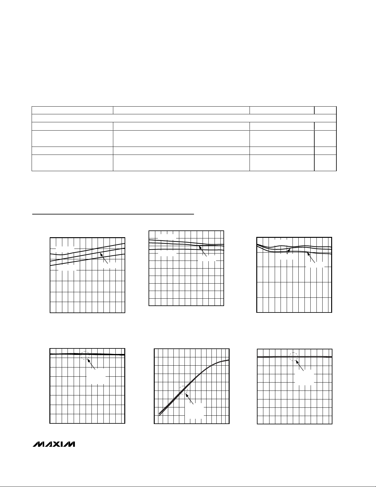
GAIN
(dB)
Typical Operating Characteristics
(TA = +25°C, unless otherwise noted.)
Note 1: Guaranteed by design and characterization.
Note 2: Two tones at pin = -35dBm per tone, f1 = 1575MHz, f2 = 1576MHz.
Note 3: Two tones at pin = -40dBm per tone, f1 = 1575MHz, f2 = 1576MHz.
AC ELECTRICAL CHARACTERISTICS (continued)
(MAX2740 EV kit, VCC= +3.0V, 50Ω system impedance, FRF= 1575.42MHz, F
IF1
= 135.42MHz, F
IF2
= 15.42MHz, F
REF
= 20MHz at
600mVpp, T
A
= +25°C, unless otherwise noted.)
PARAMETER CONDITIONS MIN TYP MAX UNITS
VOLTAGE-CONTROLLED OSCILLATOR (VCO) (100kHz offset)
Synthesizer VCO Phase Noise -91.5 dBc/Hz
Output Frequency for External
GLONASS Tuner
Magnitude GLS_OUT Rl = 500Ω, Cl = 10pF 300 mVp-p
PFD Swing on Up and Down
Outputs
Mag (UP-DOWN) 250 mV
VCC = 3.0V
40 50
20 30
ICC vs. TEMPERATURE AND V
70
60
VCC = 3.3V
50
VCC = 2.7V
40
30
CURRENT (mA)
20
10
0
-40 -30
-20
010
-10 60
TEMPERATURE (°C)
20 30
CC
VCC = 3.0V
40 50
LNA GAIN vs. TEMPERATURE AND V
20
VCC = 3.3V
18
16
MAX2740-01
14
VCC = 2.7V
12
10
8
6
4
2
0
-40 -30
-20
010
-10 60
8070
TEMPERATURE (°C)
CC
MAX2740-02
8070
25
20
15
GAIN (dB)
10
5
0
90 MHz
RF MIXER GAIN
vs. TEMPERATURE AND V
VCC = 3.3V
VCC = 3.0V
-40 -30
-20
010
-10 60
TEMPERATURE (°C)
20 30
VCC = 2.7V
40 50
CC
MAX2740-06
8070
40
35
30
25
20
GAIN (dB)
15
10
5
0
IF MIXER GAIN vs.
TEMPERATURE AND V
-40 -30
-20
-10 60
VGA GAIN vs. VGC AND
CC
= 3.0V
2.2
FGA GAIN vs. TEMPERATURE AND V
45
40
MAX2740-04
35
30
25
20
GAIN (dB)
15
10
5
2.4
0
-40 -30
-20
-10 60
VCC = 2.7V
= 3.3V
V
CC
= 3.0V
V
CC
010
TEMPERATURE (°C)
20 30
40 50
VCC = 2.7V
= 3.3V
V
CC
= 3.0V
V
CC
010
TEMPERATURE (°C)
20 30
40 50
CC
MAX2740-03
VGA GAIN (dB)
8070
TEMPERATURE AT V
30
20
10
0
-10
-20
-30
-40
-50
-60
1.0 1.2 1.4 1.6 1.8 2.0
TA = +25°C
T
A
T
A
AGC CONTROL VOLTAGE (V)
= +85°C
= -40°C
CC
MAX2740-05
8070
Page 4

MAX2740
Integrated GPS Receiver and Synthesizer
4 _______________________________________________________________________________________
Pin Description
PIN NAME FUNCTION
1, 2, 4, 5, 6,
10, 11, 14, 15,
21, 22, 23, 26,
29, 32, 37, 41,
42, 47,
p ad d l e
3 LNA_IN Input of LNA Circuit. Matching network and blocking capacitor required.
7 RFMIX_IN-
8GC
9 VCC_ANA Supply Voltage Pin for Analog Circuits. This pin requires external decoupling of typically 0.01µF.
12 VCC_VCO Supply Voltage Pin for VCO Circuit. This pin requires external decoupling of typically 1000pF.
13 TANK VCO Resonator Pin. A resonator is required at this pin.
16 VCC_DIG
17 DOWN
18 UP
19 GLS_OUT Output of Buffer that Provides a 90MHz Clock Signal. Requires external blocking capacitor.
GND Ground. Connect pin to ground.
Input to unused side of a differential pair that forms the RF section of a Gilbert cell mixer. This pin
should be AC-grounded through 100pF.
DC Control Voltage for Setting Gain Level of VGA. High input impedance. Voltage range of 0.5V
to 2.5V.
Supply Voltage Pin for Digital Section of the IC. This pin requires external decoupling of typically
0.01µF.
Down Output from the Phase-Frequency Detector. This pulses high whenever the phase of the
VCO leads the phase of the reference.
Up Output from the Phase-Frequency Detector. This pulses high whenever the phase of the VCO
lags the phase of the reference.
20 REF_IN Reference Input for Synthesizer
24 FGA_OUT- FGA Inverted Output. Blocking capacitor required.
25 FGA_OUT+ FGA Noninverted Output. Blocking capacitor required.
27 FGA_IN- FGA Inverted Input. Blocking capacitor required.
28 FGA_IN+ FGA Noninverted Input. Blocking capacitor required.
30 VGA_OUT- VGA Inverted Output. Blocking capacitor required.
31 VGA_OUT+ VGA Noninverted Output. Blocking capacitor required.
33 VGA_IN- VGA Inverted Input. Blocking capacitor required.
34 VGA_IN+ VGA Noninverted Input. Blocking capacitor required.
35 IFMIX_OUT- IF Mixer Inverted Output. Blocking capacitor required.
36 IFMIX_OUT+ IF Mixer Noninverted Output. Blocking capacitor required.
38 IFMIX_IN- IF Mixer Inverted Input. Blocking capacitor required.
39 IFMIX_IN+ IF Mixer Noninverted Input. Blocking capacitor required.
40 VCC_IFMIX
Supply Voltage Pin for IF Downconverter. This pin requires external decoupling of typically
1000pF.
Page 5

MAX2740
Integrated GPS Receiver and Synthesizer
_______________________________________________________________________________________ 5
Pin Description (continued)
Figure 1. Typical Application Circuit
PIN NAME FUNCTION
43 RFMIX_OUT- RF Mixer Inverted Input (same as RFMIX_OUT+)
44 RFMIX_OUT+
45 VCC_RFMIX
Open Emitter Output of the RF Downconverter. This pin requires an external pull-down resistor of
1.2kΩ to establish the correct on-chip bias conditions. Requires a blocking capacitor.
Supply Voltage Pin for RF Downconverter. This pin requires external decoupling of typically
100pF.
46 RFMIX_IN Input to RF Mixer. Requires a blocking capacitor that may be used as part of the match network.
48 LNA_OUT
LNA Output. Requires a pull-up inductor and a blocking capacitor. These may be configured as
the matching network.
MAX2740
V
CC
AGC
GAIN SET
MAX4122
4847464544434241403938
1
2
3
4
5
6
7
8
9
10
11
12
/2 /6
/8
1314151617181920212223
/6
PFD
37
36
35
34
33
32
31
30
29
28
27
26
25
TO DSP
24
20MHz
MAX4122
Page 6

MAX2740
Applications Information
Figure 1 shows a typical application diagram in which
the MAX2740 should be used. The RF front end consists of the antenna interface, MAX2740, two control
loops (one for the AGC, the other for the synthesizer),
and appropriate external components, including filters
for image rejection and channel selectivity, operational
amplifiers for the control loops, and resonator and tuning network for the VCO.
Only the antenna input, an external 20MHz frequency
reference, and an AGC input from the accompanying
DSP are required. A differential output is provided from
the MAX2740, which can be applied either to the external analog-to-digital conversion circuitry or directly to
the companion DSP.
Low-Noise Amplifier
This subcircuit requires input and output matching. The
input match is typically a series capacitor, and the output is typically a shunt inductor to VCCand a series
capacitor.
RF Mixer
The RF input is matched externally. The match consists
of a series inductor and shunt capacitor. The source
impedance for this circuit is the single-ended, 50Ω RF
SAW used as an image reject filter. A second RF input
is brought out to a separate pin for AC grounding. This
ensures low ground impedance over a wide band and
minimizes amplification of any noise at the IF frequency
generated within the mixer structure.
The IF output is delivered through low-output-impedance emitter followers and is suitable for directly driving
a 135MHz IF SAW with a typical impedance of 400Ω.
The deliberate mismatch keeps the group delay distortion of the SAW within an acceptable level.
IF Mixer
The IF downconverter receives the differential 1st IF of
135.42MHz from the SAW and delivers a differential
2nd IF signal at 15.42MHz. The circuit has been optimized to deliver a high level of conversion gain with
adequate IIP3 and noise figure. The circuit is terminated on the input with a differential 100Ω to establish the
correct embedding impedance for the IF SAW. The
emitter follower outputs drive directly into a high-impedance, differential, three-pole lowpass discrete lumped
element filter.
Variable-Gain Amplifier
This circuit compensates for receiver gain variation and
unknown antenna cable losses. Under these conditions, the receiver will exhibit minimum implementation
loss. The circuit has a useful gain control range of
greater than 50dB, with a maximum gain level of 16dB.
Fixed-Gain Amplifier
This circuit has been designed to deliver 40dB of differential gain at the 2nd IF frequency of 15.42MHz. The
differential inputs are received from the VGA outputs
through a balanced lowpass filter circuit. The circuit’s
differential output is designed to drive a digitizer with a
typical load impedance of 4kΩ differential.
Voltage-Controlled Oscillator
The core of the L-band VCO is based on a commoncollector Colpitts topology. This circuit has been optimized for low thermal noise and high signal swing without asymmetrical clipping. The circuit is designed for
use with a lumped inductor for low-cost applications.
The self-resonance should be above 1440MHz so that
parallel varactor tuning and the VCO internal capacitance produces resonance at 1440MHz.
Synthesizer
The digital prescaler accepts the output from the oscillator’s differential digital buffer and divides the frequency from 1.44GHz to 120MHz for the 2nd LO, 20MHz for
the phase-frequency detector, and 90MHz for the
GLONASS reference output. Divider blocks are
arranged to ensure that the 2nd LO drive has minimum
duty cycle distortion. A simple output buffer is used to
deliver the GLONASS reference signal to a typical
external load impedance of 500Ω.
The phase-frequency detector is a classical dual flipflop with ANDed feedback to a reset function. UP and
DOWN outputs are provided through emitter follower
buffers. These outputs deliver pulse-width-modulated
signals that in phase-acquisition mode give a phase
detector range of ±2π. With the PLL not in lock, either
the UP or DOWN output will be active and drive the
VCO frequency toward the reference frequency. The
phase detector outputs feed directly into an active,
lead-lag differential loop filter.
Integrated GPS Receiver and Synthesizer
6 _______________________________________________________________________________________
Page 7

MAX2740
Integrated GPS Receiver and Synthesizer
_______________________________________________________________________________________ 7
Package Information
48L,TQFP.EPS
Page 8

MAX2740
Integrated GPS Receiver and Synthesizer
Maxim cannot assume responsibility for use of any circuitry other than circuitry entirely embodied in a Maxim product. No circuit patent licenses are
implied. Maxim reserves the right to change the circuitry and specifications without notice at any time.
8 _____________________Maxim Integrated Products, 120 San Gabriel Drive, Sunnyvale, CA 94086 408-737-7600
© 2000 Maxim Integrated Products Printed USA is a registered trademark of Maxim Integrated Products.
NOTES
 Loading...